
Semiconductor device
Encyclopedia
Semiconductor devices are electronic component
s that exploit the electronic
properties of semiconductor
materials, principally silicon
, germanium
, and gallium arsenide, as well as organic semiconductors. Semiconductor devices have replaced thermionic devices
(vacuum tubes) in most applications. They use electron
ic conduction in the solid state
as opposed to the gaseous state or thermionic emission
in a high vacuum.
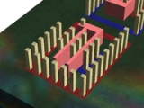
Semiconductor devices are manufactured both as single discrete devices and as integrated circuit
s (ICs), which consist of a number—from a few (as low as two) to billions—of devices manufactured and interconnected on a single semiconductor substrate.
The main reason semiconductor materials are so useful is that the behavior of a semiconductor can be easily manipulated by the addition of impurities, known as doping. Semiconductor conductivity can be controlled by introduction of an electric or magnetic field, by exposure to light
or heat, or by mechanical deformation of a doped monocrystalline
grid; thus, semiconductors can make excellent sensors. Current conduction in a semiconductor
occurs via mobile or "free" electrons and holes
, collectively known as charge carrier
s. Doping a semiconductor such as silicon
with a small amount of impurity atoms, such as phosphorus
or boron
, greatly increases the number of free electrons or holes within the semiconductor. When a doped semiconductor contains excess holes it is called "p-type
", and when it contains excess free electrons it is known as "n-type
", where p (positive for holes
) or n (negative for electron
s) is the sign of the charge of the majority mobile charge carriers. The semiconductor material used in devices is doped under highly controlled conditions in a fabrication facility, or fab, to precisely control the location and concentration of p- and n-type dopants. The junctions which form where n-type and p-type semiconductors join together are called p-n junction
s.
is a device made from a single p-n junction. At the junction of a p-type and an n-type semiconductor there forms a region called the depletion zone which blocks current conduction from the n-type region to the p-type region, but allows current to conduct from the p-type region to the n-type region. Thus when the device is forward biased, with the p-side at higher electric potential
, the diode conducts current easily; but the current is very small when the diode is reverse biased.
Exposing a semiconductor to light
can generate electron–hole pairs, which increases the number of free carriers and its conductivity. Diodes optimized to take advantage of this phenomenon are known as photodiode
s.
Compound semiconductor
diodes can also be used to generate light, as in light-emitting diode
s and laser diode
s.
Another type of transistor, the field effect transistor operates on the principle that semiconductor conductivity can be increased or decreased by the presence of an electric field. An electric field
can increase the number of free electrons and holes in a semiconductor, thereby changing its conductivity. The field may be applied by a reverse-biased p-n junction, forming a junction field effect transistor, or JFET
; or by an electrode isolated from the bulk material by an oxide layer, forming a metal-oxide-semiconductor field effect transistor, or MOSFET
.
The MOSFET is the most used semiconductor device today. The gate electrode is charged to produce an electric field
that controls the conductivity of a "channel" between two terminals, called the source and drain. Depending on the type of carrier in the channel, the device may be an n-channel (for electrons) or a p-channel (for holes) MOSFET. Although the MOSFET is named in part for its "metal" gate, in modern devices polysilicon is typically used instead. MOSFET is an IC which is semiconductor device.
(Si) is the most widely used material in semiconductor devices. Its combination of low raw material cost, relatively simple processing, and a useful temperature range make it currently the best compromise among the various competing materials. Silicon used in semiconductor device manufacturing is currently fabricated into boules
that are large enough in diameter to allow the production of 300 mm (12 in.) wafers.
Germanium
(Ge) was a widely used early semiconductor material but its thermal sensitivity makes it less useful than silicon. Today, germanium is often alloyed with silicon for use in very-high-speed SiGe devices; IBM
is a major producer of such devices.
Gallium arsenide (GaAs) is also widely used in high-speed devices but so far, it has been difficult to form large-diameter boules of this material, limiting the wafer diameter to sizes significantly smaller than silicon wafers thus making mass production of GaAs devices significantly more expensive than silicon.
Other less common materials are also in use or under investigation.
Silicon carbide
(SiC) has found some application as the raw material for blue light-emitting diode
s (LEDs) and is being investigated for use in semiconductor devices that could withstand very high operating temperature
s and environments with the presence of significant levels of ionizing radiation
. IMPATT diode
s have also been fabricated from SiC.
Various indium
compounds (indium arsenide, indium antimonide
, and indium phosphide
) are also being used in LEDs and solid state laser diode
s. Selenium
sulfide
is being studied in the manufacture of photovoltaic solar cell
s.
The most common use for organic semiconductors is Organic light-emitting diode
s.
Three-terminal devices:
Four-terminal devices:
Multi-terminal devices:
s, which are fundamental in the design of digital circuit
s. In digital circuits like microprocessor
s, transistors act as on-off switches; in the MOSFET
, for instance, the voltage
applied to the gate determines whether the switch
is on or off.
Transistors used for analog circuits do not act as on-off switches; rather, they respond to a continuous range of inputs with a continuous range of outputs. Common analog circuits include amplifier
s and oscillators.
Circuits that interface or translate between digital circuits and analog circuits are known as mixed-signal circuit
s.
Power semiconductor device
s are discrete devices or integrated circuits intended for high current or high voltage applications. Power integrated circuits combine IC technology with power semiconductor technology, these are sometimes referred to as "smart" power devices. Several companies specialize in manufacturing power semiconductors.
s, for example, there are three standards: JEDEC
JESD370B in USA
, Pro Electron
in Europe
and JIS in Japan
.
s, used in a device called a "cat's whisker". These detectors were somewhat troublesome, however, requiring the operator to move a small tungsten filament (the whisker) around the surface of a galena
(lead sulfide) or carborundum
(silicon carbide) crystal until it suddenly started working. Then, over a period of a few hours or days, the cat's whisker would slowly stop working and the process would have to be repeated. At the time their operation was completely mysterious. After the introduction of the more reliable and amplified vacuum tube
based radios, the cat's whisker systems quickly disappeared. The "cat's whisker" is a primitive example of a special type of diode still popular today, called a Schottky diode
.
or selenium
. Westinghouse Electric (1886)
was a major manufacturer of these rectifiers.
research quickly pushed radar receivers to operate at ever higher frequencies and the traditional tube based radio receivers no longer worked well. The introduction of the cavity magnetron
from Britain to the United States in 1940 during the Tizard Mission
resulted in a pressing need for a practical high-frequency amplifier.
On a whim, Russell Ohl
of Bell Laboratories decided to try a cat's whisker. By this point they had not been in use for a number of years, and no one at the labs had one. After hunting one down at a used radio store in Manhattan, he found that it worked much better than tube-based systems.
Ohl investigated why the cat's whisker functioned so well. He spent most of 1939 trying to grow more pure versions of the crystals. He soon found that with higher quality crystals their finicky behaviour went away, but so did their ability to operate as a radio detector. One day he found one of his purest crystals nevertheless worked well, and interestingly, it had a clearly visible crack near the middle. However as he moved about the room trying to test it, the detector would mysteriously work, and then stop again. After some study he found that the behaviour was controlled by the light in the room–more light caused more conductance in the crystal. He invited several other people to see this crystal, and Walter Brattain immediately realized there was some sort of junction at the crack.
Further research cleared up the remaining mystery. The crystal had cracked because either side contained very slightly different amounts of the impurities Ohl could not remove–about 0.2%. One side of the crystal had impurities that added extra electrons (the carriers of electrical current) and made it a "conductor". The other had impurities that wanted to bind to these electrons, making it (what he called) an "insulator". Because the two parts of the crystal were in contact with each other, the electrons could be pushed out of the conductive side which had extra electrons (soon to be known as the emitter) and replaced by new ones being provided (from a battery, for instance) where they would flow into the insulating portion and be collected by the whisker filament (named the collector). However, when the voltage was reversed the electrons being pushed into the collector would quickly fill up the "holes" (the electron-needy impurities), and conduction would stop almost instantly. This junction of the two crystals (or parts of one crystal) created a solid-state diode, and the concept soon became known as semiconduction. The mechanism of action when the diode is off has to do with the separation of charge carriers around the junction. This is called a "depletion region
".
, Bell Labs
, MIT
, and the University of Chicago
all joined forces to build better crystals. Within a year germanium production had been perfected to the point where military-grade diodes were being used in most radar sets.
decided to attempt the building of a triode
-like semiconductor device. He secured funding and lab space, and went to work on the problem with Brattain and John Bardeen
.
The key to the development of the transistor was the further understanding of the process of the electron mobility
in a semiconductor. It was realized that if there was some way to control the flow of the electrons from the emitter to the collector of this newly discovered diode, an amplifier could be built. For instance, if contacts are placed on both sides of a single type of crystal, current will not flow between them through the crystal. However if a third contact could then "inject" electrons or holes into the material, current would flow.
Actually doing this appeared to be very difficult. If the crystal were of any reasonable size, the number of electrons (or holes) required to be injected would have to be very large, making it less than useful as an amplifier
because it would require a large injection current to start with. That said, the whole idea of the crystal diode was that the crystal itself could provide the electrons over a very small distance, the depletion region. The key appeared to be to place the input and output contacts very close together on the surface of the crystal on either side of this region.
Brattain started working on building such a device, and tantalizing hints of amplification continued to appear as the team worked on the problem. Sometimes the system would work but then stop working unexpectedly. In one instance a non-working system started working when placed in water. Ohl and Brattain eventually developed a new branch of quantum mechanics
, which became known as surface physics, to account for the behaviour. The electrons in any one piece of the crystal would migrate about due to nearby charges. Electrons in the emitters, or the "holes" in the collectors, would cluster at the surface of the crystal where they could find their opposite charge "floating around" in the air (or water). Yet they could be pushed away from the surface with the application of a small amount of charge from any other location on the crystal. Instead of needing a large supply of injected electrons, a very small number in the right place on the crystal would accomplish the same thing.
Their understanding solved the problem of needing a very small control area to some degree. Instead of needing two separate semiconductors connected by a common, but tiny, region, a single larger surface would serve. The electron-emitting and collecting leads would both be placed very close together on the top, with the control lead placed on the base of the crystal. When current flowed through this "base" lead, the electrons or holes would be pushed out, across the block of semiconductor, and collect on the far surface. As long as the emitter and collector were very close together, this should allow enough electrons or holes between them to allow conduction to start.
 The Bell team made many attempts to build such a system with various tools, but generally failed. Setups where the contacts were close enough were invariably as fragile as the original cat's whisker detectors had been, and would work briefly, if at all. Eventually they had a practical breakthrough. A piece of gold foil was glued to the edge of a plastic wedge, and then the foil was sliced with a razor at the tip of the triangle. The result was two very closely spaced contacts of gold. When the wedge was pushed down onto the surface of a crystal and voltage applied to the other side (on the base of the crystal), current started to flow from one contact to the other as the base voltage pushed the electrons away from the base towards the other side near the contacts. The point-contact transistor had been invented.
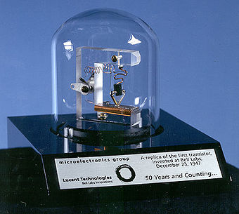
While the device was constructed a week earlier, Brattain's notes describe the first demonstration to higher-ups at Bell Labs on the afternoon of 23 December 1947, often given as the birthdate of the transistor. what is now known as the "PNP point-contact germanium transistor
" operated as a speech amplifier with a power gain of 18 in that trial. John Bardeen
, Walter Houser Brattain
, and William Bradford Shockley were awarded the 1956 Nobel Prize
in physics for their work.
that they thought it best that his name be left off the patent application.
Shockley was incensed, and decided to demonstrate who was the real brains of the operation. A few months later he invented an entirely new, considerably more robust, type of transistor with a layer or 'sandwich' structure. This structure went on to be used for the vast majority of all transistors into the 1960s, and evolved into the bipolar junction transistor
.
With the fragility problems solved, a remaining problem was purity. Making germanium
of the required purity was proving to be a serious problem, and limited the yield of transistors that actually worked from a given batch of material. Germanium's sensitivity to temperature also limited its usefulness. Scientists theorized that silicon would be easier to fabricate, but few investigated this possibility. Gordon K. Teal
was the first to develop a working silicon transistor, and his company, the nascent Texas Instruments
, profited from its technological edge. From the late 1960s most transistors were silicon-based. Within a few years transistor-based products, most notably easily portable radios, were appearing on the market.
A major improvement in manufacturing yield came when a chemist advised the companies fabricating semiconductors to use distilled
rather than tap water: calcium
ion
s present in tap water were the cause of the poor yields. "Zone melting
", a technique using a band of molten material moving through the crystal, further increased crystal purity.
:Category:Semiconductor device fabrication
Electronic component
An electronic component is a basic electronic element and may be available in a discrete form having two or more electrical terminals . These are intended to be connected together, usually by soldering to a printed circuit board, in order to create an electronic circuit with a particular function...
s that exploit the electronic
Electronics
Electronics is the branch of science, engineering and technology that deals with electrical circuits involving active electrical components such as vacuum tubes, transistors, diodes and integrated circuits, and associated passive interconnection technologies...
properties of semiconductor
Semiconductor
A semiconductor is a material with electrical conductivity due to electron flow intermediate in magnitude between that of a conductor and an insulator. This means a conductivity roughly in the range of 103 to 10−8 siemens per centimeter...
materials, principally silicon
Silicon
Silicon is a chemical element with the symbol Si and atomic number 14. A tetravalent metalloid, it is less reactive than its chemical analog carbon, the nonmetal directly above it in the periodic table, but more reactive than germanium, the metalloid directly below it in the table...
, germanium
Germanium
Germanium is a chemical element with the symbol Ge and atomic number 32. It is a lustrous, hard, grayish-white metalloid in the carbon group, chemically similar to its group neighbors tin and silicon. The isolated element is a semiconductor, with an appearance most similar to elemental silicon....
, and gallium arsenide, as well as organic semiconductors. Semiconductor devices have replaced thermionic devices
Vacuum tube
In electronics, a vacuum tube, electron tube , or thermionic valve , reduced to simply "tube" or "valve" in everyday parlance, is a device that relies on the flow of electric current through a vacuum...
(vacuum tubes) in most applications. They use electron
Electron
The electron is a subatomic particle with a negative elementary electric charge. It has no known components or substructure; in other words, it is generally thought to be an elementary particle. An electron has a mass that is approximately 1/1836 that of the proton...
ic conduction in the solid state
Solid state (electronics)
Solid-state electronics are those circuits or devices built entirely from solid materials and in which the electrons, or other charge carriers, are confined entirely within the solid material...
as opposed to the gaseous state or thermionic emission
Thermionic emission
Thermionic emission is the heat-induced flow of charge carriers from a surface or over a potential-energy barrier. This occurs because the thermal energy given to the carrier overcomes the binding potential, also known as work function of the metal. The charge carriers can be electrons or ions, and...
in a high vacuum.
Semiconductor devices are manufactured both as single discrete devices and as integrated circuit
Integrated circuit
An integrated circuit or monolithic integrated circuit is an electronic circuit manufactured by the patterned diffusion of trace elements into the surface of a thin substrate of semiconductor material...
s (ICs), which consist of a number—from a few (as low as two) to billions—of devices manufactured and interconnected on a single semiconductor substrate.
The main reason semiconductor materials are so useful is that the behavior of a semiconductor can be easily manipulated by the addition of impurities, known as doping. Semiconductor conductivity can be controlled by introduction of an electric or magnetic field, by exposure to light
Light
Light or visible light is electromagnetic radiation that is visible to the human eye, and is responsible for the sense of sight. Visible light has wavelength in a range from about 380 nanometres to about 740 nm, with a frequency range of about 405 THz to 790 THz...
or heat, or by mechanical deformation of a doped monocrystalline
Monocrystalline silicon
Monocrystalline silicon or single-crystal Si, or mono-Si is the base material of the electronic industry. It consists of silicon in which the crystal lattice of the entire solid is continuous, unbroken to its edges. It can be prepared intrinsic, i.e...
grid; thus, semiconductors can make excellent sensors. Current conduction in a semiconductor
Semiconductor
A semiconductor is a material with electrical conductivity due to electron flow intermediate in magnitude between that of a conductor and an insulator. This means a conductivity roughly in the range of 103 to 10−8 siemens per centimeter...
occurs via mobile or "free" electrons and holes
Electron hole
An electron hole is the conceptual and mathematical opposite of an electron, useful in the study of physics, chemistry, and electrical engineering. The concept describes the lack of an electron at a position where one could exist in an atom or atomic lattice...
, collectively known as charge carrier
Charge carrier
In physics, a charge carrier is a free particle carrying an electric charge, especially the particles that carry electric currents in electrical conductors. Examples are electrons and ions...
s. Doping a semiconductor such as silicon
Silicon
Silicon is a chemical element with the symbol Si and atomic number 14. A tetravalent metalloid, it is less reactive than its chemical analog carbon, the nonmetal directly above it in the periodic table, but more reactive than germanium, the metalloid directly below it in the table...
with a small amount of impurity atoms, such as phosphorus
Phosphorus
Phosphorus is the chemical element that has the symbol P and atomic number 15. A multivalent nonmetal of the nitrogen group, phosphorus as a mineral is almost always present in its maximally oxidized state, as inorganic phosphate rocks...
or boron
Boron
Boron is the chemical element with atomic number 5 and the chemical symbol B. Boron is a metalloid. Because boron is not produced by stellar nucleosynthesis, it is a low-abundance element in both the solar system and the Earth's crust. However, boron is concentrated on Earth by the...
, greatly increases the number of free electrons or holes within the semiconductor. When a doped semiconductor contains excess holes it is called "p-type
P-type semiconductor
A P-type semiconductor is obtained by carrying out a process of doping: that is, adding a certain type of atoms to the semiconductor in order to increase the number of free charge carriers ....
", and when it contains excess free electrons it is known as "n-type
N-type semiconductor
N-type semiconductors are a type of extrinsic semiconductor where the dopant atoms are capable of providing extra conduction electrons to the host material . This creates an excess of negative electron charge carriers....
", where p (positive for holes
Electron hole
An electron hole is the conceptual and mathematical opposite of an electron, useful in the study of physics, chemistry, and electrical engineering. The concept describes the lack of an electron at a position where one could exist in an atom or atomic lattice...
) or n (negative for electron
Electron
The electron is a subatomic particle with a negative elementary electric charge. It has no known components or substructure; in other words, it is generally thought to be an elementary particle. An electron has a mass that is approximately 1/1836 that of the proton...
s) is the sign of the charge of the majority mobile charge carriers. The semiconductor material used in devices is doped under highly controlled conditions in a fabrication facility, or fab, to precisely control the location and concentration of p- and n-type dopants. The junctions which form where n-type and p-type semiconductors join together are called p-n junction
P-n junction
A p–n junction is formed at the boundary between a P-type and N-type semiconductor created in a single crystal of semiconductor by doping, for example by ion implantation, diffusion of dopants, or by epitaxy .If two separate pieces of material were used, this would...
s.
Diode
The diodeDiode
In electronics, a diode is a type of two-terminal electronic component with a nonlinear current–voltage characteristic. A semiconductor diode, the most common type today, is a crystalline piece of semiconductor material connected to two electrical terminals...
is a device made from a single p-n junction. At the junction of a p-type and an n-type semiconductor there forms a region called the depletion zone which blocks current conduction from the n-type region to the p-type region, but allows current to conduct from the p-type region to the n-type region. Thus when the device is forward biased, with the p-side at higher electric potential
Electric potential
In classical electromagnetism, the electric potential at a point within a defined space is equal to the electric potential energy at that location divided by the charge there...
, the diode conducts current easily; but the current is very small when the diode is reverse biased.
Exposing a semiconductor to light
Light
Light or visible light is electromagnetic radiation that is visible to the human eye, and is responsible for the sense of sight. Visible light has wavelength in a range from about 380 nanometres to about 740 nm, with a frequency range of about 405 THz to 790 THz...
can generate electron–hole pairs, which increases the number of free carriers and its conductivity. Diodes optimized to take advantage of this phenomenon are known as photodiode
Photodiode
A photodiode is a type of photodetector capable of converting light into either current or voltage, depending upon the mode of operation.The common, traditional solar cell used to generateelectric solar power is a large area photodiode....
s.
Compound semiconductor
Compound semiconductor
A compound semiconductor is a semiconductor compound composed of elements from two or more different groups of the periodic table . These semiconductors typically form in groups 13-16 ,...
diodes can also be used to generate light, as in light-emitting diode
Light-emitting diode
A light-emitting diode is a semiconductor light source. LEDs are used as indicator lamps in many devices and are increasingly used for other lighting...
s and laser diode
Laser diode
The laser diode is a laser where the active medium is a semiconductor similar to that found in a light-emitting diode. The most common type of laser diode is formed from a p-n junction and powered by injected electric current...
s.
Transistor
Bipolar junction transistors are formed from two p-n junctions, in either n-p-n or p-n-p configuration. The middle, or base, region between the junctions is typically very narrow. The other regions, and their associated terminals, are known as the emitter and the collector. A small current injected through the junction between the base and the emitter changes the properties of the base-collector junction so that it can conduct current even though it is reverse biased. This creates a much larger current between the collector and emitter, controlled by the base-emitter current.Another type of transistor, the field effect transistor operates on the principle that semiconductor conductivity can be increased or decreased by the presence of an electric field. An electric field
Electric field
In physics, an electric field surrounds electrically charged particles and time-varying magnetic fields. The electric field depicts the force exerted on other electrically charged objects by the electrically charged particle the field is surrounding...
can increase the number of free electrons and holes in a semiconductor, thereby changing its conductivity. The field may be applied by a reverse-biased p-n junction, forming a junction field effect transistor, or JFET
JFET
The junction gate field-effect transistor is the simplest type of field-effect transistor. It can be used as an electronically-controlled switch or as a voltage-controlled resistance. Electric charge flows through a semiconducting channel between "source" and "drain" terminals...
; or by an electrode isolated from the bulk material by an oxide layer, forming a metal-oxide-semiconductor field effect transistor, or MOSFET
MOSFET
The metal–oxide–semiconductor field-effect transistor is a transistor used for amplifying or switching electronic signals. The basic principle of this kind of transistor was first patented by Julius Edgar Lilienfeld in 1925...
.
The MOSFET is the most used semiconductor device today. The gate electrode is charged to produce an electric field
Electric field
In physics, an electric field surrounds electrically charged particles and time-varying magnetic fields. The electric field depicts the force exerted on other electrically charged objects by the electrically charged particle the field is surrounding...
that controls the conductivity of a "channel" between two terminals, called the source and drain. Depending on the type of carrier in the channel, the device may be an n-channel (for electrons) or a p-channel (for holes) MOSFET. Although the MOSFET is named in part for its "metal" gate, in modern devices polysilicon is typically used instead. MOSFET is an IC which is semiconductor device.
Semiconductor device materials
By far, siliconSilicon
Silicon is a chemical element with the symbol Si and atomic number 14. A tetravalent metalloid, it is less reactive than its chemical analog carbon, the nonmetal directly above it in the periodic table, but more reactive than germanium, the metalloid directly below it in the table...
(Si) is the most widely used material in semiconductor devices. Its combination of low raw material cost, relatively simple processing, and a useful temperature range make it currently the best compromise among the various competing materials. Silicon used in semiconductor device manufacturing is currently fabricated into boules
Boule (crystal)
A boule is a single-crystal ingot produced by synthetic means. A boule of silicon is the starting material for most of the integrated circuits used today....
that are large enough in diameter to allow the production of 300 mm (12 in.) wafers.
Germanium
Germanium
Germanium is a chemical element with the symbol Ge and atomic number 32. It is a lustrous, hard, grayish-white metalloid in the carbon group, chemically similar to its group neighbors tin and silicon. The isolated element is a semiconductor, with an appearance most similar to elemental silicon....
(Ge) was a widely used early semiconductor material but its thermal sensitivity makes it less useful than silicon. Today, germanium is often alloyed with silicon for use in very-high-speed SiGe devices; IBM
IBM
International Business Machines Corporation or IBM is an American multinational technology and consulting corporation headquartered in Armonk, New York, United States. IBM manufactures and sells computer hardware and software, and it offers infrastructure, hosting and consulting services in areas...
is a major producer of such devices.
Gallium arsenide (GaAs) is also widely used in high-speed devices but so far, it has been difficult to form large-diameter boules of this material, limiting the wafer diameter to sizes significantly smaller than silicon wafers thus making mass production of GaAs devices significantly more expensive than silicon.
Other less common materials are also in use or under investigation.
Silicon carbide
Silicon carbide
Silicon carbide , also known as carborundum, is a compound of silicon and carbon with chemical formula SiC. It occurs in nature as the extremely rare mineral moissanite. Silicon carbide powder has been mass-produced since 1893 for use as an abrasive...
(SiC) has found some application as the raw material for blue light-emitting diode
Light-emitting diode
A light-emitting diode is a semiconductor light source. LEDs are used as indicator lamps in many devices and are increasingly used for other lighting...
s (LEDs) and is being investigated for use in semiconductor devices that could withstand very high operating temperature
Operating temperature
An operating temperature is the temperature at which an electrical or mechanical device operates. The device will operate effectively within a specified temperature range which varies based on the device function and application context, and ranges from the minimum operating temperature to the...
s and environments with the presence of significant levels of ionizing radiation
Ionizing radiation
Ionizing radiation is radiation composed of particles that individually have sufficient energy to remove an electron from an atom or molecule. This ionization produces free radicals, which are atoms or molecules containing unpaired electrons...
. IMPATT diode
IMPATT diode
An IMPATT diode is a form of high power diode used in high-frequency electronics and microwave devices. They are typically made with silicon carbide owing to their high breakdown fields....
s have also been fabricated from SiC.
Various indium
Indium
Indium is a chemical element with the symbol In and atomic number 49. This rare, very soft, malleable and easily fusible post-transition metal is chemically similar to gallium and thallium, and shows the intermediate properties between these two...
compounds (indium arsenide, indium antimonide
Antimony
Antimony is a toxic chemical element with the symbol Sb and an atomic number of 51. A lustrous grey metalloid, it is found in nature mainly as the sulfide mineral stibnite...
, and indium phosphide
Phosphorus
Phosphorus is the chemical element that has the symbol P and atomic number 15. A multivalent nonmetal of the nitrogen group, phosphorus as a mineral is almost always present in its maximally oxidized state, as inorganic phosphate rocks...
) are also being used in LEDs and solid state laser diode
Laser diode
The laser diode is a laser where the active medium is a semiconductor similar to that found in a light-emitting diode. The most common type of laser diode is formed from a p-n junction and powered by injected electric current...
s. Selenium
Selenium
Selenium is a chemical element with atomic number 34, chemical symbol Se, and an atomic mass of 78.96. It is a nonmetal, whose properties are intermediate between those of adjacent chalcogen elements sulfur and tellurium...
sulfide
Sulfide
A sulfide is an anion of sulfur in its lowest oxidation state of 2-. Sulfide is also a slightly archaic term for thioethers, a common type of organosulfur compound that are well known for their bad odors.- Properties :...
is being studied in the manufacture of photovoltaic solar cell
Solar cell
A solar cell is a solid state electrical device that converts the energy of light directly into electricity by the photovoltaic effect....
s.
The most common use for organic semiconductors is Organic light-emitting diode
Organic light-emitting diode
An OLED is a light-emitting diode in which the emissive electroluminescent layer is a film of organic compounds which emit light in response to an electric current. This layer of organic semiconductor material is situated between two electrodes...
s.
List of common semiconductor devices
Two-terminal devices:- DIACDIACThe DIAC, or 'diode for alternating current', is a diode that conducts current only after its breakover voltage has been reached momentarily....
- DiodeDiodeIn electronics, a diode is a type of two-terminal electronic component with a nonlinear current–voltage characteristic. A semiconductor diode, the most common type today, is a crystalline piece of semiconductor material connected to two electrical terminals...
(rectifier diode) - Gunn diodeGunn diodeA Gunn diode, also known as a transferred electron device , is a form of diode used in high-frequency electronics. It is somewhat unusual in that it consists only of N-doped semiconductor material, whereas most diodes consist of both P and N-doped regions...
- IMPATT diodeIMPATT diodeAn IMPATT diode is a form of high power diode used in high-frequency electronics and microwave devices. They are typically made with silicon carbide owing to their high breakdown fields....
- Laser diodeLaser diodeThe laser diode is a laser where the active medium is a semiconductor similar to that found in a light-emitting diode. The most common type of laser diode is formed from a p-n junction and powered by injected electric current...
- Light-emitting diodeLight-emitting diodeA light-emitting diode is a semiconductor light source. LEDs are used as indicator lamps in many devices and are increasingly used for other lighting...
(LED) - Photocell
- PIN diodePIN diodeA PIN diode is a diode with a wide, lightly doped 'near' intrinsic semiconductor region between a p-type semiconductor and an n-type semiconductor region. The p-type and n-type regions are typically heavily doped because they are used for ohmic contacts....
- Schottky diodeSchottky diodeThe Schottky diode is a semiconductor diode with a low forward voltage drop and a very fast switching action...
- Solar cellSolar cellA solar cell is a solid state electrical device that converts the energy of light directly into electricity by the photovoltaic effect....
- Tunnel diodeTunnel diodeA tunnel diode or Esaki diode is a type of semiconductor diode which is capable of very fast operation, well into the microwave frequency region, by using quantum mechanical effects....
- VCSELVCSELThe vertical-cavity surface-emitting laser, or VCSEL , is a type of semiconductor laser diode with laser beam emission perpendicular from the top surface, contrary to conventional edge-emitting semiconductor lasers which emit from surfaces formed by cleaving the individual chip out of a...
- VECSELVECSELA vertical-external-cavity surface-emitting-laser is a small semiconductor laser similar to a vertical-cavity surface-emitting laser...
- Zener diodeZener diodeA Zener diode is a special kind of diode which allows current to flow in the forward direction in the same manner as an ideal diode, but will also permit it to flow in the reverse direction when the voltage is above a certain value known as the breakdown voltage, "Zener knee voltage" or "Zener...
Three-terminal devices:
- Bipolar transistor
- Darlington transistorDarlington transistorIn electronics, the Darlington transistor is a compound structure consisting of two bipolar transistors connected in such a way that the current amplified by the first transistor is amplified further by the second one...
- Field-effect transistorField-effect transistorThe field-effect transistor is a transistor that relies on an electric field to control the shape and hence the conductivity of a channel of one type of charge carrier in a semiconductor material. FETs are sometimes called unipolar transistors to contrast their single-carrier-type operation with...
, including MOSFETMOSFETThe metal–oxide–semiconductor field-effect transistor is a transistor used for amplifying or switching electronic signals. The basic principle of this kind of transistor was first patented by Julius Edgar Lilienfeld in 1925... - IGBT transistor
- Silicon controlled rectifier
- ThyristorThyristorA thyristor is a solid-state semiconductor device with four layers of alternating N and P-type material. They act as bistable switches, conducting when their gate receives a current trigger, and continue to conduct while they are forward biased .Some sources define silicon controlled rectifiers and...
- TRIACTRIACTRIAC, from Triode for Alternating Current, is a genericized tradename for an electronic component that can conduct current in either direction when it is triggered , and is formally called a bidirectional triode thyristor or bilateral triode thyristor.TRIACs belong to the thyristor family and are...
- Unijunction transistorUnijunction transistorA unijunction transistor is an electronic semiconductor device that has only one junction. The UJT has three terminals: an emitter and two bases . The base is formed by lightly doped n-type bar of silicon. Two ohmic contacts B1 and B2 are attached at its ends. The emitter is of p-type and it is...
Four-terminal devices:
- Hall effect sensorHall effect sensorA Hall effect sensor is a transducer that varies its output voltage in response to a magnetic field. Hall effect sensors are used for proximity switching, positioning, speed detection, and current sensing applications....
(magnetic field sensor)
Multi-terminal devices:
- Integrated circuitIntegrated circuitAn integrated circuit or monolithic integrated circuit is an electronic circuit manufactured by the patterned diffusion of trace elements into the surface of a thin substrate of semiconductor material...
(ICs) - Charge-coupled deviceCharge-coupled deviceA charge-coupled device is a device for the movement of electrical charge, usually from within the device to an area where the charge can be manipulated, for example conversion into a digital value. This is achieved by "shifting" the signals between stages within the device one at a time...
(CCD) - MicroprocessorMicroprocessorA microprocessor incorporates the functions of a computer's central processing unit on a single integrated circuit, or at most a few integrated circuits. It is a multipurpose, programmable device that accepts digital data as input, processes it according to instructions stored in its memory, and...
- Random-access memoryRandom-access memoryRandom access memory is a form of computer data storage. Today, it takes the form of integrated circuits that allow stored data to be accessed in any order with a worst case performance of constant time. Strictly speaking, modern types of DRAM are therefore not random access, as data is read in...
(RAM) - Read-only memoryRead-only memoryRead-only memory is a class of storage medium used in computers and other electronic devices. Data stored in ROM cannot be modified, or can be modified only slowly or with difficulty, so it is mainly used to distribute firmware .In its strictest sense, ROM refers only...
(ROM)
Semiconductor device applications
All transistor types can be used as the building blocks of logic gateLogic gate
A logic gate is an idealized or physical device implementing a Boolean function, that is, it performs a logical operation on one or more logic inputs and produces a single logic output. Depending on the context, the term may refer to an ideal logic gate, one that has for instance zero rise time and...
s, which are fundamental in the design of digital circuit
Digital circuit
Digital electronics represent signals by discrete bands of analog levels, rather than by a continuous range. All levels within a band represent the same signal state...
s. In digital circuits like microprocessor
Microprocessor
A microprocessor incorporates the functions of a computer's central processing unit on a single integrated circuit, or at most a few integrated circuits. It is a multipurpose, programmable device that accepts digital data as input, processes it according to instructions stored in its memory, and...
s, transistors act as on-off switches; in the MOSFET
MOSFET
The metal–oxide–semiconductor field-effect transistor is a transistor used for amplifying or switching electronic signals. The basic principle of this kind of transistor was first patented by Julius Edgar Lilienfeld in 1925...
, for instance, the voltage
Voltage
Voltage, otherwise known as electrical potential difference or electric tension is the difference in electric potential between two points — or the difference in electric potential energy per unit charge between two points...
applied to the gate determines whether the switch
Switch
In electronics, a switch is an electrical component that can break an electrical circuit, interrupting the current or diverting it from one conductor to another....
is on or off.
Transistors used for analog circuits do not act as on-off switches; rather, they respond to a continuous range of inputs with a continuous range of outputs. Common analog circuits include amplifier
Amplifier
Generally, an amplifier or simply amp, is a device for increasing the power of a signal.In popular use, the term usually describes an electronic amplifier, in which the input "signal" is usually a voltage or a current. In audio applications, amplifiers drive the loudspeakers used in PA systems to...
s and oscillators.
Circuits that interface or translate between digital circuits and analog circuits are known as mixed-signal circuit
Mixed-signal integrated circuit
A mixed-signal integrated circuit is any integrated circuit that has both analog circuits and digital circuits on a single semiconductor die.- Examples :...
s.
Power semiconductor device
Power semiconductor device
Power semiconductor devices are semiconductor devices used as switches or rectifiers in power electronic circuits . They are also called power devices or when used in integrated circuits, called power ICs....
s are discrete devices or integrated circuits intended for high current or high voltage applications. Power integrated circuits combine IC technology with power semiconductor technology, these are sometimes referred to as "smart" power devices. Several companies specialize in manufacturing power semiconductors.
Component identifiers
The type designators of semiconductor devices are often manufacturer specific. Nevertheless, there have been attempts at creating standards for type codes, and a subset of devices follow those. For discrete deviceDiscrete device
A discrete device is an electronic component with just one circuit element, either passive...
s, for example, there are three standards: JEDEC
JEDEC
The JEDEC Solid State Technology Association, formerly known as the Joint Electron Devices Engineering Council , is an independent semiconductor engineering trade organization and standardization body...
JESD370B in USA
United States
The United States of America is a federal constitutional republic comprising fifty states and a federal district...
, Pro Electron
Pro Electron
Pro Electron is the European type designation and registration system for active components .Pro Electron was set up in 1966 in Brussels, Belgium...
in Europe
Europe
Europe is, by convention, one of the world's seven continents. Comprising the westernmost peninsula of Eurasia, Europe is generally 'divided' from Asia to its east by the watershed divides of the Ural and Caucasus Mountains, the Ural River, the Caspian and Black Seas, and the waterways connecting...
and JIS in Japan
Japan
Japan is an island nation in East Asia. Located in the Pacific Ocean, it lies to the east of the Sea of Japan, China, North Korea, South Korea and Russia, stretching from the Sea of Okhotsk in the north to the East China Sea and Taiwan in the south...
.
Cat's-whisker detector
Semiconductors had been used in the electronics field for some time before the invention of the transistor. Around the turn of the 20th century they were quite common as detectors in radioRadio
Radio is the transmission of signals through free space by modulation of electromagnetic waves with frequencies below those of visible light. Electromagnetic radiation travels by means of oscillating electromagnetic fields that pass through the air and the vacuum of space...
s, used in a device called a "cat's whisker". These detectors were somewhat troublesome, however, requiring the operator to move a small tungsten filament (the whisker) around the surface of a galena
Galena
Galena is the natural mineral form of lead sulfide. It is the most important lead ore mineral.Galena is one of the most abundant and widely distributed sulfide minerals. It crystallizes in the cubic crystal system often showing octahedral forms...
(lead sulfide) or carborundum
Silicon carbide
Silicon carbide , also known as carborundum, is a compound of silicon and carbon with chemical formula SiC. It occurs in nature as the extremely rare mineral moissanite. Silicon carbide powder has been mass-produced since 1893 for use as an abrasive...
(silicon carbide) crystal until it suddenly started working. Then, over a period of a few hours or days, the cat's whisker would slowly stop working and the process would have to be repeated. At the time their operation was completely mysterious. After the introduction of the more reliable and amplified vacuum tube
Vacuum tube
In electronics, a vacuum tube, electron tube , or thermionic valve , reduced to simply "tube" or "valve" in everyday parlance, is a device that relies on the flow of electric current through a vacuum...
based radios, the cat's whisker systems quickly disappeared. The "cat's whisker" is a primitive example of a special type of diode still popular today, called a Schottky diode
Schottky diode
The Schottky diode is a semiconductor diode with a low forward voltage drop and a very fast switching action...
.
Metal rectifier
Another early type of semiconductor device is the metal rectifier in which the semiconductor is copper oxideCopper oxide
Copper oxide is a compound from the two elements copper and oxygen.Copper oxide may refer to:*Copper oxide , a red powder;*Copper oxide , a black powder...
or selenium
Selenium
Selenium is a chemical element with atomic number 34, chemical symbol Se, and an atomic mass of 78.96. It is a nonmetal, whose properties are intermediate between those of adjacent chalcogen elements sulfur and tellurium...
. Westinghouse Electric (1886)
Westinghouse Electric (1886)
Westinghouse Electric was an American manufacturing company. It was founded in 1886 as Westinghouse Electric Company and later renamed Westinghouse Electric Corporation by George Westinghouse. The company purchased CBS in 1995 and became CBS Corporation in 1997...
was a major manufacturer of these rectifiers.
World War II
During World War II, radarRadar
Radar is an object-detection system which uses radio waves to determine the range, altitude, direction, or speed of objects. It can be used to detect aircraft, ships, spacecraft, guided missiles, motor vehicles, weather formations, and terrain. The radar dish or antenna transmits pulses of radio...
research quickly pushed radar receivers to operate at ever higher frequencies and the traditional tube based radio receivers no longer worked well. The introduction of the cavity magnetron
Cavity magnetron
The cavity magnetron is a high-powered vacuum tube that generates microwaves using the interaction of a stream of electrons with a magnetic field. The 'resonant' cavity magnetron variant of the earlier magnetron tube was invented by John Randall and Harry Boot in 1940 at the University of...
from Britain to the United States in 1940 during the Tizard Mission
Tizard Mission
The Tizard Mission officially the British Technical and Scientific Mission was a British delegation that visited the United States during the Second World War in order to obtain the industrial resources to exploit the military potential of the research and development work completed by the UK up...
resulted in a pressing need for a practical high-frequency amplifier.
On a whim, Russell Ohl
Russell Ohl
Russell Shoemaker Ohl was an American engineer who is generally recognized for patenting the modern solar cell ....
of Bell Laboratories decided to try a cat's whisker. By this point they had not been in use for a number of years, and no one at the labs had one. After hunting one down at a used radio store in Manhattan, he found that it worked much better than tube-based systems.
Ohl investigated why the cat's whisker functioned so well. He spent most of 1939 trying to grow more pure versions of the crystals. He soon found that with higher quality crystals their finicky behaviour went away, but so did their ability to operate as a radio detector. One day he found one of his purest crystals nevertheless worked well, and interestingly, it had a clearly visible crack near the middle. However as he moved about the room trying to test it, the detector would mysteriously work, and then stop again. After some study he found that the behaviour was controlled by the light in the room–more light caused more conductance in the crystal. He invited several other people to see this crystal, and Walter Brattain immediately realized there was some sort of junction at the crack.
Further research cleared up the remaining mystery. The crystal had cracked because either side contained very slightly different amounts of the impurities Ohl could not remove–about 0.2%. One side of the crystal had impurities that added extra electrons (the carriers of electrical current) and made it a "conductor". The other had impurities that wanted to bind to these electrons, making it (what he called) an "insulator". Because the two parts of the crystal were in contact with each other, the electrons could be pushed out of the conductive side which had extra electrons (soon to be known as the emitter) and replaced by new ones being provided (from a battery, for instance) where they would flow into the insulating portion and be collected by the whisker filament (named the collector). However, when the voltage was reversed the electrons being pushed into the collector would quickly fill up the "holes" (the electron-needy impurities), and conduction would stop almost instantly. This junction of the two crystals (or parts of one crystal) created a solid-state diode, and the concept soon became known as semiconduction. The mechanism of action when the diode is off has to do with the separation of charge carriers around the junction. This is called a "depletion region
Depletion region
In semiconductor physics, the depletion region, also called depletion layer, depletion zone, junction region or the space charge region, is an insulating region within a conductive, doped semiconductor material where the mobile charge carriers have diffused away, or have been forced away by an...
".
Development of the diode
Armed with the knowledge of how these new diodes worked, a vigorous effort began to learn how to build them on demand. Teams at Purdue UniversityPurdue University
Purdue University, located in West Lafayette, Indiana, U.S., is the flagship university of the six-campus Purdue University system. Purdue was founded on May 6, 1869, as a land-grant university when the Indiana General Assembly, taking advantage of the Morrill Act, accepted a donation of land and...
, Bell Labs
Bell Labs
Bell Laboratories is the research and development subsidiary of the French-owned Alcatel-Lucent and previously of the American Telephone & Telegraph Company , half-owned through its Western Electric manufacturing subsidiary.Bell Laboratories operates its...
, MIT
Massachusetts Institute of Technology
The Massachusetts Institute of Technology is a private research university located in Cambridge, Massachusetts. MIT has five schools and one college, containing a total of 32 academic departments, with a strong emphasis on scientific and technological education and research.Founded in 1861 in...
, and the University of Chicago
University of Chicago
The University of Chicago is a private research university in Chicago, Illinois, USA. It was founded by the American Baptist Education Society with a donation from oil magnate and philanthropist John D. Rockefeller and incorporated in 1890...
all joined forces to build better crystals. Within a year germanium production had been perfected to the point where military-grade diodes were being used in most radar sets.
Development of the transistor
After the war, William ShockleyWilliam Shockley
William Bradford Shockley Jr. was an American physicist and inventor. Along with John Bardeen and Walter Houser Brattain, Shockley co-invented the transistor, for which all three were awarded the 1956 Nobel Prize in Physics.Shockley's attempts to commercialize a new transistor design in the 1950s...
decided to attempt the building of a triode
Triode
A triode is an electronic amplification device having three active electrodes. The term most commonly applies to a vacuum tube with three elements: the filament or cathode, the grid, and the plate or anode. The triode vacuum tube was the first electronic amplification device...
-like semiconductor device. He secured funding and lab space, and went to work on the problem with Brattain and John Bardeen
John Bardeen
John Bardeen was an American physicist and electrical engineer, the only person to have won the Nobel Prize in Physics twice: first in 1956 with William Shockley and Walter Brattain for the invention of the transistor; and again in 1972 with Leon Neil Cooper and John Robert Schrieffer for a...
.
The key to the development of the transistor was the further understanding of the process of the electron mobility
Electron mobility
In solid-state physics, the electron mobility characterizes how quickly an electron can move through a metal or semiconductor, when pulled by an electric field. In semiconductors, there is an analogous quantity for holes, called hole mobility...
in a semiconductor. It was realized that if there was some way to control the flow of the electrons from the emitter to the collector of this newly discovered diode, an amplifier could be built. For instance, if contacts are placed on both sides of a single type of crystal, current will not flow between them through the crystal. However if a third contact could then "inject" electrons or holes into the material, current would flow.
Actually doing this appeared to be very difficult. If the crystal were of any reasonable size, the number of electrons (or holes) required to be injected would have to be very large, making it less than useful as an amplifier
Amplifier
Generally, an amplifier or simply amp, is a device for increasing the power of a signal.In popular use, the term usually describes an electronic amplifier, in which the input "signal" is usually a voltage or a current. In audio applications, amplifiers drive the loudspeakers used in PA systems to...
because it would require a large injection current to start with. That said, the whole idea of the crystal diode was that the crystal itself could provide the electrons over a very small distance, the depletion region. The key appeared to be to place the input and output contacts very close together on the surface of the crystal on either side of this region.
Brattain started working on building such a device, and tantalizing hints of amplification continued to appear as the team worked on the problem. Sometimes the system would work but then stop working unexpectedly. In one instance a non-working system started working when placed in water. Ohl and Brattain eventually developed a new branch of quantum mechanics
Quantum mechanics
Quantum mechanics, also known as quantum physics or quantum theory, is a branch of physics providing a mathematical description of much of the dual particle-like and wave-like behavior and interactions of energy and matter. It departs from classical mechanics primarily at the atomic and subatomic...
, which became known as surface physics, to account for the behaviour. The electrons in any one piece of the crystal would migrate about due to nearby charges. Electrons in the emitters, or the "holes" in the collectors, would cluster at the surface of the crystal where they could find their opposite charge "floating around" in the air (or water). Yet they could be pushed away from the surface with the application of a small amount of charge from any other location on the crystal. Instead of needing a large supply of injected electrons, a very small number in the right place on the crystal would accomplish the same thing.
Their understanding solved the problem of needing a very small control area to some degree. Instead of needing two separate semiconductors connected by a common, but tiny, region, a single larger surface would serve. The electron-emitting and collecting leads would both be placed very close together on the top, with the control lead placed on the base of the crystal. When current flowed through this "base" lead, the electrons or holes would be pushed out, across the block of semiconductor, and collect on the far surface. As long as the emitter and collector were very close together, this should allow enough electrons or holes between them to allow conduction to start.
The first transistor
While the device was constructed a week earlier, Brattain's notes describe the first demonstration to higher-ups at Bell Labs on the afternoon of 23 December 1947, often given as the birthdate of the transistor. what is now known as the "PNP point-contact germanium transistor
Point-contact transistor
A point-contact transistor was the first type of solid-state electronic transistor ever constructed. It was made by researchers John Bardeen and Walter Houser Brattain at Bell Laboratories in December 1947. They worked in a group led by physicist William Bradford Shockley...
" operated as a speech amplifier with a power gain of 18 in that trial. John Bardeen
John Bardeen
John Bardeen was an American physicist and electrical engineer, the only person to have won the Nobel Prize in Physics twice: first in 1956 with William Shockley and Walter Brattain for the invention of the transistor; and again in 1972 with Leon Neil Cooper and John Robert Schrieffer for a...
, Walter Houser Brattain
Walter Houser Brattain
Walter Houser Brattain was an American physicist at Bell Labs who, along with John Bardeen and William Shockley, invented the transistor. They shared the 1956 Nobel Prize in Physics for their invention. He devoted much of his life to research on surface states.- Early life and education :He was...
, and William Bradford Shockley were awarded the 1956 Nobel Prize
Nobel Prize
The Nobel Prizes are annual international awards bestowed by Scandinavian committees in recognition of cultural and scientific advances. The will of the Swedish chemist Alfred Nobel, the inventor of dynamite, established the prizes in 1895...
in physics for their work.
Origin of the term "transistor"
Bell Telephone Laboratories needed a generic name for their new invention: "Semiconductor Triode", "Solid Triode", "Surface States Triode" [sic], "Crystal Triode" and "Iotatron" were all considered, but "transistor", coined by John R. Pierce, won an internal ballot. The rationale for the name is described in the following extract from the company's Technical Memoranda (May 28, 1948) [26] calling for votes:Transistor. This is an abbreviated combination of the words "transconductance" or "transfer", and "varistor". The device logically belongs in the varistor family, and has the transconductance or transfer impedance of a device having gain, so that this combination is descriptive.
Improvements in transistor design
Shockley was upset about the device being credited to Brattain and Bardeen, who he felt had built it "behind his back" to take the glory. Matters became worse when Bell Labs lawyers found that some of Shockley's own writings on the transistor were close enough to those of an earlier 1925 patent by Julius Edgar LilienfeldJulius Edgar Lilienfeld
Julius Edgar Lilienfeld was an Austro-Hungarian physicist. He was born in Lemberg in Austria-Hungary , moved to the United States in the early 1920s, and became American citizen in 1934...
that they thought it best that his name be left off the patent application.
Shockley was incensed, and decided to demonstrate who was the real brains of the operation. A few months later he invented an entirely new, considerably more robust, type of transistor with a layer or 'sandwich' structure. This structure went on to be used for the vast majority of all transistors into the 1960s, and evolved into the bipolar junction transistor
Bipolar junction transistor
|- align = "center"| || PNP|- align = "center"| || NPNA bipolar transistor is a three-terminal electronic device constructed of doped semiconductor material and may be used in amplifying or switching applications. Bipolar transistors are so named because their operation involves both electrons...
.
With the fragility problems solved, a remaining problem was purity. Making germanium
Germanium
Germanium is a chemical element with the symbol Ge and atomic number 32. It is a lustrous, hard, grayish-white metalloid in the carbon group, chemically similar to its group neighbors tin and silicon. The isolated element is a semiconductor, with an appearance most similar to elemental silicon....
of the required purity was proving to be a serious problem, and limited the yield of transistors that actually worked from a given batch of material. Germanium's sensitivity to temperature also limited its usefulness. Scientists theorized that silicon would be easier to fabricate, but few investigated this possibility. Gordon K. Teal
Gordon K. Teal
Gordon Kidd Teal invented a method of applying the Czochralski method to produce extremely pure germanium single crystals used in making greatly improved transistors. He, together with Morgan Sparks invented a modification of the process that produced the configuration necessary for the...
was the first to develop a working silicon transistor, and his company, the nascent Texas Instruments
Texas Instruments
Texas Instruments Inc. , widely known as TI, is an American company based in Dallas, Texas, United States, which develops and commercializes semiconductor and computer technology...
, profited from its technological edge. From the late 1960s most transistors were silicon-based. Within a few years transistor-based products, most notably easily portable radios, were appearing on the market.
A major improvement in manufacturing yield came when a chemist advised the companies fabricating semiconductors to use distilled
Distilled water
Distilled water is water that has many of its impurities removed through distillation. Distillation involves boiling the water and then condensing the steam into a clean container.-History:...
rather than tap water: calcium
Calcium
Calcium is the chemical element with the symbol Ca and atomic number 20. It has an atomic mass of 40.078 amu. Calcium is a soft gray alkaline earth metal, and is the fifth-most-abundant element by mass in the Earth's crust...
ion
Ion
An ion is an atom or molecule in which the total number of electrons is not equal to the total number of protons, giving it a net positive or negative electrical charge. The name was given by physicist Michael Faraday for the substances that allow a current to pass between electrodes in a...
s present in tap water were the cause of the poor yields. "Zone melting
Zone melting
Zone melting is a group of similar methods of purifying crystals, in which a narrow region of a crystal is molten, and this molten zone is moved along the crystal...
", a technique using a band of molten material moving through the crystal, further increased crystal purity.
See also
- Integrated circuitIntegrated circuitAn integrated circuit or monolithic integrated circuit is an electronic circuit manufactured by the patterned diffusion of trace elements into the surface of a thin substrate of semiconductor material...
- VLSIVery-large-scale integrationVery-large-scale integration is the process of creating integrated circuits by combining thousands of transistors into a single chip. VLSI began in the 1970s when complex semiconductor and communication technologies were being developed. The microprocessor is a VLSI device.The first semiconductor...
:Category:Semiconductor device fabrication
- DLTS
- Reliability (semiconductor)Reliability (semiconductor)Reliability of semiconductor devices can be summarized as follows:# Semiconductor devices are very sensitive to impurities and particles. Therefore, to manufacture these devices it is necessary to manage many processes while accurately controlling the level of impurities and particles...