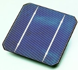
All Topics  
Solar cell


   Email Print
   Bookmark   Link


Solar cell


A solar cell or photovoltaic cell is a device that converts sunlight
Sunlight

Sunlight, in the broad sense, is the total spectroscopy of the electromagnetic radiation given off by the Sun. On Earth, sunlight is Filter ed through the Earth's atmosphere, and the solar radiation is obvious as daylight when the Sun is above the horizon....
 directly into electricity
Electricity

Electricity is a general term that encompasses a variety of phenomena resulting from the presence and flow of electric charge. These include many easily recognizable phenomena such as lightning and static electricity, but in addition, less familiar concepts such as the electromagnetic field and electromagnetic induction....
 by the photovoltaic effect. Sometimes the term solar cell is reserved for devices intended specifically to capture energy from sunlight, while the term photovoltaic cell is used when the source is unspecified. Assemblies of cells are used to make solar panels, solar modules, or photovoltaic array
Photovoltaic array

A photovoltaic array is a linked collection of photovoltaic modules, which are in turn made of multiple interconnected solar cells. The cells convert Solar power into direct current electricity via the photovoltaic effect....
s.


Discussion
Ask a question about 'Solar cell'
Start a new discussion about 'Solar cell'
Answer questions from other users
Full Discussion Forum


Recent Posts


Encyclopedia


A solar cell or photovoltaic cell is a device that converts sunlight
Sunlight

Sunlight, in the broad sense, is the total spectroscopy of the electromagnetic radiation given off by the Sun. On Earth, sunlight is Filter ed through the Earth's atmosphere, and the solar radiation is obvious as daylight when the Sun is above the horizon....
 directly into electricity
Electricity

Electricity is a general term that encompasses a variety of phenomena resulting from the presence and flow of electric charge. These include many easily recognizable phenomena such as lightning and static electricity, but in addition, less familiar concepts such as the electromagnetic field and electromagnetic induction....
 by the photovoltaic effect. Sometimes the term solar cell is reserved for devices intended specifically to capture energy from sunlight, while the term photovoltaic cell is used when the source is unspecified. Assemblies of cells are used to make solar panels, solar modules, or photovoltaic array
Photovoltaic array

A photovoltaic array is a linked collection of photovoltaic modules, which are in turn made of multiple interconnected solar cells. The cells convert Solar power into direct current electricity via the photovoltaic effect....
s. Photovoltaics
Photovoltaics

Photovoltaics is the field of technology and research related to the application of solar cells for energy by converting sunlight directly into electricity....
 is the field of technology and research related to the application of solar cells in producing electricity for practical use. The energy generated this way is an example of solar energy (also called solar power).

Solar Cell

History


The term "photovoltaic" comes from the Greek
Greek language

Greek is an Indo-European languages native to the southern Balkan peninsula, the language of the Greek people. It forms an independent branch within Indo-European....
 f?? (phos) meaning "light", and "voltaic", meaning electric, from the name of the Italian
Italian people

The Italian people are a Southern European ethnic group located primarily in Italy and, by virtue of a wide-ranging Italian diaspora, throughout Western Europe, the Americas and Australia....
 physicist Volta
Alessandro Volta

Count Alessandro Antonio Anastasio Volta was a Lombardy Physics known especially for the development of the first cell in 1800....
, after whom a unit of electrical potential, the volt
Volt

The volt is the SI SI derived unit of electric potential difference or electromotive force, commonly known as voltage. It is named in honor of the Lombard physicist Alessandro Volta , who invented the voltaic pile, possibly the first chemical battery ....
, is named. The term "photo-voltaic" has been in use in English since 1849.

The photovoltaic effect was first recognized in 1839 by French physicist A. E. Becquerel
A. E. Becquerel

Alexandre-Edmond Becquerel was a France physicist who studied the solar spectrum, magnetism, electricity, and optics. He is known for his work in luminescence and phosphorescence....
. However, it was not until 1883 that the first solar cell was built, by Charles Fritts
Charles Fritts

Charles Fritts was an American inventor credited with creating the first working solar cell in 1884.Fritts coated the semiconductor material selenium with an extremely thin layer of gold....
, who coated the semiconductor
Semiconductor

A semiconductor is a material that has electrical conductivity between those of a Electrical conductor and an electrical insulation; it can vary over that wide range either permanently or dynamically....
 selenium
Selenium

Selenium is a chemical element with the atomic number 34, represented by the chemical symbol Se, an atomic mass of 78.96. It is a nonmetal, chemically related to sulfur and tellurium, and rarely occurs in its elemental state in nature....
 with an extremely thin layer of gold
Gold

Gold is a chemical element with the symbol Au and atomic number 79. It is a highly sought-after precious metal, having been used as money, as a store of value, in jewelry, in sculpture, and for ornamentation since the beginning of recorded history....
 to form the junctions. The device was only around 1% efficient. Sven Ason Berglund had a number of patents concerning methods of increasing the capacity of these cells. Russell Ohl
Russell Ohl

Russell Ohl was an American engineer who is generally recognized for patenting the modern solar cell . Ohl was a notable semiconductor researcher prior to the invention of the transistor....
 patented the modern junction semiconductor solar cell in 1946 ("Light sensitive device"), which was discovered while working on the series of advances that would lead to the transistor
Transistor

In electronics, a transistor is a semiconductor device commonly used to Electronic amplifier or switch Electronics signals. A transistor is made of a solid piece of a semiconductor material, with at least three terminals for connection to an external circuit....
.

The modern age of solar power technology arrived in 1954 when Bell Laboratories, experimenting with semiconductors, accidentally found that silicon
Silicon

Silicon is the most common metalloid. It is a chemical element, which has the symbol Si and atomic number 14. The atomic mass is 28.0855....
 doped with certain impurities was very sensitive to light.Daryl Chapin, with Bell Labs colleagues Calvin Fuller and Gerald Pearson, invented the first practical device for converting sunlight into useful electrical power.This resulted in the production of the first practical solar cells with a sunlight energy conversion efficiency of around 6 percent.The solar battery was first demonstrated on April 25, 1954. The first spacecraft to use solar panels was the US satellite Vanguard 1
Vanguard 1

Vanguard 1 was the fourth artificial satellite launched, and is the oldest still orbiting Earth, though there is no longer any communication with it....
, launched in March 1958 with solar cells made by Hoffman Electronics
List of television manufacturers

This is a list of television manufacturers, past and present.References...
. This milestone created interest in producing and launching a geostationary communications satellite
Satellite

In the context of spaceflight, a satellite is an Physical body which has been placed into orbit by human endeavor. Such objects are sometimes called artificial satellites to distinguish them from natural satellites such as the Moon....
, in which solar energy would provide a viable power supply. This was a crucial development which stimulated funding from several governments into research for improved solar cells.

In 1970 the first highly effective GaAs
Gaas

Gaas is a Communes of France in the Landes Departments of France in Aquitaine in southwestern France....
 heterostructure solar cells were created by Zhores Alferov and his team in the USSR. Metal Organic Chemical Vapor Deposition (MOCVD, or OMCVD) production equipment was not developed until the early 1980s, limiting the ability of companies to manufacture the GaAs solar cell. In the United States, the first 17% efficient air mass zero (AM0
Air mass coefficient

The air mass coefficient characterizes the solar spectrum after the solar radiation has traveled through the atmosphere. It is commonly used to characterize the performance of solar cells under standardized conditions referred to as "AM" and a number....
) single-junction GaAs solar cells were manufactured in production quantities in 1988 by Applied Solar Energy Corporation (ASEC). The "dual junction" cell was accidentally produced in quantity by ASEC in 1989 as a result of the change from GaAs on GaAs substrates to GaAs on Germanium (Ge) substrates. The accidental doping of Ge with the GaAs buffer layer created higher open circuit voltages, demonstrating the potential of using the Ge substrate as another cell. As GaAs single-junction cells topped 19% AM0
Air mass coefficient

The air mass coefficient characterizes the solar spectrum after the solar radiation has traveled through the atmosphere. It is commonly used to characterize the performance of solar cells under standardized conditions referred to as "AM" and a number....
 production efficiency in 1993, ASEC developed the first dual junction cells for spacecraft use in the United States, with a starting efficiency of approximately 20%. These cells did not utilize the Ge as a second cell, but used another GaAs-based cell with different doping. Eventually GaAs dual junction cells reached production efficiencies of about 22%. Triple Junction solar cells began with AM0
Air mass coefficient

The air mass coefficient characterizes the solar spectrum after the solar radiation has traveled through the atmosphere. It is commonly used to characterize the performance of solar cells under standardized conditions referred to as "AM" and a number....
 efficiencies of approximately 24% in 2000, 26% in 2002, 28% in 2005, and in 2007 have evolved to a 30% AM0
Air mass coefficient

The air mass coefficient characterizes the solar spectrum after the solar radiation has traveled through the atmosphere. It is commonly used to characterize the performance of solar cells under standardized conditions referred to as "AM" and a number....
 production efficiency, currently in qualification.

Recent world record claims of efficiency for multiple junction solar cells are discussed in the Records section.

Three generations of solar cells


Solar Cells are classified into three generations which indicates the order of which each became important. At present there is concurrent research into all three generations while the first generation technologies are most highly represented in commercial production, accounting for 89.6% of 2007 production.

First Generation

First generation cells consist of large-area, high quality and single junction devices. First Generation technologies involve high energy and labor inputs which prevent any significant progress in reducing production costs. Single junction silicon devices are approaching the theoretical limiting efficiency of 33% and achieve cost parity with fossil fuel
Fossil fuel

Fossil fuels or mineral fuels are fossil source fuels, that is, carbon or hydrocarbons found in the earth?s Crust .Fossil fuel range from volatile materials with low carbon:hydrogen ratios like methane, to liquid petroleum to nonvolatile materials composed of almost pure carbon, like anthracite coal....
 energy generation after a payback period of 5-7 years. They are not likely to get lower than US$1/W.

Second Generation
Second generation materials have been developed to address energy requirements and production costs of solar cells. Alternative manufacturing techniques such as vapour deposition, electroplating
Electroplating

Electroplating is a plating process that uses electrical direct current to redox cations of a desired material from a solution and coat a electrical conductivity object with a thin layer of the material, such as a metal....
, and use of Ultrasonic Nozzle
Ultrasonic Nozzle

This type of spray nozzle utilizes high frequency vibration to produce nearly narrow drop size distribution and low velocity spray from a low viscosity liquid....
s are advantageous as they reduce high temperature processing significantly. It is commonly accepted that as manufacturing techniques evolve production costs will be dominated by constituent material requirements, whether this be a silicon
Silicon

Silicon is the most common metalloid. It is a chemical element, which has the symbol Si and atomic number 14. The atomic mass is 28.0855....
 substrate
Substrate (materials science)

Substrate is a term used in materials science to describe the base material on which processing is conducted to produce new film or layers of material such as deposited coatings....
, or glass cover. Second generation technologies are expected to gain market share in 2008.

Such processes can bring costs down to a little under US$0.50/W but because of the defects inherent in the lower quality processing methods, have much reduced efficiencies compared to First Generation.

The most successful second generation materials have been cadmium telluride
Cadmium telluride

Cadmium telluride is a crystalline Chemical compound formed from cadmium and tellurium with a zincblende .In the bulk crystalline form it is a direct bandgap semiconductor....
 (CdTe), copper indium gallium selenide
Copper indium gallium selenide

"Copper indium selenide" redirects here.Copper indium gallium selenide is a I-III-VI compound semiconductor material composed of copper, indium, gallium, and selenium....
, amorphous silicon
Amorphous silicon

Amorphous silicon is the non-crystalline allotropic form of silicon. Silicon is a four-fold coordinated atom that is normally tetrahedron bonded to four neighboring silicon atoms....
 and micromorphous silicon. These materials are applied in a thin film
Thin film

Thin films are thin material Layer s ranging from fractions of a nanometre to several micrometres in thickness. Electronics semiconductor devices and optical coatings are the main applications benefiting from thin film construction....
 to a supporting substrate such as glass or ceramics reducing material mass and therefore costs. These technologies do hold promise of higher conversion efficiencies, particularly CIGS-CIS
Copper indium gallium selenide

"Copper indium selenide" redirects here.Copper indium gallium selenide is a I-III-VI compound semiconductor material composed of copper, indium, gallium, and selenium....
, DSC and CdTe
Cadmium telluride

Cadmium telluride is a crystalline Chemical compound formed from cadmium and tellurium with a zincblende .In the bulk crystalline form it is a direct bandgap semiconductor....
 offers significantly cheaper production costs.

Among major manufacturers there is certainly a trend toward second generation technologies however commercialisation of these technologies has proven difficult. In 2007 First Solar
First Solar

First Solar, Inc. is a publicly-held U.S. energy company in the solar sector. It manufactures photovoltaic solar modules using a thin film semiconductor process based on Cadmium telluride, to produce photovoltaic modules....
 produced 200 MW of CdTe solar cells making it the fifth largest producer of solar cells in 2007 and the first ever to reach the top 10 from production of second generation technologies alone. Wurth Solar commercialised its CIS
Copper indium gallium selenide

"Copper indium selenide" redirects here.Copper indium gallium selenide is a I-III-VI compound semiconductor material composed of copper, indium, gallium, and selenium....
 technology in 2007 producing 15 MW. Nanosolar
Nanosolar

Nanosolar is a developer of solar power technology. Based in San Jose, California, CA, Nanosolar has developed and commercialized a low-cost printed electronics solar cell manufacturing process....
 commercialised its CIGS technology in 2007 with a production capacity of 430 MW for 2008 in the USA and Germany. , a Honda company, also began to their CIGS base solar panel in 2008.

In 2007 CdTe production represented 4.7% of total market share, thin-film silicon 5.2% and CIGS 0.5%.

Third Generation

Third generation technologies aim to enhance poor electrical performance of second generation (thin-film technologies) while maintaining very low production costs.

Current research is targeting conversion efficiencies of 30-60% while retaining low cost materials and manufacturing techniques. They can exceed the theoretical solar conversion efficiency limit for a single energy threshold material, that was calculated in 1961 by Shockley and Queisser as 31% under 1 sun
Sun unit

The sun unit is a measure of sun intensity weighted for skin damage related to the UV index....
 illumination and 40.8% under maximal concentration of sunlight (46,200 suns, which makes the latter limit more difficult to approach than the former).

There are a few approaches to achieving these high efficiencies:

  • Multijunction photovoltaic cell
    Multijunction photovoltaic cell

    Multijunction photovoltaic cells are a sub-class of solar cell or photovoltaic cell developed for higher efficiency. These multijunction cells consist of multiple thin films produced using molecular beam epitaxy and / or Metalorganic vapour phase epitaxy....
     (multiple energy threshold devices).
  • Modifying incident spectrum (concentration
    Concentration

    In chemistry, concentration is the measure of how much of a given chemical substance there is mixed with another substance. This can apply to any sort of chemical mixture, but most frequently the concept is limited to homogeneous solutions, where it refers to the amount of solute in the solvent....
    ).
  • Use of excess thermal generation (caused by UV light) to enhance voltages or carrier collection.
  • Use of infrared
    Infrared

    Infrared radiation is electromagnetic radiation whose wavelength is longer than that of visible light , but shorter than that of terahertz radiation and microwaves ....
     spectrum to produce electricity at night.


Technologies includes:

  • Silicon nanostructures
  • Up/Down converter
    Upconverter

    Upconverter can refer to:* Radio frequency upconverter* Video scaler...
    s
  • Hot-carrier cells
  • Thermoelectric cells


High efficiency cells


High efficiency solar cells are a class of solar cell
Solar cell

A solar cell or photovoltaic cell is a device that converts sunlight directly into electricity by the photovoltaic effect. Sometimes the term solar cell is reserved for devices intended specifically to capture energy from sunlight, while the term photovoltaic cell is used when the source is unspecified....
s that can generate electricity
Electricity

Electricity is a general term that encompasses a variety of phenomena resulting from the presence and flow of electric charge. These include many easily recognizable phenomena such as lightning and static electricity, but in addition, less familiar concepts such as the electromagnetic field and electromagnetic induction....
 at higher efficiencies than conventional solar cells. While high efficiency solar cells are more efficient in terms of electrical output per incident energy (watt/watt), much of the industry is focused on the most cost efficient technologies (cost-per-watt or $/watt). Still, many businesses and academics are focused on increasing the electrical efficiency of cells, and much development is focused on high efficiency solar cells.

Records


Monocrystalline Si
In 1994, the University of New South Wales (UNSW) reported the highest silicon solar cell efficiency of 24.7% with their PERL cell technology. This record has been valid until 2008.

UNSW's ARC Photovoltaic Centre of Excellence has reported the first silicon solar cell to achieve the milestone of 25 per cent efficiency.

Polycrystaline Si

Multiple junction solar cells
The record for multiple junction solar cells is disputed. A team lead by the University of Delaware, the Fraunhofer Institute, and NREL all claim the world record title at 42.8, 41.1, and 40.8 percent, respectively. NREL claims that the other implementations have never been put under any standardized tests and, in the case of the University of Delaware project, represents only hypothetical efficiencies of a panel that's never been fully assembled. However, NREL claims it is one of only three laboratories in the world capable of conducting valid tests. On the other hand the Fraunhofer Institute is among those three facilities.

Thin film solar cells
In 2002, the highest reported efficiency for solar cells based on thin films of CdTe
Cadmium telluride

Cadmium telluride is a crystalline Chemical compound formed from cadmium and tellurium with a zincblende .In the bulk crystalline form it is a direct bandgap semiconductor....
 is 18%, which was achieved by the research group of prof. I.M.Dharmadasa at Sheffield Hallam University
Sheffield Hallam University

Sheffield Hallam University is a Higher Education institution based in the South Yorkshire city of Sheffield, England. The university is based on two sites in Sheffield....
 in the United Kingdom
United Kingdom

The United Kingdom of Great Britain and Northern Ireland, commonly known as the United Kingdom , the UK or Britain,is a sovereign state located off the northwestern coast of continental Europe....
.

The US national renewable energy research facility NREL achieved an efficiency of 19.9% for the solar cells based on copper indium gallium selenide
Copper indium gallium selenide

"Copper indium selenide" redirects here.Copper indium gallium selenide is a I-III-VI compound semiconductor material composed of copper, indium, gallium, and selenium....
 thin films, also known as CIGS. These CIGS films have been grown by physical vapour deposition in a three-stage co-evaporation process. In this process In, Ga and Se are evaporated in the first step; in the second step it is followed by Cu and Se co-evaporation and in the last step terminated by In, Ga and Se evaporation again.

Applications and implementations

Polycristalline Silicon Wafer 20060626 568
Solar cells are often electrically connected and encapsulated as a module. PV modules often have a sheet of glass on the front (sun up) side, allowing light to pass while protecting the semiconductor wafers
Wafer (electronics)

A wafer is a thin slice of semiconductor material, such as a silicon crystal, used in the Semiconductor fabrication of integrated circuit and other microdevices....
 from the elements (rain
Rain

Rain is liquid precipitation . On Earth, it is the condensation of atmospheric water vapor into droplet heavy enough to fall, often making it to the surface....
, hail
Hail

Hail is a form of Precipitation which consists of balls or irregular lumps of ice . Hailstones on Earth usually consist mostly of ice and measure between 5 and 150 millimeters in diameter, with the larger stones coming from severe thunderstorms....
, etc.). Solar cells are also usually connected in series
Series and parallel circuits

In electronics, components of an electronic circuit can be connected in series or in parallel. Components connected in series are connected along a single path, so the same electric current flows through all of the components....
 in modules, creating an additive voltage
Voltage

Electrical tension is the potential difference between two points of an electrical or electronic circuit, expressed in volts. It is the measurement of the potential for an electric field to cause an electric current in an electrical conductor....
. Connecting cells in parallel will yield a higher current. Modules are then interconnected, in series or parallel, or both, to create an array with the desired peak DC voltage and current.

The power output of a solar array is measured in watt
WATT

WATT is a radio station broadcasting a News radio-Talk radio-Sports radio format. Licensed to Cadillac, Michigan, it first began broadcasting in 1945....
s or kilowatts. In order to calculate the typical energy needs of the application, a measurement in watt-hour
Watt-hour

The kilowatt hour, also written kilowatt-hour, is a unit of energy.Energy delivered by electric utilities is usually expressed and charged for in kWh....
s, kilowatt-hours or kilowatt-hours per day is often used. A common rule of thumb
Rule of thumb

A rule of thumb is a principle with broad application that is not intended to be strictly accurate or reliable for every situation. It is an easily learned and easily applied procedure for approximately calculating or recalling some value, or for making some determination....
 is that average power is equal to 20% of peak power, so that each peak kilowatt of solar array output power corresponds to energy production of 4.8 kWh per day (24 hours x 1kW x 20% = 4.8 kWh)

To make practical use of the solar-generated energy, the electricity is most often fed into the electricity grid using inverters (grid-connected PV systems); in stand alone systems, batteries are used to store the energy that is not needed immediately.

Theory


Simple explanation


  1. Photon
    Photon

    In physics, the photon is an elementary particle, the quantum of the electromagnetic field and the basic unit of light and all other forms of electromagnetic radiation....
    s in sunlight
    Sunlight

    Sunlight, in the broad sense, is the total spectroscopy of the electromagnetic radiation given off by the Sun. On Earth, sunlight is Filter ed through the Earth's atmosphere, and the solar radiation is obvious as daylight when the Sun is above the horizon....
     hit the solar panel and are absorbed by semiconducting materials, such as silicon
    Silicon

    Silicon is the most common metalloid. It is a chemical element, which has the symbol Si and atomic number 14. The atomic mass is 28.0855....
    .
  2. Electrons (negatively charged) are knocked loose from their atoms, allowing them to flow through the material to produce electricity
    Electricity

    Electricity is a general term that encompasses a variety of phenomena resulting from the presence and flow of electric charge. These include many easily recognizable phenomena such as lightning and static electricity, but in addition, less familiar concepts such as the electromagnetic field and electromagnetic induction....
    . Due to the special composition of solar cells, the electrons are only allowed to move in a single direction. The complementary positive charges that are also created (like bubbles) are called holes
    Electron hole

    An electron hole is the conceptual and mathematical opposite of an electron, useful in the study of physics and chemistry. The concept describes the lack of an electron....
     and flow in the direction opposite of the electrons in a silicon solar panel.
  3. An array of solar cells converts solar energy into a usable amount of direct current
    Direct current

    Direct current is the unidirectional flow of electric charge. Direct current is produced by such sources as battery , thermocouples, solar cells, and commutator-type electric machines of the dynamo type....
     (DC) electricity.


Photogeneration of charge carriers


When a photon
Photon

In physics, the photon is an elementary particle, the quantum of the electromagnetic field and the basic unit of light and all other forms of electromagnetic radiation....
 hits a piece of silicon, one of three things can happen:

  1. the photon can pass straight through the silicon — this (generally) happens for lower energy photons,
  2. the photon can reflect off the surface,
  3. the photon can be absorbed by the silicon, if the photon energy is higher than the silicon band gap
    Band gap

    In solid state physics and related applied fields, a band gap, also called an energy gap or bandgap, is an energy range in a solid where no electron states exist....
     value. This generates an electron-hole pair and sometimes heat, depending on the band structure.


When a photon is absorbed, its energy is given to an electron in the crystal lattice. Usually this electron is in the valence band
Valence band

In solids, the valence band is the highest range of electron energy where electrons are normally present at absolute zero.In semiconductors and Electrical insulations, there is a band gap above the valence band, followed by a conduction band above that....
, and is tightly bound in covalent bonds between neighboring atoms, and hence unable to move far. The energy given to it by the photon "excites" it into the conduction band
Conduction band

In the physics field of semiconductors and Electrical insulations, the conduction band is the range of electron energy, higher than that of the valence band, sufficient to make the electrons free to accelerate under the influence of an applied electric field and thus constitute an electric current....
, where it is free to move around within the semiconductor. The covalent bond that the electron was previously a part of now has one fewer electron — this is known as a hole. The presence of a missing covalent bond allows the bonded electrons of neighboring atoms to move into the "hole," leaving another hole behind, and in this way a hole can move through the lattice. Thus, it can be said that photons absorbed in the semiconductor create mobile electron-hole pairs.

A photon need only have greater energy than that of the band gap in order to excite an electron from the valence band into the conduction band. However, the solar frequency spectrum
Frequency spectrum

Familiar concepts associated with a frequency are colors, musical notes, radio/TV channels, and even the regular rotation of the earth. A source of light can have many colors mixed together and in different amounts ....
 approximates a black body
Black body

In physics, a black body is an Physical body that absorbs all electromagnetic radiation that falls on it. No electromagnetic radiation passes through it and none is Reflection ....
 spectrum at ~6000 K, and as such, much of the solar radiation reaching the Earth
Earth

Earth is the third planet from the Sun. Earth is the largest of the terrestrial planets in the Solar System in diameter, mass and density. It is also referred to as the World and Wiktionary:Terra.Note that by International Astronomical Union convention, the term "Terra" is used for naming extensive land masses, rather...
 is composed of photons with energies greater than the band gap of silicon. These higher energy photons will be absorbed by the solar cell, but the difference in energy between these photons and the silicon band gap is converted into heat (via lattice vibrations — called phonons) rather than into usable electrical energy.

Charge carrier separation

There are two main modes for charge carrier separation in a solar cell:

  1. drift of carriers, driven by an electrostatic field established across the device
  2. diffusion of carriers from zones of high carrier concentration to zones of low carrier concentration (following a gradient of electrochemical potential).


In the widely used p-n junction
P-n junction

A p-n junction is a junction formed by combining P-type semiconductor and N-type semiconductor semiconductors together in very close contact.The term junction refers to the region where the two regions of the semiconductor meet....
 solar cells, the dominant mode of charge carrier separation is by drift. However, in non-p-n-junction solar cells (typical of the third generation solar cell
Third generation solar cell

Third generation photovoltaic cell, also called advanced thin-film photovoltaic cell, is a range of novel alternatives to "first generation" and "second generation" cells....
 research such as dye and polymer solar cell
Polymer solar cell

Polymer solar cells are a type of organic solar cell , or organic photovoltaic cell that produce electricity from sunlight using polymers. It is a relatively novel technology, they are being researched by universities, national laboratories and several companies around the world....
s), a general electrostatic field has been confirmed to be absent, and the dominant mode of separation is via charge carrier diffusion.

The p-n junction


The most commonly known solar cell is configured as a large-area p-n junction
P-n junction

A p-n junction is a junction formed by combining P-type semiconductor and N-type semiconductor semiconductors together in very close contact.The term junction refers to the region where the two regions of the semiconductor meet....
 made from silicon. As a simplification, one can imagine bringing a layer of n-type silicon into direct contact with a layer of p-type silicon. In practice, p-n junctions of silicon solar cells are not made in this way, but rather, by diffusing an n-type dopant into one side of a p-type wafer (or vice versa).

If a piece of p-type silicon is placed in intimate contact with a piece of n-type silicon, then a diffusion
Diffusion

Molecular diffusion, often called simply diffusion, is a net transport of molecules from a region of higher concentration to one of lower concentration by random molecular motion....
 of electrons occurs from the region of high electron concentration (the n-type side of the junction) into the region of low electron concentration (p-type side of the junction). When the electrons diffuse across the p-n junction, they recombine with holes on the p-type side. The diffusion of carriers does not happen indefinitely however, because of an electric field
Electric field

In physics, the space surrounding an electric charge or in the presence of a time-varying magnetic field has a property called an electric field ....
 which is created by the imbalance of charge immediately on either side of the junction which this diffusion creates. The electric field established across the p-n junction creates a diode
Diode

In electronics, a diode is a two-terminal device .Diodes have two active electrodes between which the signal of interest may flow, and most are used for their unidirectional electric current property....
 that promotes current
Electric current

Electric current is the flow of electric charge. The electric charge may be either electrons or ions.The International System of Units unit of electric current intensity is the ampere....
 in only one direction across the junction. Electrons may pass from the n-type side into the p-type side, and holes may pass from the p-type side to the n-type side, but not the other way around. This region where electrons have diffused across the junction is called the depletion region because it no longer contains any mobile charge carriers. It is also known as the "space charge region".

Connection to an external load

Ohmic
Ohmic contact

An ohmic contact is a region on a semiconductor device that has been prepared so that the Current-voltage characteristic curve of the device is linear and symmetric....
 metal
Metal

In chemistry, a metal is a chemical element whose atoms readily lose electrons to form positive ions , and form metallic bonds between other metal atoms and ionic bonds between nonmetal atoms....
-semiconductor contacts are made to both the n-type and p-type sides of the solar cell, and the electrodes connected to an external load. Electrons that are created on the n-type side, or have been "collected" by the junction and swept onto the n-type side, may travel through the wire, power the load, and continue through the wire until they reach the p-type semiconductor-metal contact. Here, they recombine with a hole that was either created as an electron-hole pair on the p-type side of the solar cell, or are swept across the junction from the n-type side after being created there.

The voltage measured is equal to the difference in the quasi Fermi levels of the minority carriers ie. electrons in the p-type portion, and holes in the n-type portion.

Equivalent circuit of a solar cell


To understand the electronic behavior of a solar cell, it is useful to create a model
Model (physical)

A physical model is a smaller or larger physical copy of an object. The object being modelled may be small or large .The geometry of the model and the object it represents are often similar in the sense that one is a rescaling of the other; in such cases the Scale is an important characteristic....
 which is electrically equivalent, and is based on discrete electrical components whose behavior is well known. An ideal solar cell may be modelled by a current source in parallel with a diode
Diode

In electronics, a diode is a two-terminal device .Diodes have two active electrodes between which the signal of interest may flow, and most are used for their unidirectional electric current property....
; in practice no solar cell is ideal, so a shunt resistance and a series resistance component are added to the model. The resulting equivalent circuit of a solar cell is shown on the left. Also shown, on the right, is the schematic representation of a solar cell for use in circuit diagrams.

Characteristic equation

From the equivalent circuit it is evident that the current produced by the solar cell is equal to that produced by the current source, minus that which flows through the diode, minus that which flows through the shunt resistor:

where
  • = output current (amperes)
  • = photogenerated current (amperes)
  • = diode current (amperes)
  • = shunt current (amperes)


The current flowing through these elements governed by the voltage across them:

where
  • = voltage across the output terminals (volts)
  • = output current (amperes)
  • = series resistance (O
    O

    O is the fifteenth letter of the modern Latin alphabet. Its name in English language is spelled o , plural oes ....
    )


By the Shockley diode equation
Diode

In electronics, a diode is a two-terminal device .Diodes have two active electrodes between which the signal of interest may flow, and most are used for their unidirectional electric current property....
, the current diverted through the diode is:

where
  • = reverse saturation current
    Saturation current

    Saturation current is a term used to describe a limit to the amount of electrical current that can flow in an electronic circuit or device. As the voltage applied to a circuit is increased, the current flow will increase proportionately until the saturation current is achieved, at which point the excess current can no longer flow, and is ins...
     (amperes)
  • = diode ideality factor (1 for an ideal diode)
  • = elementary charge
    Elementary charge

    The elementary charge, usually denoted e, is the electric charge carried by a single proton, or equivalently, the negative of the electric charge carried by a single electron....
  • = Boltzmann's constant
  • = absolute temperature
  • For silicon at 25°C, volts.


By Ohm's law
Ohm's law

Ohm's law applies to electrical circuits; it states that the electric current through a conductor between two points is directly Proportionality to the potential difference or voltage across the two points, and inversely proportional to the Electrical resistance between them....
, the current diverted through the shunt resistor is:

where
  • = shunt resistance (O)


Substituting these into the first equation produces the characteristic equation of a solar cell, which relates solar cell parameters to the output current and voltage:

An alternative derivation produces an equation similar in appearance, but with on the left-hand side. The two alternatives are identities; that is, they yield precisely the same results.

In principle, given a particular operating voltage the equation may be solved to determine the operating current at that voltage. However, because the equation involves on both sides in a transcendental function
Transcendental function

A transcendental function is a function that does not satisfy a polynomial equation whose coefficients are themselves polynomials, in contrast to an algebraic function, which does satisfy such an equation....
 the equation has no general analytical solution. However, even without a solution it is physically instructive. Furthermore, it is easily solved using numerical methods. (A general analytical solution to the equation is possible using Lambert's W function, but since Lambert's W generally itself must be solved numerically this is a technicality.)

Since the parameters , , , and cannot be measured directly, the most common application of the characteristic equation is nonlinear regression
Nonlinear regression

In statistics, nonlinear regression is a form of regression analysis in which observational data are modeled by a function which is a nonlinear combination of the model parameters and depends on one or more independent variables....
 to extract the values of these parameters on the basis of their combined effect on solar cell behavior.

Effect of physical size

The values of , , and are dependent upon the physical size of the solar cell. In comparing otherwise identical cells, a cell with twice the surface area of another will, in principle, have double the because it has twice the junction area across which current can leak. It will also have half the and because it has twice the cross-sectional area through which current can flow. For this reason, the characteristic equation is frequently written in terms of current density
Current density

Current density is a measure of the density of flow of a conserved charge . Usually the charge is the electric charge, in which case the associated current density is the electric current per unit area of cross section, but the term current density can also be applied to other conserved quantities....
, or current produced per unit cell area:

where
  • = current density (amperes/cm2)
  • = photogenerated current density (amperes/cm2)
  • = reverse saturation current density (amperes/cm2)
  • = specific series resistance (O-cm2)
  • = specific shunt resistance (O-cm2)


This formulation has several advantages. One is that since cell characteristics are referenced to a common cross-sectional area they may be compared for cells of different physical dimensions. While this is of limited benefit in a manufacturing setting, where all cells tend to be the same size, it is useful in research and in comparing cells between manufacturers. Another advantage is that the density equation naturally scales the parameter values to similar orders of magnitude, which can make numerical extraction of them simpler and more accurate even with naive solution methods.

A practical limitation of this formulation is that as cell sizes shrink, certain parasitic effects grow in importance and can affect the extracted parameter values. For example, recombination and contamination of the junction tend to be greatest at the perimeter of the cell, so very small cells may exhibit higher values of or lower values of than larger cells that are otherwise identical. In such cases, comparisons between cells must be made cautiously and with these effects in mind.

Cell temperature

Temperature affects the characteristic equation in two ways: directly, via in the exponential term, and indirectly via its effect on . (Strictly speaking, temperature affects all of the terms, but these two far more significantly than the others.) While increasing reduces the magnitude of the exponent in the characteristic equation, the value of increases in proportion to . The net effect is to reduce linearly with increasing temperature. The magnitude of this reduction is inversely proportional to ; that is, cells with higher values of suffer smaller reductions in voltage with increasing temperature. For most crystalline silicon solar cells the reduction is about 0.50%/°C, though the rate for the highest-efficiency crystalline silicon cells is around 0.35%/°C. By way of comparison, the rate for amorphous silicon solar cells is 0.20-0.30%/°C, depending on how the cell is made.

The amount of photogenerated current increases slightly with increasing temperature because of an increase in the number of thermally generated carriers in the cell. This effect is slight, however: about 0.065%/°C for crystalline silicon cells and 0.09% for amorphous silicon cells.

The overall effect of temperature on cell efficiency can be computed using these factors in combination with the characteristic equation. However, since the change in voltage is much stronger than the change in current, the overall effect on efficiency tends to be similar to that on voltage. Most crystalline silicon solar cells decline in efficiency by 0.50%/°C and most amorphous cells decline by 0.15-0.25%/°C. The figure to the right shows I-V curves that might typically be seen for a crystalline silicon solar cell at various temperatures.

Series resistance

As series resistance increases, the voltage drop between the junction voltage and the terminal voltage becomes greater for the same flow of current. The result is that the current-controlled portion of the I-V curve begins to sag toward the origin, producing a significant decrease in the terminal voltage and a slight reduction in . Very high values of will also produce a significant reduction in ; in these regimes, series resistance dominates and the behavior of the solar cell resembles that of a resistor. These effects are shown for crystalline silicon solar cells in the I-V curves displayed in the figure to the right.

Shunt resistance

As shunt resistance decreases, the flow of current diverted through the shunt resistor increases for a given level of junction voltage. The result is that the voltage-controlled portion of the I-V curve begins to sag toward the origin, producing a significant decrease in the terminal current and a slight reduction in . Very low values of will produce a significant reduction in . Much as in the case of a high series resistance, a badly shunted solar cell will take on operating characteristics similar to those of a resistor. These effects are shown for crystalline silicon solar cells in the I-V curves displayed in the figure to the right.

Reverse saturation current

If one assumes infinite shunt resistance, the characteristic equation can be solved for :

Thus, an increase in produces a reduction in proportional to the inverse of the logarithm of the increase. This explains mathematically the reason for the reduction in that accompanies increases in temperature described above. The effect of reverse saturation current on the I-V curve of a crystalline silicon solar cell are shown in the figure to the right. Physically, reverse saturation current is a measure of the "leakage" of carriers across the p-n junction in reverse bias. This leakage is a result of carrier recombination in the neutral regions on either side of the junction.

Ideality factor

The ideality factor (also called the emissivity factor) is a fitting parameter that describes how closely the diode's behavior matches that predicted by theory, which assumes the p-n junction of the diode is an infinite plane and no recombination occurs within the space-charge region. A perfect match to theory is indicated when . When recombination in the space-charge region dominate other recombination, however, . The effect of changing ideality factor independently of all other parameters is shown for a crystalline silicon solar cell in the I-V curves displayed in the figure to the right.

Most solar cells, which are quite large compared to conventional diodes, well approximate an infinite plane and will usually exhibit near-ideal behavior under Standard Test Condition . Under certain operating conditions, however, device operation may be dominated by recombination in the space-charge region. This is characterized by a significant increase in as well as an increase in ideality factor to . The latter tends to erode solar cell output voltage while the former acts to increase it. The net effect, therefore, is a combination of the increase in voltage shown for increasing in the figure to the right and the decrease in voltage shown for increasing in the figure above. Typically, is the more significant factor and the result is a reduction in voltage.

Solar cell efficiency factors


Energy conversion efficiency


A solar cell's energy conversion efficiency ("eta"), is the percentage of power converted (from absorbed light to electrical energy) and collected, when a solar cell is connected to an electrical circuit. This term is calculated using the ratio of the maximum power point, Pm, divided by the input light irradiance
Irradiance

Irradiance, radiant emittance, and radiant exitance are radiometry terms for the power of electromagnetic radiation at a surface, per unit area....
 (E, in W/m2) under standard test conditions (STC) and the surface area of the solar cell (Ac in m2).

STC specifies a temperature of 25°C and an irradiance of 1000 W/m2 with an air mass 1.5 (AM1.5) spectrum. These correspond to the irradiance and spectrum of sunlight incident on a clear day upon a sun-facing 37°-tilted surface with the sun at an angle of 41.81° above the horizon. This condition approximately represents solar noon near the spring and autumn equinoxes in the continental United States with surface of the cell aimed directly at the sun. Thus, under these conditions a solar cell of 12% efficiency with a 100 cm2 (0.01 m2) surface area can be expected to produce approximately 1.2 watts of power.

The losses of a solar cell may be broken down into reflectance losses, thermodynamic efficiency, recombination losses and resistive electrical loss. The overall efficiency is the product of each of these individual losses.

Due to the difficulty in measuring these parameters directly, other parameters are measured instead: Thermodynamic Efficiency, Quantum Efficiency, VOC ratio, and Fill Factor. Reflectance losses are a portion of the Quantum Efficiency under "External Quantum Efficiency". Recombination losses make up a portion of the Quantum Efficiency, VOC ratio, and Fill Factor. Resistive losses are predominantly categorized under Fill Factor, but also make up minor portions of the Quantum Efficiency, VOC ratio.

Generally, solar cells on the market today do not produce much electricity from ultraviolet
Ultraviolet

Ultraviolet light is electromagnetic radiation with a wavelength shorter than that of visible light, but longer than x-rays, in the range 400 nanometer to 10 nm, and energies from 3 Electron volt to 124 eV....
 light, instead it is either filtered out or absorbed by the cell, heating the cell. That heat is wasted energy and could even lead to damage to the cell.

Thermodynamic Efficiency Limit


Solar cells operate as quantum energy conversion devices, and are therefore subject to the "Thermodynamic Efficiency Limit". Photons with an energy below the band gap of the absorber material cannot generate a hole-electron pair, and so their energy is not converted to useful output and only generates heat if absorbed. For photons with an energy above the band gap energy, only a fraction of the energy above the band gap can be converted to useful output. When a photon of greater energy is absorbed, the excess energy above the band gap is converted to kinetic energy of the carrier combination. The excess kinetic energy is converted to heat through phonon interactions as the kinetic energy of the carriers slows to equilibrium velocity.

Solar cells with multiple band gap absorber materials are able to more efficiently convert the solar spectrum. By using multiple band gaps, the solar spectrum may be broken down into smaller bins where the thermodynamic efficiency limit is higher for each bin.

Quantum efficiency


As described above, when a photon is absorbed by a solar cell it can produce a pair of free charge carriers, i.e. an electron-hole pair. One of the carriers (the minority carrier) may then be able to reach the p-n junction and contribute to the current produced by the solar cell; such a carrier is said to be collected. Alternatively, the carrier may give up its energy and once again become bound to an atom within the solar cell without being collected; this process is then called recombination
Carrier generation and recombination

In the solid state physics of semiconductors, carrier generation and recombination are processes by which mobile charge carrier s are created and eliminated....
 since one electron and one hole recombine and thereby annihilate the associated free charge. The carriers that recombine do not contribute to the generation of electrical current.

Quantum efficiency
Quantum efficiency

Quantum efficiency is a quantity defined for a photosensitive device such as photographic film or a charge-coupled device as the percentage of photons hitting the photoreactive surface that will produce an electron?hole pair....
 refers to the percentage of photons that are converted to electric current (i.e., collected carriers) when the cell is operated under short circuit conditions. External quantum efficiency (EQE) is the fraction of incident photons that are converted to electrical current, while internal quantum efficiency (IQE) is the fraction of absorbed photons that are converted to electrical current. Mathematically, internal quantum efficiency is related to external quantum efficiency by the reflectance (R) and the transmittance (T) of the solar cell by . Please note that for a thick bulk Si solar cell T is approximately zero and is therefore in practical cases often neglected.

Quantum efficiency should not be confused with energy conversion efficiency
Energy conversion efficiency

File:Efficiency diagram by Zureks.svgEnergy conversion efficiency is the ratio between the useful output of an energy conversion machine and the input, in energy terms....
, as it does not convey information about the fraction of power that is converted by the solar cell. Furthermore, quantum efficiency is most usefully expressed as a spectral measurement (that is, as a function of photon wavelength or energy). Since some wavelengths are absorbed more effectively than others in most semiconductors, spectral measurements of quantum efficiency can yield valuable information about which parts of a particular solar cell design are most in need of improvement. Spectral quantum efficiency measurements also allow determining important solar cell parameters such as the base diffusion length.

Maximum-power point

A solar cell may operate over a wide range of voltage
Voltage

Electrical tension is the potential difference between two points of an electrical or electronic circuit, expressed in volts. It is the measurement of the potential for an electric field to cause an electric current in an electrical conductor....
s (V) and currents (I). By increasing the resistive load on an irradiated cell continuously from zero (a short circuit
Short circuit

A short circuit in an electrical circuit that allows a Electric current along a different path from the one intended.The electrical opposite of a short circuit is an "open circuit", which is an infinite resistance between two nodes....
) to a very high value (an open circuit
Open circuit

The term Open circuit may refer to:*Open-circuit voltage, the difference of electrical potential between two terminals of a device when there is no external load connected...
) one can determine the maximum-power
Maximum power theorem

In electrical engineering, the maximum power theorem states that, to obtain maximum external power from a source with a finite internal electrical resistance, the resistance of the load must be made the same as that of the source....
 point, the point that maximizes V×I; that is, the load for which the cell can deliver maximum electrical power at that level of irradiation. (The output power is zero in both the short circuit and open circuit extremes).

A high quality, monocrystalline silicon solar cell, at 25 °C cell temperature, may produce 0.60 volts open-circuit (Voc). The cell temperature in full sunlight, even with 25 °C air temperature, will probably be close to 45 °C, reducing the open-circuit voltage to 0.55 volts per cell. The voltage drops modestly, with this type of cell, until the short-circuit current is approached (Isc). Maximum power (with 45 °C cell temperature) is typically produced with 75% to 80% of the open-circuit voltage (0.43 volts in this case) and 90% of the short-circuit current. This output can be up to 70% of the Voc x Isc product. The short-circuit current (Isc) from a cell is nearly proportional to the illumination, while the open-circuit voltage (Voc) may drop only 10% with a 80% drop in illumination. Lower-quality cells have a more rapid drop in voltage with increasing current and could produce only 1/2 Voc at 1/2 Isc. The usable power output could thus drop from 70% of the Voc x Isc product to 50% or even as little as 25%. Vendors who rate their solar cell "power" only as Voc x Isc, without giving load curves, can be seriously distorting their actual performance.

The maximum power point of a photovoltaic varies with incident illumination. For systems large enough to justify the extra expense, a maximum power point tracker
Maximum power point tracker

A maximum power point tracker is a high efficiency DC to DC converter which functions as an optimal electrical load for a solar cell, most commonly for a Photovoltaic module or array, and converts the power to a voltage or current level which is more suitable to whatever load the system is designed to drive....
 tracks the instantaneous power by continually measuring the voltage
Voltage

Electrical tension is the potential difference between two points of an electrical or electronic circuit, expressed in volts. It is the measurement of the potential for an electric field to cause an electric current in an electrical conductor....
 and current
Electric current

Electric current is the flow of electric charge. The electric charge may be either electrons or ions.The International System of Units unit of electric current intensity is the ampere....
 (and hence, power transfer), and uses this information to dynamically adjust the load so the maximum power is always transferred, regardless of the variation in lighting.

Fill factor

Another defining term in the overall behavior of a solar cell is the fill factor
Fill factor

Fill factor in the context of solar cell technology it is defined as the ratio of the actual maximum obtainable power , to the theoretical power, ....
 (FF). This is the ratio of the maximum power point divided by the open circuit voltage (Voc) and the short circuit current (Isc):

The fill factor is directly affected by the values of the cells series and shunt resistance. Increasing the shunt resistance (Rsh) and decreasing the series resistance (Rs) will lead to higher fill factor, thus resulting in greater efficiency, and pushing the cells output power closer towards its theoretical maximum.

Comparison of energy conversion efficiencies


At this point, discussion of the different ways to calculate efficiency for space cells and terrestrial cells is necessary to alleviate confusion. In space, where there is no atmosphere, the spectrum of the sun is relatively unfiltered. However, on earth, with air filtering the incoming light, the solar spectrum changes. To account for the spectral differences, a system was devised to calculate this filtering effect. Simply, the filtering effect ranges from Air Mass
Air mass coefficient

The air mass coefficient characterizes the solar spectrum after the solar radiation has traveled through the atmosphere. It is commonly used to characterize the performance of solar cells under standardized conditions referred to as "AM" and a number....
 0 (AM0) in space, to approximately Air Mass 1.5 on earth. Multiplying the spectral differences by the quantum efficiency of the solar cell in question will yield the efficiency of the device. For example, a Silicon solar cell in space might have an efficiency of 14% at AM0, but have an efficiency of 16% on earth at AM 1.5. Terrestrial efficiencies typically are greater than space efficiencies.

Solar cell efficiencies vary from 6% for amorphous silicon-based solar cells to 40.7% with multiple-junction research lab cells and 42.8% with multiple dies assembled into a hybrid package. Solar cell energy conversion efficiencies for commercially available multicrystalline Si solar cells are around 14-19%. The highest efficiency cells have not always been the most economical — for example a 30% efficient multijunction cell based on exotic materials such as gallium arsenide or indium selenide and produced in low volume might well cost one hundred times as much as an 8% efficient amorphous silicon cell in mass production, while only delivering about four times the electrical power.

However, there is a way to "boost" solar power. By increasing the light intensity, typically photogenerated carriers are increased, resulting in increased efficiency by up to 15%. These so-called "concentrator systems" have only begun to become cost-competitive as a result of the development of high efficiency GaAs cells. The increase in intensity is typically accomplished by using concentrating optics. A typical concentrator system may use a light intensity 6-400 times the sun, and increase the efficiency of a one sun GaAs cell from 31% at AM 1.5 to 35%. See Solar_cell#Concentrating photovoltaics (CPV)
Solar cell

A solar cell or photovoltaic cell is a device that converts sunlight directly into electricity by the photovoltaic effect. Sometimes the term solar cell is reserved for devices intended specifically to capture energy from sunlight, while the term photovoltaic cell is used when the source is unspecified....
 below and Concentrating solar power (CSP).

A common method used to express economic costs of electricity-generating systems is to calculate a price per delivered kilowatt-hour (kWh). The solar cell efficiency in combination with the available irradiation has a major influence on the costs, but generally speaking the overall system efficiency is important. Using the commercially available solar cells (as of 2006) and system technology leads to system efficiencies between 5 and 19%. As of 2005, photovoltaic electricity generation costs ranged from ~0.60 US$/kWh (0.50 €/kWh) (central Europe) down to ~0.30 US$/kWh (0.25 €/kWh) in regions of high solar irradiation. This electricity is generally fed into the electrical grid on the customer's side of the meter. The cost can be compared to prevailing retail electric pricing (as of 2005), which varied from between 0.04 and 0.50 US$/kWh worldwide. (Note: in addition to solar irradiance profiles, these costs/kwh calculations will vary depending on assumptions for years of useful life of a system. Most c-Si panels are warranted for 25 years and should see 35+ years of useful life.)

The chart at the right illustrates the various commercial large-area module energy conversion efficiencies and the best laboratory efficiencies obtained for various materials and technologies.

Watts peak

Since solar cell output power depends on multiple factors, such as the sun
Sun

The Sun , a G V star, is the star at the center of the Solar System. The Earth and other matter orbit the Sun, which by itself accounts for about 98.6% of the Solar System's mass....
's incidence angle, for comparison purposes between different cells and panels, the measure of watts peak (Wp) is used. It is the output power under these conditions known as STC: Larger panels use the same rating system, but use kWp (1000 watts peak).

  1. insolation
    Insolation

    Insolation is a measure of solar radiation energy received on a given surface area in a given time. It is commonly expressed as average irradiance in watts per square meter or kilowatt-hours per square meter per day ....
     (solar irradiance
    Irradiance

    Irradiance, radiant emittance, and radiant exitance are radiometry terms for the power of electromagnetic radiation at a surface, per unit area....
    ) 1000 W/m2
  2. solar reference spectrum AM (airmass
    Airmass

    In astronomy, airmass is the optical path length through Earth's atmosphere for light from a celestial source. As it passes through the atmosphere, light is attenuated by scattering and absorption ; the more atmosphere through which it passes, the greater the attenuation....
    ) 1.5
  3. cell temperature 25°C


Solar cells and energy payback

Energy payback is the recovery (period) of the energy spent for manufacturing of the respective technical energy systems, also called harvesting ratio (ISO 13602).

In the 1990s, when silicon cells were twice as thick, efficiencies were 30% lower than today and lifetimes were shorter, it may well have cost more energy to make a cell than it could generate in a lifetime. In the meantime, the technology has progressed significantly, and the energy payback time of a modern photovoltaic module is typically from 1 to 4 years depending on the type and where it is used (see net energy gain
Net energy gain

Net Energy Gain is a concept used in energy economics that refers to the difference between the energy expended to harvest an energy source and the amount of energy gained from that harvest....
). Generally, thin film technologies - despite having comparatively low conversion efficiencies - achieve significantly shorter energy payback times than conventional systems (often < 1 year). With a typical lifetime of 20 to 30 years, this means that modern solar cells are net energy producers, i.e. they generate significantly more energy over their lifetime than the energy expended in producing them.

Light-absorbing materials


All solar cells require a light absorbing material
Absorption (electromagnetic radiation)

In physics, absorption of electromagnetic radiation is the way by which the energy of a photon is taken up by matter, typically the electrons of an atom....
 contained within the cell structure to absorb photons and generate electrons via the photovoltaic effect. The materials used in solar cells tend to have the property of preferentially absorbing the wavelengths of solar light that reach the earth surface; however, some solar cells are optimized for light absorption beyond Earth's atmosphere as well. Light absorbing materials can often be used in multiple physical configurations to take advantage of different light absorption and charge separation mechanisms.

Photovoltaic panels are normally made of either silicon or thin-film cells:

Many currently available solar cells are configured as bulk materials that are subsequently cut into wafers and treated in a "top-down" method of synthesis (silicon being the most prevalent bulk material).

Other materials are configured as thin-films (inorganic layer
Layer

Layer may refer to:* A layer of archaeological deposits in an excavation* A layer hen, a hen raised to produce eggs* Stratum, a layer of rock or soil with internally consistent characteristics...
s, organic dye
Dye

A dye can generally be described as a colored substance that has an Chemical affinity to the Wiktionary:substrate to which it is being applied....
s, and organic polymer
Polymer

A polymer is a large molecule composed of repeating structural units typically connected by covalent chemical bonds. While polymer in popular usage suggests plastic, the term actually refers to a large class of natural and synthetic materials with a variety of properties....
s) that are deposited on supporting substrates, while a third group are configured as nanocrystals and used as quantum dots (electron-confined nanoparticle
Nanoparticle

In nanotechnology, a particle is defined as a small object that behaves as a whole unit in terms of its transport and properties. It is further classified according to size: In terms of diameter, fine particles cover a range between 100 and 2500 nanometre, while ultrafine particles, on the other hand, are sized between 1 and 100 nanometers....
s) embedded in a supporting matrix in a "bottom-up" approach. Silicon remains the only material that is well-researched in both bulk (also called wafer-based) and thin-film configurations.

There are many new alternatives to Silicon photocells. Proprietary nanoparticle silicon printing processes promises many of the photovoltaic features that conventional silicon can never achieve. It can be printed reel-to-reel on stainless steel
Stainless steel

In metallurgy, stainless steel is defined as a steel alloy with a minimum of 10% chromium content by mass. Stainless steel does not stain, corrode, or rust as easily as ordinary steel , but it is not stain-proof....
 or other high temperature substrates. However, most of the work on the next generation of photovoltaics is directed at printing onto low cost flexible polymer film and ultimately on common packaging materials. The main contenders are currently CIGS
Copper indium gallium selenide

"Copper indium selenide" redirects here.Copper indium gallium selenide is a I-III-VI compound semiconductor material composed of copper, indium, gallium, and selenium....
, CdTe
Cadmium telluride

Cadmium telluride is a crystalline Chemical compound formed from cadmium and tellurium with a zincblende .In the bulk crystalline form it is a direct bandgap semiconductor....
, DSSC and organic photovoltaics.

The following is a current list of light absorbing materials, listed by configuration and substance-name:

Bulk


These bulk technologies are often referred to as wafer-based manufacturing. In other words, in each of these approaches, self-supporting wafers between 180 to 240 micrometers thick are processed and then soldered together to form a solar cell module. A general description of silicon wafer processing is provided in Manufacture and Devices.

Crystalline silicon

By far, the most prevalent bulk material for solar cells is crystalline silicon
Silicon

Silicon is the most common metalloid. It is a chemical element, which has the symbol Si and atomic number 14. The atomic mass is 28.0855....
 (abbreviated as a group as c-Si), also known as "solar grade silicon". Bulk silicon is separated into multiple categories according to crystallinity and crystal size in the resulting ingot
Ingot

An ingot is a material, usually metal, that is Casting into a shape suitable for further processing. It requires a second procedure of shaping, by means of cold/hot working to produce the final product....
, ribbon
Ribbon

A ribbon or riband is a thin band of flexible material, typically cloth but also plastic or sometimes metal, used primarily for binding and tying....
, or wafer
Wafer (electronics)

A wafer is a thin slice of semiconductor material, such as a silicon crystal, used in the Semiconductor fabrication of integrated circuit and other microdevices....
.

  1. monocrystalline silicon (c-Si): often made using the Czochralski process
    Czochralski process

    The Czochralski process is a method of crystal growth used to obtain single crystals of semiconductors , metals , salts, and synthetic gemstones....
    . Single-crystal wafer cells tend to be expensive, and because they are cut from cylindrical ingots, do not completely cover a square solar cell module without a substantial waste of refined silicon. Hence most c-Si panels have uncovered gaps at the four corners of the cells.
    Ribbon silicon is a type of monocrystalline silicon: it is formed by drawing flat thin films from molten silicon and having a multicrystalline structure. These cells have lower efficiencies than poly-Si, but save on production costs due to a great reduction in silicon waste, as this approach does not require saw
    Saw

    A saw is a tool that uses a hard blade or wire with an abrasive wear edge to cut through softer materials. The cutting edge of a saw is either a serrated blade or an abrasive....
    ing from ingot
    Ingot

    An ingot is a material, usually metal, that is Casting into a shape suitable for further processing. It requires a second procedure of shaping, by means of cold/hot working to produce the final product....
    s.
  2. Poly- or multicrystalline silicon (poly-Si or mc-Si): made from cast square ingots — large blocks of molten silicon carefully cooled and solidified. Poly-Si cells are less expensive to produce than single crystal silicon cells, but are less efficient. US DOE data shows that there were a higher number of multicrystalline sales than monocrystalline silicon sales.


Crystalline silicon has an average 15% efficiency.

Silicon solar cells are wide area silicon.

Thin films


The various thin-film technologies currently being developed reduce the amount (or mass) of light absorbing material required in creating a solar cell. This can lead to reduced processing costs from that of bulk materials (in the case of silicon thin films) but also tends to reduce energy conversion efficiency (an average 7 to 10% efficiency), although many multi-layer thin films have efficiencies above those of bulk silicon wafers.

They have become popular compared to wafer silicon due to lower costs and advantages including flexibility, lighter weights, and ease of integration.

Cadmium telluride solar cell

A cadmium telluride solar cell is a solar cell based on cadmium telluride
Cadmium telluride

Cadmium telluride is a crystalline Chemical compound formed from cadmium and tellurium with a zincblende .In the bulk crystalline form it is a direct bandgap semiconductor....
, an efficient light-absorbing material for thin-film cells. Compared to other thin-film materials, CdTe is easier to deposit and more suitable for large-scale production.

Despite much discussion of the toxicity of CdTe-based solar cells, this is the only technology (apart from amorphous silicon
Amorphous silicon

Amorphous silicon is the non-crystalline allotropic form of silicon. Silicon is a four-fold coordinated atom that is normally tetrahedron bonded to four neighboring silicon atoms....
) that can be delivered on a large scale. The perception of the toxicity of CdTe is based on the toxicity of elemental cadmium
Cadmium

Cadmium is a chemical element with the symbol Cd and atomic number 48. A relatively abundant , soft, bluish-white, transition metal, cadmium is known to cause cancer and occurs with zinc ores....
, a heavy metal that is a cumulative poison. However it has been shown that the release of cadmium to the atmosphere is lower with CdTe-based solar cells than with silicon photovoltaics and other thin-film solar cell technologies.

Copper-Indium Selenide


The materials based on CuInSe2 that are of interest for photovoltaic applications include several elements from groups I, III and VI in the periodic table. These semiconductors are especially attractive for thin film solar cell application because of their high optical absorption coefficients and versatile optical and electrical characteristics which can in principle be manipulated and tuned for a specific need in a given device.

CIS is an abbreviation for general chalcopyrite films of copper indium selenide (CuInSe2), CIGS mentioned below is a variation of CIS. CIS films (no Ga) achieved greater than 14% efficiency. However, manufacturing costs of CIS solar cells at present are high when compared with amorphous silicon solar cells but continuing work is leading to more cost-effective production processes. The first large-scale production of CIS modules was started in 2006 in Germany by Wuerth Solar. Manufacturing techniques vary and include the use of Ultrasonic Nozzle
Ultrasonic Nozzle

This type of spray nozzle utilizes high frequency vibration to produce nearly narrow drop size distribution and low velocity spray from a low viscosity liquid....
s for material deposition.

When gallium is substituted for some of the indium in CIS, the material is referred to as CIGS, or copper indium/gallium diselenide
Copper indium gallium selenide

"Copper indium selenide" redirects here.Copper indium gallium selenide is a I-III-VI compound semiconductor material composed of copper, indium, gallium, and selenium....
, a solid mixture of the semiconductors CuInSe2 and CuGaSe2, often abbreviated by the chemical formula CuInxGa(1-x)Se2. Unlike the conventional silicon based solar cell, which can be modelled as a simple p-n junction (see under semiconductor
Semiconductor

A semiconductor is a material that has electrical conductivity between those of a Electrical conductor and an electrical insulation; it can vary over that wide range either permanently or dynamically....
), these cells are best described by a more complex heterojunction model. The best efficiency of a thin-film solar cell as of March 2008 was 19.9% with CIGS absorber layer. Higher efficiencies (around 30%) can be obtained by using optics to concentrate the incident light or by using multi-junction tandem solar cells. The use of gallium increases the optical bandgap of the CIGS layer as compared to pure CIS, thus increasing the open-circuit voltage, but decreasing the short circuit current. In another point of view, gallium is added to replace indium due to gallium's relative availability to indium. Approximately 70% of indium currently produced is used by the flat-screen monitor industry. However, the atomic ratio for Ga in the >19% efficient CIGS solar cells is ~7%, which corresponds to a bandgap of ~1.15 eV. CIGS solar cells with higher Ga amounts have lower efficiency. For example, CGS solar cells (which have a bandgap of ~1.7eV have a record efficiency of 9.5% for pure CGS and 10.2% for surface-modified CGS. Some investors in solar technology worry that production of CIGS cells will be limited by the availability of indium. Producing 2 GW of CIGS cells (roughly the amount of silicon cells produced in 2006) would use about 10% of the indium produced in 2004. For comparison, silicon solar cells used up 33% of the world's electronic grade silicon production in 2006. Nanosolar
Nanosolar

Nanosolar is a developer of solar power technology. Based in San Jose, California, CA, Nanosolar has developed and commercialized a low-cost printed electronics solar cell manufacturing process....
 claims to waste only 5% of the indium it uses. As of 2006, the best conversion efficiency for flexible CIGS cells on polyimide is 14.1% by Tiwari et al, at the ETH, Switzerland. Comparable efficiencies have been reported on other flexible substrates.

That being said, indium can easily be recycled from decommissioned PV modules. The recycling program in Germany is an example that highlights the regenerative industrial paradigm: "From cradle to cradle
Cradle to Cradle

Cradle to Cradle Design is a biomimetic approach to the design of systems. It models human industry on nature's processes in which materials are viewed as nutrients circulating in healthy, safe metabolisms....
". Se allows for better uniformity across the layer and so the number of recombination sites in the film are reduced which benefits the quantum efficiency and thus the conversion efficiency.

Gallium arsenide (GaAs) multijunction

High-efficiency multijunction cells were originally developed for special applications such as satellites
Satellite

In the context of spaceflight, a satellite is an Physical body which has been placed into orbit by human endeavor. Such objects are sometimes called artificial satellites to distinguish them from natural satellites such as the Moon....
 and space exploration
Space exploration

Space exploration is the use of astronomy and space technology to explore outer space. Physical exploration of space is conducted both by human spaceflights and by robotic spacecraft....
, but at present, their use in terrestrial concentrators might be the lowest cost alternative in terms of $/kWh and $/W. These multijunction cells consist of multiple thin films produced using Metalorganic vapour phase epitaxy
Metalorganic vapour phase epitaxy

Metalorganic vapour phase epitaxy is a chemical vapour deposition method of epitaxy of materials, especially compound semiconductors from the surface reaction of organic compounds or metalorganics and metal hydrides containing the required chemical elements....
. A triple-junction cell, for example, may consist of the semiconductors: GaAs
Gallium(III) arsenide

Gallium arsenide is a chemical compound of two elements, gallium and arsenic. It is an important semiconductor and is used to make devices such as microwave frequency integrated circuits , infrared light-emitting diodes, laser diodes and solar cells....
, Ge
Germanium

Germanium is a chemical element with the symbol Ge and atomic number 32. It is a lustrous, hard, greyish-white metalloid in the carbon group, chemically similar to its group neighbors tin and silicon....
, and GaInP2
Indium gallium phosphide

Indium gallium phosphide , also called gallium indium phosphide , is a semiconductor composed of indium, gallium and phosphorus. It is used in high-power and high-frequency electronics because of its superior electron velocity with respect to the more common semiconductors silicon and gallium arsenide....
. Each type of semiconductor will have a characteristic band gap
Band gap

In solid state physics and related applied fields, a band gap, also called an energy gap or bandgap, is an energy range in a solid where no electron states exist....
 energy which, loosely speaking, causes it to absorb light most efficiently at a certain color, or more precisely, to absorb electromagnetic radiation
Electromagnetic radiation

Electromagnetic radiation takes the form of wave propagation waves in a vacuum or in matter. EM radiation has an electric field and magnetic field component which oscillate in phase perpendicular to each other and to the direction of energy Wave propagation....
 over a portion of the spectrum. The semiconductors are carefully chosen to absorb nearly all of the solar spectrum, thus generating electricity from as much of the solar energy as possible.

GaAs based multijunction devices are the most efficient solar cells to date, reaching a record high of 40.7% efficiency under solar concentration and laboratory conditions.

This technology is currently being utilized in the Mars rover missions.

Tandem solar cells based on monolithic, series connected, gallium indium phosphide (GaInP), gallium arsenide GaAs, and germanium Ge pn junctions, are seeing demand rapidly rise. In just the past 12 months (12/2006 - 12/2007), the cost of 4N gallium metal has risen from about $350 per kg to $680 per kg. Additionally, germanium metal prices have risen substantially to $1000-$1200 per kg this year. Those materials include gallium (4N, 6N and 7N Ga), arsenic (4N, 6N and 7N) and germanium, pyrolitic boron nitride (pBN) crucibles for growing crystals, and boron oxide, these products are critical to the entire substrate manufacturing industry.

Triple-junction GaAs solar cells were also being used as the power source of the Dutch four-time World Solar Challenge
World Solar Challenge

The World Solar Challenge is a Solar car racing which covers 3021 km through the Australian Outback, from Darwin, Northern Territory to Adelaide....
 winners Nuna
Nuna4

The Nuna4 is a Solar car racing developed by the Delft University in 2006-2007 for the 2007 World Solar Challenge. It succeeds the Nuna, the solar car that scored a hat trick by winning the World Solar Challenge for the third time in a row....
 in 2005 and 2007, and also by the Dutch solar cars Solutra (2005) and Twente One (2007).

The Dutch Radboud University Nijmegen
Radboud University Nijmegen

The Radboud University Nijmegen is a university in Nijmegen, The Netherlands. Before 2004 the university was called Katholieke Universiteit Nijmegen, or Catholic University of Nijmegen....
 set the record for thin film solar cell effiency using a single junction GaAs to 25.8% in August 2008 using only 4 µm thick GaAs layer which can be transferred from a wafer base to glass or plastic film.

Light-absorbing dyes (DSSC)

Typically a ruthenium
Ruthenium

Ruthenium is a chemical element that has the symbol Ru and atomic number 44. A rare transition metal of the platinum group of the periodic table, ruthenium is found associated with platinum ores and used as a catalyst in some platinum alloys....
 metalorganic dye
Dye

A dye can generally be described as a colored substance that has an Chemical affinity to the Wiktionary:substrate to which it is being applied....
 (Ru-centered) is used as a monolayer
Monolayer

A monolayer is a single, closely packed layer of atoms, molecules, or cells. ....
 of light-absorbing material. The dye-sensitized solar cell depends on a mesoporous layer of nanoparticulate titanium dioxide
Titanium dioxide

Titanium dioxide, also known as titanium oxide or titania, is the naturally occurring oxide of titanium, chemical formula titaniumoxygen2....
 to greatly amplify the surface area (200-300 m2/g TiO2, as compared to approximately 10 m2/g of flat single crystal). The photogenerated electrons from the light absorbing dye are passed on to the n-type TiO2, and the holes are passed to an electrolyte
Electrolyte

An electrolyte is any substance containing free ions that behaves as an electrical conductor medium. Because they generally consist of ions in solution, electrolytes are also known as ionic solutions, but molten electrolytes and solid electrolytes are also possible....
 on the other side of the dye. The circuit is completed by a redox couple in the electrolyte, which can be liquid or solid. This type of cell allows a more flexible use of materials, and is typically manufactured by screen printing and/or use of Ultrasonic Nozzle
Ultrasonic Nozzle

This type of spray nozzle utilizes high frequency vibration to produce nearly narrow drop size distribution and low velocity spray from a low viscosity liquid....
s, with the potential for lower processing costs than those used for bulk solar cells. However, the dyes in these cells also suffer from degradation
Degradation

Degradation may refer to;* Degradation , metal band from Chicago, IL USA* Biodegradation, the processes by which organic substances are broken down by living organisms...
 under heat and UV light, and the cell casing is difficult to seal
Seal (mechanical)

A mechanical seal is a device which helps join systems or mechanisms together by preventing leakage , containing pressure, or excluding contamination....
 due to the solvents used in assembly. In spite of the above, this is a popular emerging technology with some commercial impact forecast within this decade.

Organic/polymer solar cells

Organic solar cells and Polymer solar cell
Polymer solar cell

Polymer solar cells are a type of organic solar cell , or organic photovoltaic cell that produce electricity from sunlight using polymers. It is a relatively novel technology, they are being researched by universities, national laboratories and several companies around the world....
s are built from thin films (typically 100 nm) of organic semiconductor
Organic semiconductor

An organic semiconductor is an organic material that has semiconductor properties. A semiconductor is compound whose electrical conductivity is inversely proportional to resistivity ....
s such as polymers and small-molecule compounds like polyphenylene vinylene, copper phthalocyanine (a blue or green organic pigment) and carbon fullerenes
Fullerene

Fullerene are a family of carbon Allotropy, molecules composed entirely of carbon, in the form of a hollow sphere, ellipsoid, cylinder , or plane....
 and fullerene derivatives such as PCBM
PCBM

PCBM is the common abbreviation for the Fullerene chemistry [6,6]-phenyl-C61-butyric acid methyl ester. It is being investigated in Organic compound solar cells....
. Energy conversion efficiencies achieved to date using conductive polymers are low compared to inorganic materials, with the highest reported efficiency of 6.5% for a tandem cell architecture. However, these cells could be beneficial for some applications where mechanical flexibility and disposability are important.

These devices differ from inorganic semiconductor solar cells in that they do not rely on the large built-in electric field of a PN junction to separate the electrons and holes created when photons are absorbed. The active region of an organic device consists of two materials, one which acts as an electron donor and the other as an acceptor. When a photon is converted into an electron hole pair, typically in the donor material, the charges tend to remain bound in the form of an exciton
Exciton

An exciton is a bound state of an electron and an imaginary particle called an electron hole in an Electrical insulation or semiconductor, and such is a Coulomb-Electronic correlation electron-hole pair....
, and are separated when the exciton diffuses to the donor-acceptor interface. The short exciton diffusion lengths of most polymer systems tend to limit the efficiency of such devices. Nanostructured interfaces, sometimes in the form of bulk heterojunctions, can improve performance.

Silicon Thin Films

Silicon thin-film cell

A silicon thin-film cell is thin-film cell that uses amorphous silicon , protocrystalline silicon, nanocrystalline silicon or black silicon....
s are mainly deposited by chemical vapor deposition
Chemical vapor deposition

Chemical vapor deposition is a chemical process used to produce high-purity, high-performance solid materials. The process is often used in the semiconductor industry to produce thin films....
 (typically plasma-enhanced (PE-CVD)) from silane
Silane

Silane is a chemical compound with chemical formula siliconhydrogen4. It is the silicon Analog of methane. At room temperature, silane is a gas, and is pyrophoric ? it undergoes spontaneous combustion in air, without the need for external ignition....
 gas and hydrogen
Hydrogen

Hydrogen is the chemical element with atomic number 1. It is represented by the chemical symbol H. At standard temperature and pressure, hydrogen is a colorless, odorless, nonmetallic, tasteless, highly combustion and explosive Diatomic molecule gas with the molecular formula H2....
 gas. Depending on the deposition parameters, this can yield:

  1. Amorphous silicon
    Amorphous silicon

    Amorphous silicon is the non-crystalline allotropic form of silicon. Silicon is a four-fold coordinated atom that is normally tetrahedron bonded to four neighboring silicon atoms....
     (a-Si or a-Si:H)
  2. Protocrystalline
    Protocrystalline

    A distinct phase occurring during crystal growth which evolves into a microcrystalline form. Most searches associate the term with silicon films in optical applications such as solar cells....
     silicon or
  3. Nanocrystalline silicon
    Nanocrystalline silicon

    Nanocrystalline silicon , sometimes also known as microcrystalline silicon , is a form of porous silicon . It is an allotropy form of silicon with paracrystalline structure?is similar to amorphous silicon , in that it has an amorphous solid phase....
     (nc-Si or nc-Si:H), also called microcrystalline silicon.


These types of silicon present dangling and twisted bonds, which results in deep defects (energy levels in the bandgap) as well as deformation of the valence and conduction bands (band tails). The solar cells made from these materials tend to have lower energy conversion efficiency than bulk silicon, but are also less expensive to produce. The quantum efficiency
Quantum efficiency

Quantum efficiency is a quantity defined for a photosensitive device such as photographic film or a charge-coupled device as the percentage of photons hitting the photoreactive surface that will produce an electron?hole pair....
 of thin film solar cells is also lower due to reduced number of collected charge carriers per incident photon.

Amorphous silicon has a higher bandgap (1.7 eV) than crystalline silicon (c-Si) (1.1 eV), which means it absorbs the visible part of the solar spectrum more strongly than the infrared
Infrared

Infrared radiation is electromagnetic radiation whose wavelength is longer than that of visible light , but shorter than that of terahertz radiation and microwaves ....
 portion of the spectrum. As nc-Si has about the same bandgap as c-Si, the nc-Si and a-Si can advantageously be combined in thin layers, creating a layered cell called a tandem cell. The top cell in a-Si absorbs the visible light and leaves the infrared part of the spectrum for the bottom cell in nanocrystalline Si.

Recently, solutions to overcome the limitations of thin-film crystalline silicon have been developed. Light trapping schemes where the weakly absorbed long wavelength light is obliquely coupled into the silicon and traverses the film several times can significantly enhance the absorption of sunlight in the thin silicon films. Thermal processing techniques can significantly enhance the crystal quality of the silicon and thereby lead to higher efficiencies of the final solar cells.

A silicon thin film technology is being developed for building integrated photovoltaics (BIPV) in the form of semi-transparent solar cells which can be applied as window glazing. These cells function as window tinting while generating electricity.

Nanocrystalline solar cells

These structures make use of some of the same thin-film light absorbing materials but are overlain as an extremely thin absorber on a supporting matrix of conductive polymer or mesoporous metal oxide having a very high surface area to increase internal reflections (and hence increase the probability of light absorption). Using nanocrystals allows one to design architectures on the length scale of nanometers, the typical exciton diffusion length. In particular, single-nanocrystal ('channel') devices, an array of single p-n junctions between the electrodes and separated by a period of about a diffusion length, represent a new architecture for solar cells and potentially high efficiency.

Concentrating photovoltaics (CPV)

Concentrating photovoltaic systems use a large area of lenses or mirrors to focus sunlight on a small area of photovoltaic cells. If these systems use single or dual-axis tracking to improve performance, they may be referred to as Heliostat Concentrator Photovoltaics (HCPV). The primary attraction of CPV systems is their reduced usage of semiconducting material which is expensive and currently in short supply. Additionally, increasing the concentration ratio improves the performance of general photovoltaic materials. Despite the advantages of CPV technologies their application has been limited by the costs of focusing, tracking and cooling equipment. On October 25, 2006, the Australian federal government and the Victorian
Victoria (Australia)

File:Map Victoria Aboriginal tribes .jpgVictoria is a States and territories of Australia located in the southeastern corner of Australia. It is the smallest mainland state in area but the most Population density and urbanised....
 state government together with photovoltaic technology company Solar Systems
Solar Systems (company)

Solar Systems is a leader in high concentration solar photovoltaic applications, and the company is preparing to build the world's largest heliostat concentrator photovoltaic Solar power station in Victoria, Australia....
 announced a project using this technology, Solar power station in Victoria
Solar power station in Victoria

A photovoltaic heliostat solar concentrator power station is to be built in Mildura, Victoria by Solar Systems . The 154 megawatt , A$420 million, project will generate 270,000 MWh per year, enough for more than 45,000 homes....
, planned to come online in 2008 and be completed by 2013. This plant, at 154 MW, would be ten times larger than the largest current photovoltaic plant in the world.

Silicon solar cell device manufacture


Because solar cells are semiconductor devices, they share many of the same processing and manufacturing techniques as other semiconductor devices such as computer
Computer

A computer is a machine that manipulates Data according to a list of Code .The first devices that resemble modern computers date to the mid-20th century , although the computer concept and various machines similar to computers existed earlier....
 and memory
Computer storage

Computer data storage, often called storage or memory, refers to computer components, devices, and recording medium that retain digital data used for computing for some interval of time....
 chips
Integrated circuit

In electronics, an integrated circuit is a miniaturized electronic circuit that has been manufactured in the surface of a thin Wafer of semiconductor material....
. However, the stringent requirements for cleanliness and quality control of semiconductor fabrication are a little more relaxed for solar cells. Most large-scale commercial solar cell factories today make screen printed poly-crystalline silicon solar cells. Single crystalline wafers which are used in the semiconductor industry can be made into excellent high efficiency solar cells, but they are generally considered to be too expensive for large-scale mass production.

Poly-crystalline silicon wafers are made by wire-sawing block-cast silicon ingots into very thin (180 to 350 micrometer) slices or wafers. The wafers are usually lightly p-type
P-type semiconductor

A P-type semiconductor is obtained by carrying out a process of Doping , that is adding a certain type of atoms to the semiconductor in order to increase the number of free charge carriers ....
 doped. To make a solar cell from the wafer, a surface diffusion of n-type
N-type semiconductor

An N-type semiconductor is obtained by carrying out a process of Doping , that is, by adding an impurity of Valence -five elements to a valence-four semiconductor in order to increase the number of free charge carriers ....
 dopants is performed on the front side of the wafer. This forms a p-n junction
P-n junction

A p-n junction is a junction formed by combining P-type semiconductor and N-type semiconductor semiconductors together in very close contact.The term junction refers to the region where the two regions of the semiconductor meet....
 a few hundred nanometers below the surface.

Antireflection coatings, which increase the amount of light coupled into the solar cell, are typically next applied. Over the past decade, silicon nitride has gradually replaced titanium dioxide as the antireflection coating of choice because of its excellent surface passivation qualities (i.e., it prevents carrier recombination at the surface of the solar cell). It is typically applied in a layer several hundred nanometers thick using plasma-enhanced chemical vapor deposition (PECVD). Some solar cells have textured front surfaces that, like antireflection coatings, serve to increase the amount of light coupled into the cell. Such surfaces can usually only be formed on single-crystal silicon, though in recent years methods of forming them on multicrystalline silicon have been developed.

The wafer then has a full area metal contact made on the back surface, and a grid-like metal contact made up of fine "fingers" and larger "busbars" are screen-printed onto the front surface using a silver
Silver

Silver is a chemical element with the chemical symbol Ag and atomic number 47. A soft, white, lustrous transition metal, it has the highest electrical conductivity of any element and the highest thermal conductivity of any metal....
 paste. The rear contact is also formed by screen-printing a metal paste, typically aluminium. Usually this contact covers the entire rear side of the cell, though in some cell designs it is printed in a grid pattern. The paste is then fired at several hundred degrees Celsius to form metal electrodes in ohmic contact
Ohmic contact

An ohmic contact is a region on a semiconductor device that has been prepared so that the Current-voltage characteristic curve of the device is linear and symmetric....
 with the silicon. After the metal contacts are made, the solar cells are interconnected in series (and/or parallel) by flat wires or metal ribbons, and assembled into modules
Photovoltaic module

In the field of photovoltaics, a photovoltaic module or photovoltaic panel is a packaged interconnected assembly of photovoltaic cells, also known as solar cells....
 or "solar panels". Solar panels have a sheet of tempered glass on the front, and a polymer
Polymer

A polymer is a large molecule composed of repeating structural units typically connected by covalent chemical bonds. While polymer in popular usage suggests plastic, the term actually refers to a large class of natural and synthetic materials with a variety of properties....
 encapsulation on the back. Tempered glass cannot be used with amorphous silicon cells because of the high temperatures during the deposition process.

Lifespan

Most commercially available solar cells are capable of producing electricity for at least twenty years without a significant decrease in efficiency.

Costs

Cost is established in cost-per-watt and in cost-per-watt in 24 hours for infrared capable photovoltaic cells.

Slicing costs

University of Utah
University of Utah

The University of Utah is a public university research university in Salt Lake City, Utah. One of ten institutions that make up the Utah System of Higher Education and Utah's premier research school currently enrolls 21,526 undergraduate and 6,684 graduate student students and has 1,419 regular Faculty members....
 engineers devised a new way to slice thin wafers of the chemical element germanium
Germanium

Germanium is a chemical element with the symbol Ge and atomic number 32. It is a lustrous, hard, greyish-white metalloid in the carbon group, chemically similar to its group neighbors tin and silicon....
 for use in the most efficient type of solar power cells. The new method should lower the cost of such cells by reducing the waste and breakage of the brittle semiconductor.

Low Cost Solar Cell


Dye-sensitized solar cell is considered the low-cost solar cell.

This cell is extremely promising because it is made of low-cost materials and does not need elaborate apparatus to manufacture, so it can be made in a DIY way allowing more players to produce it than any other type of solar cell. In bulk it should be significantly less expensive than older solid-state cell designs. It can be engineered into flexible sheets. Although its conversion efficiency is less than the best thin film cells, its price/performance ratio
Price/performance ratio

In economics and engineering, the price/performance ratio refers to a product's ability to deliver performance, of any sort, for its price. For instance, if you have a whole day to travel 100 km, spending $50 to do the journey in two hours is a better price/performance ratio than spending $105 to do the journey in one hour....
 should be high enough to allow them to compete with fossil fuel electrical generation.

Current research on materials and devices


There are currently many research groups active in the field of photovoltaics
Photovoltaics

Photovoltaics is the field of technology and research related to the application of solar cells for energy by converting sunlight directly into electricity....
 in universities and research institutions around the world. This research can be divided into three areas: making current technology solar cells cheaper and/or more efficient to effectively compete with other energy sources; developing new technologies based on new solar cell architectural designs; and developing new materials to serve as light absorbers and charge carriers.

Silicon processing


One way of reducing the cost is to develop cheaper methods of obtaining silicon that is sufficiently pure. Silicon is a very common element, but is normally bound in silica, or silica sand
Sand

Sand is a naturally occurring granular material composed of finely divided rock and mineral particles.As the term is used by geologists, sand particles range in diameter from 0.0625 to 2 millimeters....
. Processing silica (SiO2) to produce silicon is a very high energy process - at current efficiencies, it takes one to two years for a conventional solar cell to generate as much energy as was used to make the silicon it contains. More energy efficient methods of synthesis are not only beneficial to the solar industry, but also to industries surrounding silicon technology as a whole.

The current industrial production of silicon is via the reaction between carbon (charcoal) and silica at a temperature around 1700 degrees Celsius. In this process, known as carbothermic reduction, each tonne of silicon (metallurgical grade, about 98% pure) is produced with the emission of about 1.5 tonnes of carbon dioxide.

Solid silica can be directly converted (reduced) to pure silicon by electrolysis in a molten salt bath at a fairly mild temperature (800 to 900 degrees Celsius). While this new process is in principle the same as the FFC Cambridge Process
FFC Cambridge Process

The FFC Cambridge Process is an electrochemical method in which solid metal compounds, particularly oxides, are cathodically reduced to the respective metals or alloys in molten salts....
 which was first discovered in late 1996, the interesting laboratory finding is that such electrolytic silicon is in the form of porous silicon which turns readily into a fine powder, (with a particle size of a few micrometres), and may therefore offer new opportunities for development of solar cell technologies.

Another approach is also to reduce the amount of silicon used and thus cost, is by micromachining wafers into very thin, virtually transparent layers that could be used as transparent architectural coverings. The technique involves taking a silicon wafer, typically 1 to 2 mm thick, and making a multitude of parallel, transverse slices across the wafer, creating a large number of slivers that have a thickness of 50 micrometres and a width equal to the thickness of the original wafer. These slices are rotated 90 degrees, so that the surfaces corresponding to the faces of the original wafer become the edges of the slivers. The result is to convert, for example, a 150 mm diameter, 2 mm-thick wafer having an exposed silicon surface area of about 175 cm2 per side into about 1000 slivers having dimensions of 100 mm × 2 mm × 0.1 mm, yielding a total exposed silicon surface area of about 2000 cm2 per side. As a result of this rotation, the electrical doping and contacts that were on the face of the wafer are located the edges of the sliver, rather than the front and rear as is the case with conventional wafer cells. This has the interesting effect of making the cell sensitive from both the front and rear of the cell (a property known as bifaciality). Using this technique, one silicon wafer is enough to build a 140 watt panel, compared to about 60 wafers needed for conventional modules of same power output.

Thin-film processing


Thin-film photovoltaic cells can use less than 1% of the expensive raw material (silicon
Silicon

Silicon is the most common metalloid. It is a chemical element, which has the symbol Si and atomic number 14. The atomic mass is 28.0855....
 or other light absorbers) compared to wafer based solar cells, leading to a significant price drop per Watt peak capacity. There are many research groups around the world actively researching different thin-film approaches and/or materials. However, it remains to be seen if these solutions can achieve a similar market penetration as traditional bulk silicon solar modules.

One particularly promising technology is crystalline silicon
Crystalline silicon

Crystalline silicon, also called wafer silicon, is a material consisting of one or more small silicon crystals. It is different from amorphous silicon, used for thin films ....
 thin films on glass substrates. This technology combines the advantages of crystalline silicon as a solar cell material (abundance, non-toxicity, high efficiency,long-term stability) with the cost savings of using a thin-film approach.

Another interesting aspect of thin-film solar cells is the possibility to deposit the cells on all kind of materials, including flexible substrates (PET
Polyethylene terephthalate

Polyethylene tephthalate , commonly abbreviated PET, PETE, or the obsolete PETP or PET-P), is a thermoplastic polymer resin of the polyester family and is used in synthetic fibers; beverage, food and other liquid Packaging; thermoforming applications; and engineering resins often in combination with glass fiber....
 for example), which opens a new dimension for new applications.

Metamorphic Multijunction Solar Cell

The National Renewable Energy Laboratory
National Renewable Energy Laboratory

The National Renewable Energy Laboratory , located in Golden, Colorado, as part of the U.S. Department of Energy, is the United States' primary laboratory for renewable energy and energy efficiency research and development....
 won a R&D Magazine's R&D 100 Awards for its Metamorphic Multijunction Solar Cell, an ultra-light and flexible cell that converts solar energy with record efficiency.

The ultra-light, highly efficient solar cell was developed at NREL and is being commercialized by Emcore Corp. of Albuquerque, N.M., in partnership with the Air Force Research Laboratories Space Vehicles Directorate at Kirtland Air Force Base
Kirtland Air Force Base

Kirtland Air Force Base is a major United States Air Force base located in the southeast quadrant of Albuquerque, New Mexico, New Mexico, USA, adjacent to the Albuquerque International Sunport....
 in Albuquerque.

It represents a new class of solar cells with clear advantages in performance, engineering design, operation and cost. For decades, conventional cells have featured wafers of semiconducting materials with similar crystalline structure. Their performance and cost effectiveness is constrained by growing the cells in an upright configuration. Meanwhile, the cells are rigid, heavy and thick with a bottom layer made of germanium
Germanium

Germanium is a chemical element with the symbol Ge and atomic number 32. It is a lustrous, hard, greyish-white metalloid in the carbon group, chemically similar to its group neighbors tin and silicon....
.

In the new method, the cell is grown upside down. These layers use high-energy materials with extremely high quality crystals, especially in the upper layers of the cell where most of the power is produced. Not all of the layers follow the lattice pattern of even atomic spacing. Instead, the cell includes a full range of atomic spacing, which allows for greater absorption and use of sunlight. The thick, rigid germanium layer
Layer

Layer may refer to:* A layer of archaeological deposits in an excavation* A layer hen, a hen raised to produce eggs* Stratum, a layer of rock or soil with internally consistent characteristics...
 is removed, reducing the cell's cost and 94% of its weight. By turning the conventional approach to cells on its head, the result is an ultra-light and flexible cell that also converts solar energy with record efficiency (40.8 percent under 326 sun
Sun

The Sun , a G V star, is the star at the center of the Solar System. The Earth and other matter orbit the Sun, which by itself accounts for about 98.6% of the Solar System's mass....
s concentration).

Polymer processing


The invention of conductive polymers (for which Alan Heeger, Alan G. MacDiarmid and Hideki Shirakawa
Hideki Shirakawa

Hideki Shirakawa ?? ?? Shirakawa Hideki, born in Tokyo on August 20, 1936) is a Japanese chemist and winner of the 2000 Nobel Prize in Chemistry for his discovery of conductive polymers together with physics professor Alan J....
 were awarded a Nobel prize
Nobel Prize

The Nobel Prize , established in the 1895 will of Swedish chemist Alfred Nobel; it was first awarded in Nobel Prize in Physics, Nobel Prize in Chemistry, Nobel Prize in Physiology or Medicine, Nobel Prize in Literature, and Nobel Peace Prize in 1901....
) may lead to the development of much cheaper cells
Low cost solar cell

A low-cost solar cell is a thin-film photovoltaic cell that has a price competitive with traditional energy sources. This includes second and third generation photovoltaic cells, that is cheaper than first generation ....
 that are based on inexpensive plastics. However, all organic solar cells made to date suffer from degradation upon exposure to UV light, and hence have lifetimes which are far too short to be viable. The bonds in the polymers, are always susceptible to breaking up when radiated with shorter wavelengths. Additionally, the conjugated
Conjugated system

A conjugated system occurs in an organic compound where atoms covalently Chemical bond with alternating single and multiple bonds and influence each other to produce a region called electron delocalization....
 double bond systems in the polymers which carry the charge, react more ready with light and oxygene
Oxygene

Oxyg?ne is an album of instrumental electronic music composed, produced, and performed by the French people composer Jean Michel Jarre. It was released in 1976 on Disques Dreyfus, licensed to Polydor....
. So most conductive polymers, being highly unsaturated and reactive, are highly sensitive to atmospheric moisture and oxidation, making commercial applications difficult.

Nanoparticle processing

Experimental non-silicon solar panels can be made of quantum heterostructure
Quantum heterostructure

Quantum heterostructure is a heterostructure in a substrate , with size restricting the movements of the charge carriers and forcing them into a quantum confinement, leading to formation of a set of discrete energy levels at which the carriers can exist....
s, eg. carbon nanotube
Carbon nanotube

Carbon nanotubes are allotropes of carbon with a nanostructure that can have a length-to-diameter ratio of up to 28,000,000:1, which is significantly larger than any other material....
s or quantum dot
Quantum dot

A quantum dot is a semiconductor whose Exciton are potential well in all three spatial dimensions. As a result, they have properties that are between those of bulk semiconductors and those of discrete molecules....
s, embedded in conductive polymers or mesoporous metal oxides. In addition, thin films of many of these materials on conventional silicon solar cells can increase the optical coupling efficiency into the silicon cell, thus boosting the overall efficiency. By varying the size of the quantum dots, the cells can be tuned to absorb different wavelengths. Although the research is still in its infancy, quantum dot
Quantum dot

A quantum dot is a semiconductor whose Exciton are potential well in all three spatial dimensions. As a result, they have properties that are between those of bulk semiconductors and those of discrete molecules....
-modified photovoltaics may be able to achieve up to 42 percent energy conversion efficiency due to multiple exciton generation(MEG).

Researchers located at the University of California, San Diego
University of California, San Diego

The University of California, San Diego is a public research university in San Diego, California, California. The school's campus contains 694 buildings and is located in the La Jolla, San Diego, California community....
 have come up with a way of making solar photovoltaic cells more efficient by making them fuzzy with indium phosphide nanowire
Nanowire

A nanowire is a nanostructure, with the diameter of the order of a nanometer . Alternatively, nanowires can be defined as structures that have a lateral size constrained to tens of nanometers or less and an unconstrained longitudinal size....
s. It sounds similar to a project announced by a consortium of German universities, working in concert with Harvard University
Harvard University

Harvard University is a private university in Cambridge, Massachusetts, Massachusetts, United States, and a member of the Ivy League. Founded in 1636 by the colonial Massachusetts legislature, Harvard is the Colonial Colleges institution of higher learning in the United States....
 Science department.

Transparent conductors

Many new solar cells use transparent thin films that are also conductors of electrical charge. The dominant conductive thin films used in research now are transparent conductive oxides (abbreviated "TCO"), and include fluorine-doped tin oxide (SnO2:F, or "FTO"), doped zinc oxide
Zinc oxide

Zinc oxide is an inorganic compound with the Chemical formula ZnO. It usually appears as a white powder, nearly insoluble in water. The powder is widely used as an additive into numerous materials and products including plastics, ceramics, glass, cement, rubber , lubricants, paints, ointments, adhesives, sealants, pigments, foods , batteries,...
 (e.g.: ZnO:Al), and indium tin oxide
Indium tin oxide

Indium tin oxide is a solid solution of indium oxide and tin oxide , typically 90% In2O3, 10% SnO2 by weight....
 (abbreviated "ITO"). These conductive films are also used in the LCD industry for flat panel displays. The dual function of a TCO allows light to pass through a substrate window to the active light absorbing material beneath, and also serves as an ohmic contact to transport photogenerated charge carriers away from that light absorbing material. The present TCO materials are effective for research, but perhaps are not yet optimized for large-scale photovoltaic production. They require very special deposition conditions at high vacuum, they can sometimes suffer from poor mechanical strength, and most have poor transmittance in the infrared portion of the spectrum (e.g.: ITO thin films can also be used as infrared filters in airplane windows). These factors make large-scale manufacturing more costly.

A relatively new area has emerged using carbon nanotube
Carbon nanotube

Carbon nanotubes are allotropes of carbon with a nanostructure that can have a length-to-diameter ratio of up to 28,000,000:1, which is significantly larger than any other material....
 networks as a transparent conductor for organic solar cells. Nanotube networks are flexible and can be deposited on surfaces a variety of ways. With some treatment, nanotube films can be highly transparent in the infrared, possibly enabling efficient low bandgap solar cells. Nanotube networks are p-type conductors, whereas traditional transparent conductors are exclusively n-type
N-type

* N-type semiconductor is a key material in the manufacture of transistors and integrated circuits* N connectors are commonly used to terminate the ends of coaxial cable...
. The availability of a p-type transparent conductor could lead to new cell designs that simplify manufacturing and improve efficiency.

Silicon wafer based solar cells


Despite the numerous attempts at making better solar cells by using new and exotic materials, the reality is that the photovoltaics market is still dominated by silicon wafer-based solar cells (first-generation solar cells). This means that most solar cell manufacturers are currently equipped to produce this type of solar cells. Consequently, a large body of research is being done all over the world to manufacture silicon wafer-based solar cells at lower cost and to increase the conversion efficiencies without an exorbitant increase in production cost. The ultimate goal for both wafer based and alternative photovoltaic concepts is to produce solar electricity at a cost comparable to currently marked dominating technologies like coal and nuclear power in order to make it the leading primary energy source. To achieve this it may be necessary to reduce the cost of installed solar systems from currently about US$ 1.80 (for bulk Si technologies) to about US$ 0.50 per Watt peak power. Since a major part of the final cost of a traditional bulk silicon module is related to the high cost of solar grade poly silicon feedstock (about US$ 0.4/Watt peak) there exists substantial drive to make Si solar cells thinner (material savings) or to make solar cells from cheaper upgraded metallurgical silicon (so caled "dirty Si").

IBM
IBM

International Business Machines Corporation, abbreviated IBM and nicknamed "Big Blue" , is a multinational corporation computer technology and consulting corporation headquartered in Armonk, New York, New York, United States....
 has a semiconductor wafer reclamation process that uses a specialized pattern removal technique to repurpose scrap semiconductor wafers to a form used to manufacture silicon-based solar panels. The new process was recently awarded the “2007 Most Valuable Pollution Prevention Award” from The National Pollution Prevention Roundtable (NPPR).

Infrared solar cells


Researchers at Idaho National Laboratory
Idaho National Laboratory

The Idaho National Laboratory is an 890-square-mile complex located in the desert land of eastern Idaho, between the town of Arco, Idaho and the city of Idaho Falls, at ....
, along with partners at Microcontinuum Inc. (Cambridge, MA) and Patrick Pinhero of the University of Missouri
University of Missouri

The University of Missouri System is a state university system providing centralized administration for four universities, a health care system, an extension program, five research and technology parks, and a publishing press....
, have devised an inexpensive way to produce plastic sheets containing billions of nanoantenna
Nanoantenna

A nanoantenna is a device that absorbs small wavelength electromagnetic radiation through resonance....
s that collect heat energy generated by the sun and other sources, which garnered two 2007 Nano50 awards. The technology is the first step toward a solar energy collector that could be mass-produced on flexible materials. While methods to convert the energy into usable electricity still need to be developed, the sheets could one day be manufactured as lightweight "skins" that power everything from hybrid cars to computer
Computer

A computer is a machine that manipulates Data according to a list of Code .The first devices that resemble modern computers date to the mid-20th century , although the computer concept and various machines similar to computers existed earlier....
s and iPod
IPod

iPod is a brand of portable media players designed and marketed by Apple Inc. and launched on . The product line-up includes the hard drive-based iPod Classic, the touchscreen iPod Touch, the video-capable iPod Nano, and the compact iPod Shuffle....
s with higher efficiency than traditional solar cells. The nanoantennas also have the potential to act as cooling
Cooling

Cooling is the Heat transfer of thermal energy via thermal radiation, heat conduction or convection. It may also refer to:...
 devices that draw waste heat from buildings or electronics without using electricity. The nanoantennas target mid-infrared
Infrared

Infrared radiation is electromagnetic radiation whose wavelength is longer than that of visible light , but shorter than that of terahertz radiation and microwaves ....
 rays, which the Earth continuously radiates as heat after absorbing energy from the sun during the day; also double-sided nanoantenna sheets can harvest energy from different parts of the sun's spectrum. In contrast, traditional solar cells can only use visible light, rendering them idle after dark.

Also Konarka is researching infrared
Infrared

Infrared radiation is electromagnetic radiation whose wavelength is longer than that of visible light , but shorter than that of terahertz radiation and microwaves ....
 light activated photovoltaics which would enable night-time power generation.

UV Solar cells

Japan's National Institute of Advanced Industrial Science and Technology
National Institute of Advanced Industrial Science and Technology

The , or AIST, is a Japanese research facility headquartered in Tokyo, and most of the workforce is located in Tsukuba Science City, Ibaraki, and in several cities throughout Japan....
 (AIST) has succeeded in developing a transparent solar cell that uses ultraviolet
Ultraviolet

Ultraviolet light is electromagnetic radiation with a wavelength shorter than that of visible light, but longer than x-rays, in the range 400 nanometer to 10 nm, and energies from 3 Electron volt to 124 eV....
 light to generate electricity but allows visible light to pass through it. Most conventional solar cells use visible and infrared light to generate electricity. In contrast, the innovative new solar cell uses ultraviolet radiation. used to replace conventional window glass, the installation surface area could be large, leading to potential uses that take advantage of the combined functions of power generation, lighting and temperature control.

Also PEDOT
Pedot

Pedot is the eleventh album of the Finland Rock music band CMX . "Pedot" means "Beasts" in Finnish language.The opening track "Etel?isen t?htitaivaan kartoitus" breaks a CMX tradition of starting their albums with powerful rock songs....
-PSS
PSS

PSS may refer to:In science:*Packet Switch Stream, a British packet-switched network*Periodic Steady State:** Periodic Steady State Analysis...
 solar cells is a ultraviolet (UV) light selective and sensitive photovoltaic cell easily fabricated.

3-D solar cells

Three-dimensional solar cells that capture nearly all of the light that strikes them and could boost the efficiency of photovoltaic (PV) systems while reducing their size, weight and mechanical complexity. The new 3D solar cells capture photons from sunlight using an array of miniature “tower” structures that resemble high-rise buildings in a city street grid.

Antireflective and all-angle coating

With a reflective coating
Coating

Coating is a covering that is applied to an object. The aim of applying coatings is to improve surface properties of a bulk material usually referred to as a Substrate ....
, developed at RPI
Rensselaer Polytechnic Institute

Rensselaer Polytechnic Institute, or RPI, is a Private university research university located in Troy, New York, New York, United States. RPI was founded in 1824 by Stephen Van Rensselaer III for the "application of science to the common purposes of life", and is the oldest technological university in the English-speaking world....
, the material absorbs 96.21 per cent of incident sunlight. This gain in absorption was consistent across the entire spectrum of sunlight, from UV to visible light and infrared.

Such a method tackles the problem of absorbing sunlight evenly and equally from all angles. The seven layers, each with a height of 50-100 nm, are made up of silicon dioxide
Silicon dioxide

The chemical compound 'silicon dioxide', also known as 'silica' , is an oxide of silicon with a chemical formula of and has been known for its hardness since antiquity....
 and titanium dioxide
Titanium dioxide

Titanium dioxide, also known as titanium oxide or titania, is the naturally occurring oxide of titanium, chemical formula titaniumoxygen2....
 nanorod
Nanorod

In nanotechnology, nanorods are one morphology of nanoscale objects. Each of their dimensions range from 1–100 1 E-9 m. They may be synthesized from metals or semiconducting materials....
s positioned at an oblique angle. Each layer looks and functions similar to a dense forest where sunlight is "captured" between the trees. The nanorods were attached to a silicon
Silicon

Silicon is the most common metalloid. It is a chemical element, which has the symbol Si and atomic number 14. The atomic mass is 28.0855....
 substrate
Substrate (materials science)

Substrate is a term used in materials science to describe the base material on which processing is conducted to produce new film or layers of material such as deposited coatings....
 via chemical vapor disposition and the new coating can be affixed to nearly any photovoltaic materials for use in solar cells, including III-V multi-junction and cadmium telluride
Cadmium telluride

Cadmium telluride is a crystalline Chemical compound formed from cadmium and tellurium with a zincblende .In the bulk crystalline form it is a direct bandgap semiconductor....
.

Metamaterials

Researchers at Duke University and Boston College have engineered a metamaterial that utilizes tiny geometric shapes to absorb both the electrical and magnetic properties of electromagnetic waves over a certain frequency range at a level that meets standards of scientific perfection. This results in the total absorption of light, turning it into heat, which can then create energy.

Photovoltaic thermal hybrid

Systems which combine Photovoltaic with thermal solar, the advantage of such a system is that the thermal solar part carries heat away and cools the PV cells, keeping temperature down lowers the resistance
Electrical resistance

The electrical resistance of an object is a measure of its opposition to the passage of a steady electrical current. An object of uniform cross section will have a resistance proportional to its length and inversely proportional to its cross-sectional area, and proportional to the resistivity of the material....
 and improves the PV cell's efficiency.

Validation, Certification and Manufacturers

National Renewable Energy Laboratory

The National Renewable Energy Laboratory , located in Golden, Colorado, as part of the U.S. Department of Energy, is the United States' primary laboratory for renewable energy and energy efficiency research and development....
 tests and validates solar technologies.

There are three reliable certifications of solar equipment: UL
UL

Ul may refer to:* Ul , a lunar deity in Vanuatuan mythology* Ul , a Portuguese freguesia in the Oliveira de Azemeis municipality* 3271 Ul, an asteroid...
 and IEEE (both U.S. standards) and IEC
IEC

IEC may refer to:In education:* International Education Centre* Information, Education, and Communication* International Electrotechnical Commission - An international standards organization dealing with electrical, electronic and related technologies....
.

Solar cells are manufactured primarily in Japan, China, Germany, Taiwan and the USA, though numerous other nations have or are acquiring significant solar cell production capacity. While technologies are constantly evolving toward higher efficiencies, the most effective cells for low cost electrical production are not necessarily those with the highest efficiency, but those with a balance between low-cost production and efficiency high enough to minimize area-related balance of systems cost. Those companies with large scale manufacturing technology for coating inexpensive substrates may, in fact, ultimately be the lowest cost net electricity producers, even with cell efficiencies that are lower than those of single-crystal technologies.

United States


New manufacturing facilities for solar cells and modules in Massachusetts, Michigan, Ohio, Oregon, and Texas promise to add enough capacity to produce thousands of megawatts of solar devices per year within the next few years from 2008:

In late September 2008, Sanyo
Sanyo

is a major Japanese electronics company and member of the Fortune 500 whose headquarters is located in Moriguchi, Osaka, Osaka prefecture, Japan. Sanyo targets the middle of the market and has over 324 offices and plants worldwide, together employing more than 11,000 employees....
 Electric Company, Ltd. announced its decision to build a manufacturing plant for solar ingot
Ingot

An ingot is a material, usually metal, that is Casting into a shape suitable for further processing. It requires a second procedure of shaping, by means of cold/hot working to produce the final product....
s and wafers (the building blocks for silicon solar cells) in Salem, Oregon. The plant will begin operating in October 2009 and will reach its full production capacity of 70 megawatts (MW) of solar wafers per year by April 2010.

In early October 2008, First Solar, Inc. broke ground on an expansion of its Perrysburg, Ohio
Perrysburg, Ohio

Perrysburg is a city in Wood County, Ohio, Ohio, United States, along the Maumee River. The population was 17,042 according to the United States Census 2007....
, facility that will add enough capacity to produce another 57 MW per year of solar modules at the facility, bringing its total capacity to roughly 192 MW per year. The company expects to complete construction early next year and reach full production by mid-2010.

And in mid-October 2008, SolarWorld
SolarWorld

SolarWorld AG is a fast growing Germany company dedicated to manufacture and market photovoltaic products worldwide by integrating all components of the solar value chain, from feedstock to photovoltaic module production, from trade with Photovoltaic modules to the promotion and construction of turn-key solar power plants....
 AG opened a manufacturing plant in Hillsboro, Oregon
Hillsboro, Oregon

Hillsboro is the fifth-largest city in the U.S. state of Oregon and is the county seat of Washington County, Oregon. Lying in the Tualatin Valley on the west side of the Portland metropolitan area, the city is home to many hi tech companies such as Intel that comprise what has become known as the Silicon Forest....
, that is expected to produce 500 MW of solar cells per year when it reaches full production in 2011.

See also


External links

  • at University of Southampton
    University of Southampton

    The University of Southampton is a British public university located in the city of Southampton, England. The origins of the university can be dated back to the founding of the Hartley Institution in 1862 by Henry Robertson Hartley....