

Depletion region
Encyclopedia
In semiconductor physics, the depletion region, also called depletion layer, depletion zone, junction region or the space charge region, is an insulating region within a conductive, doped semiconductor
material where the mobile charge carrier
s have diffused
away, or have been forced away by an electric field
. The only elements left in the depletion region are ionized donor or acceptor impurities.
The 'depletion region' is so named because it is formed from a conducting region by removal of all free charge carriers, leaving none to carry a current. Understanding the depletion region is key to explaining modern semiconductor
electronics
: diode
s, bipolar junction transistor
s, field-effect transistor
s, and variable capacitance diodes
all rely on depletion region phenomena.
The following discussion is limited to the p-n junction
and the MOS capacitor, but depletion regions arise in all the devices mentioned above.
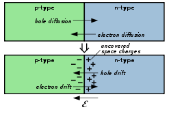
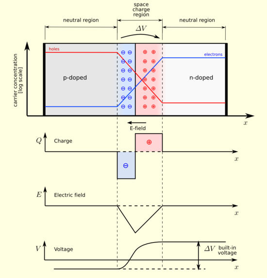 A depletion region forms instantaneously across a P-N junction
. It is most easily described when the junction is in thermal equilibrium or in a steady state
: in both of these cases the properties of the system do not vary in time; they have been called dynamic equilibrium
.
,
Electron
s and hole
s diffuse into regions with lower concentrations of electrons and holes, much as ink diffuses into water until it is uniformly distributed. By definition, N-type semiconductor has an excess of free electrons compared to the P-type region, and P-type has an excess of holes compared to the N-type region. Therefore when N-doped and P-doped pieces of semiconductor are placed together to form a junction, electrons migrate into the P-side and holes migrate into the N-side. Departure of an electron from the N-side to the P-side leaves a positive donor ion behind on the N-side, and likewise the hole leaves a negative acceptor ion on the P-side.
Following transfer, the diffused electrons come into contact with holes on the P-side and are eliminated by recombination. Likewise for the diffused holes on the N-side. The net result is the diffused electrons and holes are gone, leaving behind the charge
d ion
s adjacent to the interface in a region with no mobile carriers (called the depletion region). The uncompensated ions are positive on the N side and negative on the P side. This creates an electric field
that provides a force opposing the continued exchange of charge carriers. When the electric field is sufficient to arrest further transfer of holes and electrons, the depletion region has reached its equilibrium dimensions. Integrating the electric field across the depletion region determines what is called the built-in voltage (also called the junction voltage or barrier voltage or contact potential).
(1) Under reverse bias (P negative with respect to N), the potential drop (i.e., voltage) across the depletion region increases. This widens the depletion region, which increases the drift component of current and decreases the diffusion component. In this case the net current is leftward in the figure of the pn junction. The carrier density then is small and only a very small reverse saturation current flows.
(2) Forward bias (P positive with respect to N) narrows the depletion region and lowers the barrier to carrier injection. The diffusion component of the current greatly increases and the drift component decreases. In this case the net current is rightward in the figure of the pn junction. The carrier density is large (it varies exponentially with the applied bias voltage), making the junction conductive and allowing a large forward current. The mathematical description of the current is provided by the Shockley diode equation. The low current conducted under reverse bias and the large current under forward bias is an example of rectification
.
impurities. If a positive voltage now is applied to the gate, which is done by introducing positive charge Q to the gate, then some positively charged holes in the semiconductor nearest the gate are repelled by the positive charge on the gate, and exit the device through the bottom contact. They leave behind a depleted region that is insulating because no mobile holes remain; only the immobile, negatively charged acceptor impurities. The greater the positive charge placed on the gate, the more positive the applied gate voltage, and the more holes that leave the semiconductor surface, enlarging the depletion region. (In this device there is a limit to how wide the depletion width may become. It is set by the onset of an inversion layer of carriers in a thin layer, or channel, near the surface. The above discussion applies for positive voltages low enough that an inversion layer does not form.)
If the gate material is polysilicon of opposite type to the bulk semiconductor, then a spontaneous depletion region forms if the gate is electrically shorted to the substrate, in much the same manner as described for the pn-junction above.
 The principle of charge neutrality says the sum of positive charges must equal the sum of negative charges:
where n and p are the number of free electrons and holes, and and
and  are the number of ionized donors and acceptors, respectively. If we assume full ionization and that
  , then:
This condition ensures that the net negative acceptor charge exactly balances the net positive donor charge. The total depletion width in this case is the sum .
.
A full derivation for the depletion width is presented in reference. This derivation is based on solving the Poisson equation in one dimension – the dimension normal to the metallurgical junction. The electric field is zero outside of the depletion width (seen in above figure) and therefore Gauss’s law implies that the charge density in each region balance – as shown by the first equation in this sub-section. Treating each region separately and substituting the charge density for each region into the Poisson equation eventually leads to a result for the depletion width. This result for the depletion width is:

where is the semiconductor dielectric permitivity,
  is the built-in voltage, and
  is the applied bias. The depletion region is not symmetrically split between the n and p regions - it will tend towards the lightly doped side. A more complete analysis would take into account that there are still some carriers near the edges of the depletion region. This leads to an additional -2kT/q term in the last set of parentheses above.
 acceptors per unit volume, then charge neutrality requires the depletion width w to satisfy the relationship:
If the depletion width becomes wide enough, then electrons appear in a very thin layer at the semiconductor-oxide interface, called an inversion layer because they are oppositely charged to the holes that prevail in a P-type material. When an inversion layer forms the depletion width ceases to expand with increase in gate charge Q. In this case neutrality is achieved by attracting more electrons into the inversion layer. In the MOSFET this inversion layer is referred to as the channel.
. This occurs because the electric field in the depletion layer varies linearly in space from its (maximum) value at the gate to zero at the edge of the depletion width:
where A is the gate area, = 8.854×10⁻¹² F/m, F is the farad
and m is the meter. This linearly-varying electric field leads to an electrical potential that varies quadratically in space. The energy levels, or energy bands, bend in response to this potential.
Semiconductor
A semiconductor is a material with electrical conductivity due to electron flow intermediate in magnitude between that of a conductor and an insulator. This means a conductivity roughly in the range of 103 to 10−8 siemens per centimeter...
material where the mobile charge carrier
Charge carrier
In physics, a charge carrier is a free particle carrying an electric charge, especially the particles that carry electric currents in electrical conductors. Examples are electrons and ions...
s have diffused
Diffusion
Molecular diffusion, often called simply diffusion, is the thermal motion of all particles at temperatures above absolute zero. The rate of this movement is a function of temperature, viscosity of the fluid and the size of the particles...
away, or have been forced away by an electric field
Electric field
In physics, an electric field surrounds electrically charged particles and time-varying magnetic fields. The electric field depicts the force exerted on other electrically charged objects by the electrically charged particle the field is surrounding...
. The only elements left in the depletion region are ionized donor or acceptor impurities.
The 'depletion region' is so named because it is formed from a conducting region by removal of all free charge carriers, leaving none to carry a current. Understanding the depletion region is key to explaining modern semiconductor
Semiconductor
A semiconductor is a material with electrical conductivity due to electron flow intermediate in magnitude between that of a conductor and an insulator. This means a conductivity roughly in the range of 103 to 10−8 siemens per centimeter...
electronics
Electronics
Electronics is the branch of science, engineering and technology that deals with electrical circuits involving active electrical components such as vacuum tubes, transistors, diodes and integrated circuits, and associated passive interconnection technologies...
: diode
Diode
In electronics, a diode is a type of two-terminal electronic component with a nonlinear current–voltage characteristic. A semiconductor diode, the most common type today, is a crystalline piece of semiconductor material connected to two electrical terminals...
s, bipolar junction transistor
Bipolar junction transistor
|- align = "center"| || PNP|- align = "center"| || NPNA bipolar transistor is a three-terminal electronic device constructed of doped semiconductor material and may be used in amplifying or switching applications. Bipolar transistors are so named because their operation involves both electrons...
s, field-effect transistor
Field-effect transistor
The field-effect transistor is a transistor that relies on an electric field to control the shape and hence the conductivity of a channel of one type of charge carrier in a semiconductor material. FETs are sometimes called unipolar transistors to contrast their single-carrier-type operation with...
s, and variable capacitance diodes
Varicap
In electronics, a varicap diode, varactor diode, variable capacitance diode, variable reactance diode or tuning diode is a type of diode which has a variable capacitance that is a function of the voltage impressed on its terminals....
all rely on depletion region phenomena.
The following discussion is limited to the p-n junction
P-n junction
A p–n junction is formed at the boundary between a P-type and N-type semiconductor created in a single crystal of semiconductor by doping, for example by ion implantation, diffusion of dopants, or by epitaxy .If two separate pieces of material were used, this would...
and the MOS capacitor, but depletion regions arise in all the devices mentioned above.
Formation of depletion region in a P-N junction
P-n junction
A p–n junction is formed at the boundary between a P-type and N-type semiconductor created in a single crystal of semiconductor by doping, for example by ion implantation, diffusion of dopants, or by epitaxy .If two separate pieces of material were used, this would...
. It is most easily described when the junction is in thermal equilibrium or in a steady state
Steady state
A system in a steady state has numerous properties that are unchanging in time. This implies that for any property p of the system, the partial derivative with respect to time is zero:...
: in both of these cases the properties of the system do not vary in time; they have been called dynamic equilibrium
Dynamic equilibrium
A dynamic equilibrium exists once a reversible reaction ceases to change its ratio of reactants/products, but substances move between the chemicals at an equal rate, meaning there is no net change. It is a particular example of a system in a steady state...
.
,
Electron
Electron
The electron is a subatomic particle with a negative elementary electric charge. It has no known components or substructure; in other words, it is generally thought to be an elementary particle. An electron has a mass that is approximately 1/1836 that of the proton...
s and hole
Electron hole
An electron hole is the conceptual and mathematical opposite of an electron, useful in the study of physics, chemistry, and electrical engineering. The concept describes the lack of an electron at a position where one could exist in an atom or atomic lattice...
s diffuse into regions with lower concentrations of electrons and holes, much as ink diffuses into water until it is uniformly distributed. By definition, N-type semiconductor has an excess of free electrons compared to the P-type region, and P-type has an excess of holes compared to the N-type region. Therefore when N-doped and P-doped pieces of semiconductor are placed together to form a junction, electrons migrate into the P-side and holes migrate into the N-side. Departure of an electron from the N-side to the P-side leaves a positive donor ion behind on the N-side, and likewise the hole leaves a negative acceptor ion on the P-side.
Following transfer, the diffused electrons come into contact with holes on the P-side and are eliminated by recombination. Likewise for the diffused holes on the N-side. The net result is the diffused electrons and holes are gone, leaving behind the charge
Electric charge
Electric charge is a physical property of matter that causes it to experience a force when near other electrically charged matter. Electric charge comes in two types, called positive and negative. Two positively charged substances, or objects, experience a mutual repulsive force, as do two...
d ion
Ion
An ion is an atom or molecule in which the total number of electrons is not equal to the total number of protons, giving it a net positive or negative electrical charge. The name was given by physicist Michael Faraday for the substances that allow a current to pass between electrodes in a...
s adjacent to the interface in a region with no mobile carriers (called the depletion region). The uncompensated ions are positive on the N side and negative on the P side. This creates an electric field
Electric field
In physics, an electric field surrounds electrically charged particles and time-varying magnetic fields. The electric field depicts the force exerted on other electrically charged objects by the electrically charged particle the field is surrounding...
that provides a force opposing the continued exchange of charge carriers. When the electric field is sufficient to arrest further transfer of holes and electrons, the depletion region has reached its equilibrium dimensions. Integrating the electric field across the depletion region determines what is called the built-in voltage (also called the junction voltage or barrier voltage or contact potential).
- Mathematically speaking, charge transfer in semiconductor devices is due both to conduction driven by the electric field (drift) and by diffusion. For a P-type region, where holes conduct with electrical conductivity σ and diffuse with diffusion constant D, the net current density is given by
-
-
- jCurrent densityCurrent density is a measure of the density of flow of a conserved charge. Usually the charge is the electric charge, in which case the associated current density is the electric current per unit area of cross section, but the term current density can also be applied to other conserved...
= σ EElectric fieldIn physics, an electric field surrounds electrically charged particles and time-varying magnetic fields. The electric field depicts the force exerted on other electrically charged objects by the electrically charged particle the field is surrounding...
- D ∇qpCharge densityThe linear, surface, or volume charge density is the amount of electric charge in a line, surface, or volume, respectively. It is measured in coulombs per meter , square meter , or cubic meter , respectively, and represented by the lowercase Greek letter Rho . Since there are positive as well as...
- j
-
- with q the elementary chargeElementary chargeThe elementary charge, usually denoted as e, is the electric charge carried by a single proton, or equivalently, the absolute value of the electric charge carried by a single electron. This elementary charge is a fundamental physical constant. To avoid confusion over its sign, e is sometimes called...
(1.6×10⁻¹⁹ coulomb) and p the hole density (number per unit volume). Conduction forces the holes along the direction of the electric field. Diffusion moves the carriers in the direction of decreasing concentration, so for holes a negative current results for a positive density gradient. (If the carriers are electrons, we replace the hole density p by the negative of the electronElectron holeAn electron hole is the conceptual and mathematical opposite of an electron, useful in the study of physics, chemistry, and electrical engineering. The concept describes the lack of an electron at a position where one could exist in an atom or atomic lattice...
density n; in some cases, both electrons and holes must be included.) When the two current components balance, as in the pn-junction depletion region at dynamic equilibriumDynamic equilibriumA dynamic equilibrium exists once a reversible reaction ceases to change its ratio of reactants/products, but substances move between the chemicals at an equal rate, meaning there is no net change. It is a particular example of a system in a steady state...
, the current is zero due to the Einstein relation, which relates D to σ.
(1) Under reverse bias (P negative with respect to N), the potential drop (i.e., voltage) across the depletion region increases. This widens the depletion region, which increases the drift component of current and decreases the diffusion component. In this case the net current is leftward in the figure of the pn junction. The carrier density then is small and only a very small reverse saturation current flows.
(2) Forward bias (P positive with respect to N) narrows the depletion region and lowers the barrier to carrier injection. The diffusion component of the current greatly increases and the drift component decreases. In this case the net current is rightward in the figure of the pn junction. The carrier density is large (it varies exponentially with the applied bias voltage), making the junction conductive and allowing a large forward current. The mathematical description of the current is provided by the Shockley diode equation. The low current conducted under reverse bias and the large current under forward bias is an example of rectification
Rectifier
A rectifier is an electrical device that converts alternating current , which periodically reverses direction, to direct current , which flows in only one direction. The process is known as rectification...
.
Formation of depletion region in an MOS capacitor
Another example of a depletion region occurs in the MOS capacitor. It is shown in the figure to the right, for a P-type substrate. Suppose that the semiconductor initially is charge neutral, with the charge due to holes exactly balanced by the negative charge due to acceptor dopingExtrinsic semiconductor
An extrinsic semiconductor is a semiconductor that has been doped, that is, into which a doping agent has been introduced, giving it different electrical properties than the intrinsic semiconductor....
impurities. If a positive voltage now is applied to the gate, which is done by introducing positive charge Q to the gate, then some positively charged holes in the semiconductor nearest the gate are repelled by the positive charge on the gate, and exit the device through the bottom contact. They leave behind a depleted region that is insulating because no mobile holes remain; only the immobile, negatively charged acceptor impurities. The greater the positive charge placed on the gate, the more positive the applied gate voltage, and the more holes that leave the semiconductor surface, enlarging the depletion region. (In this device there is a limit to how wide the depletion width may become. It is set by the onset of an inversion layer of carriers in a thin layer, or channel, near the surface. The above discussion applies for positive voltages low enough that an inversion layer does not form.)
If the gate material is polysilicon of opposite type to the bulk semiconductor, then a spontaneous depletion region forms if the gate is electrically shorted to the substrate, in much the same manner as described for the pn-junction above.
Depletion width
Depletion width describes the width of the depletion region in a semiconductor, particularly in geometries that are one-dimensional, like the pn-junction and MOS capacitor. The width of the depletion region is governed by the principle of charge neutrality. Two examples follow:Depletion width in pn-junction
-
-
 ,
,
-
where n and p are the number of free electrons and holes, and
and are the number of ionized donors and acceptors, respectively. If we assume full ionization and that , then:-
-
 .
.
-
This condition ensures that the net negative acceptor charge exactly balances the net positive donor charge. The total depletion width in this case is the sum
.A full derivation for the depletion width is presented in reference. This derivation is based on solving the Poisson equation in one dimension – the dimension normal to the metallurgical junction. The electric field is zero outside of the depletion width (seen in above figure) and therefore Gauss’s law implies that the charge density in each region balance – as shown by the first equation in this sub-section. Treating each region separately and substituting the charge density for each region into the Poisson equation eventually leads to a result for the depletion width. This result for the depletion width is:
where
is the semiconductor dielectric permitivity, is the built-in voltage, and is the applied bias. The depletion region is not symmetrically split between the n and p regions - it will tend towards the lightly doped side. A more complete analysis would take into account that there are still some carriers near the edges of the depletion region. This leads to an additional -2kT/q term in the last set of parentheses above.Depletion width in MOS capacitor
Again, the governing principle is charge neutrality. Let us assume a P-type substrate. If positive charge Q is placed on the gate, then holes are depleted to a depth w sufficient to expose sufficient negative acceptors to exactly balance the gate charge. Supposing the dopant density to be acceptors per unit volume, then charge neutrality requires the depletion width w to satisfy the relationship:
If the depletion width becomes wide enough, then electrons appear in a very thin layer at the semiconductor-oxide interface, called an inversion layer because they are oppositely charged to the holes that prevail in a P-type material. When an inversion layer forms the depletion width ceases to expand with increase in gate charge Q. In this case neutrality is achieved by attracting more electrons into the inversion layer. In the MOSFET this inversion layer is referred to as the channel.
Electric field in depletion layer and band bending
Associated with the depletion layer is an effect known as band bendingBand bending
Band bending refers to the local change in energy of electrons at a semiconductor junction due to space charge effects. Because the common way to visualize the electron energy states and Fermi level in a material is to draw bands on an energy vs...
. This occurs because the electric field in the depletion layer varies linearly in space from its (maximum) value
at the gate to zero at the edge of the depletion width:
where A is the gate area,
= 8.854×10⁻¹² F/m, F is the faradFarad
The farad is the SI unit of capacitance. The unit is named after the English physicist Michael Faraday.- Definition :A farad is the charge in coulombs which a capacitor will accept for the potential across it to change 1 volt. A coulomb is 1 ampere second...
and m is the meter. This linearly-varying electric field leads to an electrical potential that varies quadratically in space. The energy levels, or energy bands, bend in response to this potential.
See also
- Capacitance voltage profiling
- Metal–oxide–semiconductor structure
- Semiconductor diodes