
Bipolar junction transistor
Encyclopedia
|- align = "center"
|.svg.png) || PNP
|| PNP
|- align = "center"
|.svg.png) || NPN
|| NPN
A bipolar (junction) transistor
(BJT) is a three-terminal electronic device constructed of doped semiconductor
material and may be used in amplifying
or switching applications. Bipolar transistors are so named because their operation involves both electron
s and hole
s. Charge flow in a BJT is due to bidirectional diffusion
of charge carriers
across a junction between two regions of different charge concentrations. This mode of operation is contrasted with unipolar transistors, such as field-effect transistor
s, in which only one carrier type is involved in charge flow due to drift
. By design, most of the BJT collector current is due to the flow of charges injected from a high-concentration emitter into the base where they are minority carriers that diffuse toward the collector, and so BJTs are classified as minority-carrier devices.
.svg.png) An NPN transistor can be considered as two diode
An NPN transistor can be considered as two diode
s with a shared anode
. In typical operation, the base-emitter junction
is forward biased and the base–collector junction is reverse biased. In an NPN transistor, for example, when a positive voltage is applied to the base–emitter junction, the equilibrium between thermally generated carrier
s and the repelling electric field of the depletion region
becomes unbalanced, allowing thermally excited electrons to inject into the base region. These electrons wander (or "diffuse
") through the base from the region of high concentration near the emitter towards the region of low concentration near the collector. The electrons in the base are called minority carriers because the base is doped p-type which would make holes the majority carrier in the base.
To minimize the percentage of carriers that recombine
before reaching the collector–base junction, the transistor's base region must be thin enough that carriers can diffuse across it in much less time than the semiconductor's minority carrier lifetime. In particular, the thickness of the base must be much less than the diffusion length of the electrons. The collector–base junction is reverse-biased, and so little electron injection occurs from the collector to the base, but electrons that diffuse through the base towards the collector are swept into the collector by the electric field in the depletion region of the collector–base junction. The thin shared base and asymmetric collector–emitter doping is what differentiates a bipolar transistor from two separate and oppositely biased diodes connected in series.
(diode).
The physical explanation for collector current is the amount of minority-carrier charge in the base region. Detailed models of transistor action, such as the Gummel–Poon model
, account for the distribution of this charge explicitly to explain transistor behavior more exactly. The charge-control view easily handles phototransistors, where minority carriers in the base region are created by the absorption of photon
s, and handles the dynamics of turn-off, or recovery time, which depends on charge in the base region recombining. However, because base charge is not a signal that is visible at the terminals, the current- and voltage-control views are generally used in circuit design and analysis.
In analog circuit design, the current-control view is sometimes used because it is approximately linear. That is, the collector current is approximately times the base current. Some basic circuits can be designed by assuming that the emitter–base voltage is approximately constant, and that collector current is beta times the base current. However, to accurately and reliably design production BJT circuits, the voltage-control (for example, Ebers–Moll) model is required. The voltage-control model requires an exponential function to be taken into account, but when it is linearized such that the transistor can be modelled as a transconductance, as in the Ebers–Moll model, design for circuits such as differential amplifiers again becomes a mostly linear problem, so the voltage-control view is often preferred. For translinear circuit
s, in which the exponential I–V curve is key to the operation, the transistors are usually modelled as voltage controlled with transconductance
proportional to collector current. In general, transistor level circuit design is performed using SPICE
or a comparable analog circuit simulator, so model complexity is usually not of much concern to the designer.
.
Alpha and beta are more precisely related by the following identities (NPN transistor):
semiconductor regions, the emitter region, the base region and the collector region. These regions are, respectively, p type, n type and p type in a PNP, and n type, p type and n type in a NPN transistor. Each semiconductor region is connected to a terminal, appropriately labeled: emitter (E), base (B) and collector (C).
The base is physically located between the emitter and the collector and is made from lightly doped, high resistivity material. The collector surrounds the emitter region, making it almost impossible for the electrons injected into the base region to escape being collected, thus making the resulting value of α very close to unity, and so, giving the transistor a large β. A cross section view of a BJT indicates that the collector–base junction has a much larger area than the emitter–base junction.
The bipolar junction transistor, unlike other transistors, is usually not a symmetrical device. This means that interchanging the collector and the emitter makes the transistor leave the forward active mode and start to operate in reverse mode. Because the transistor's internal structure is usually optimized for forward-mode operation, interchanging the collector and the emitter makes the values of α and β in reverse operation much smaller than those in forward operation; often the α of the reverse mode is lower than 0.5. The lack of symmetry is primarily due to the doping ratios of the emitter and the collector. The emitter is heavily doped, while the collector is lightly doped, allowing a large reverse bias voltage to be applied before the collector–base junction breaks down. The collector–base junction is reverse biased in normal operation. The reason the emitter is heavily doped is to increase the emitter injection efficiency: the ratio of carriers injected by the emitter to those injected by the base. For high current gain, most of the carriers injected into the emitter–base junction must come from the emitter.
 The low-performance "lateral" bipolar transistors sometimes used in CMOS
processes are sometimes designed symmetrically, that is, with no difference between forward and backward operation.
Small changes in the voltage applied across the base–emitter terminals causes the current that flows between the emitter and the collector to change significantly. This effect can be used to amplify the input voltage or current. BJTs can be thought of as voltage-controlled current source
s, but are more simply characterized as current-controlled current sources, or current amplifiers, due to the low impedance at the base.
Early transistors were made from germanium
but most modern BJTs are made from silicon
. A significant minority are also now made from gallium arsenide, especially for very high speed applications (see HBT, below).
Most of the NPN current is carried by electrons, moving from emitter to collector as minority carriers in the P-type base region. Most bipolar transistors used today are NPN, because electron mobility
is higher than hole mobility in semiconductors, allowing greater currents and faster operation.
A mnemonic
device for the remembering the symbol for an NPN transistor is not pointing in, based on the arrows in the symbol and the letters in the name. That is, the NPN transistor is the BJT transistor that is "not pointing in".
The arrows in the NPN and PNP transistor symbols are on the emitter legs and point in the direction of the conventional current flow when the device is in forward active mode.
A mnemonic device for the remembering the symbol for a PNP transistor is pointing in (proudly), based on the arrows in the symbol and the letters in the name. That is, the PNP transistor is the BJT transistor that is "pointing in".
(HBT) is an improvement of the BJT that can handle signals of very high frequencies up to several hundred GHz
. It is common in modern ultrafast circuits, mostly RF
systems.
Heterojunction transistors have different semiconductors for the elements of the transistor. Usually the emitter is composed of a larger bandgap material than the base. The figure shows that this difference in bandgap allows the barrier for holes to inject backward into the base, denoted in figure as Δφp, to be made large, while the barrier for electrons to inject into the base Δφn is made low. This barrier arrangement helps reduce minority carrier injection from the base when the emitter-base junction is under forward bias, and thus reduces base current and increases emitter injection efficiency.
The improved injection of carriers into the base allows the base to have a higher doping level, resulting in lower resistance to access the base electrode. In the more traditional BJT, also referred to as homojunction BJT, the efficiency of carrier injection from the emitter to the base is primarily determined by the doping ratio between the emitter and base, which means the base must be lightly doped to obtain high injection efficiency, making its resistance relatively high. In addition, higher doping in the base can improve figures of merit like the Early voltage by lessening base narrowing.
The grading of composition in the base, for example, by progressively increasing the amount of germanium in a SiGe
transistor, causes a gradient in bandgap in the neutral base, denoted in the figure by ΔφG, providing a "built-in" field that assists electron transport across the base. That drift component of transport aids the normal diffusive transport, increasing the frequency response of the transistor by shortening the transit time across the base.
Two commonly used HBTs are silicon–germanium and aluminum gallium arsenide, though a wide variety of semiconductors may be used for the HBT structure. HBT structures are usually grown by epitaxy
techniques like MOCVD
and MBE
.
Bias (NPN) !! Mode (NPN)
|-
|E < B < C || Forward || Reverse || Forward active
|-
|E < B > C || Forward || Forward || Saturation
|-
|E > B < C || Reverse || Reverse || Cut-off
|-
|E > B > C || Reverse || Forward || Reverse-active
|-
!Applied voltages!!B-E Junction
Bias (PNP)!!B-C Junction
Bias (PNP)!!Mode (PNP)
|-
|E < B < C || Reverse || Forward || Reverse-active
|-
|E < B > C || Reverse || Reverse || Cut-off
|-
|E > B < C || Forward || Forward || Saturation
|-
|E > B > C || Forward || Reverse || Forward active
|}
|
|| PNP|- align = "center"
|
|| NPNA bipolar (junction) transistor
Transistor
A transistor is a semiconductor device used to amplify and switch electronic signals and power. It is composed of a semiconductor material with at least three terminals for connection to an external circuit. A voltage or current applied to one pair of the transistor's terminals changes the current...
(BJT) is a three-terminal electronic device constructed of doped semiconductor
Semiconductor
A semiconductor is a material with electrical conductivity due to electron flow intermediate in magnitude between that of a conductor and an insulator. This means a conductivity roughly in the range of 103 to 10−8 siemens per centimeter...
material and may be used in amplifying
Electronic amplifier
An electronic amplifier is a device for increasing the power of a signal.It does this by taking energy from a power supply and controlling the output to match the input signal shape but with a larger amplitude...
or switching applications. Bipolar transistors are so named because their operation involves both electron
Electron
The electron is a subatomic particle with a negative elementary electric charge. It has no known components or substructure; in other words, it is generally thought to be an elementary particle. An electron has a mass that is approximately 1/1836 that of the proton...
s and hole
Electron hole
An electron hole is the conceptual and mathematical opposite of an electron, useful in the study of physics, chemistry, and electrical engineering. The concept describes the lack of an electron at a position where one could exist in an atom or atomic lattice...
s. Charge flow in a BJT is due to bidirectional diffusion
Diffusion
Molecular diffusion, often called simply diffusion, is the thermal motion of all particles at temperatures above absolute zero. The rate of this movement is a function of temperature, viscosity of the fluid and the size of the particles...
of charge carriers
Charge carriers in semiconductors
There are two recognized types of charge carriers in semiconductors. One of them is electrons, which carry negative electric charge. In addition, it is convenient to treat the traveling vacancies in the valence-band electron population as the second type of charge carriers, which carry a positive...
across a junction between two regions of different charge concentrations. This mode of operation is contrasted with unipolar transistors, such as field-effect transistor
Field-effect transistor
The field-effect transistor is a transistor that relies on an electric field to control the shape and hence the conductivity of a channel of one type of charge carrier in a semiconductor material. FETs are sometimes called unipolar transistors to contrast their single-carrier-type operation with...
s, in which only one carrier type is involved in charge flow due to drift
Drift velocity
The drift velocity is the average velocity that a particle, such as an electron, attains due to an electric field. It can also be referred to as Axial Drift Velocity since particles defined are assumed to be moving along a plane. In general, an electron will 'rattle around' in a conductor at the...
. By design, most of the BJT collector current is due to the flow of charges injected from a high-concentration emitter into the base where they are minority carriers that diffuse toward the collector, and so BJTs are classified as minority-carrier devices.
Introduction
Diode
In electronics, a diode is a type of two-terminal electronic component with a nonlinear current–voltage characteristic. A semiconductor diode, the most common type today, is a crystalline piece of semiconductor material connected to two electrical terminals...
s with a shared anode
Anode
An anode is an electrode through which electric current flows into a polarized electrical device. Mnemonic: ACID ....
. In typical operation, the base-emitter junction
P-n junction
A p–n junction is formed at the boundary between a P-type and N-type semiconductor created in a single crystal of semiconductor by doping, for example by ion implantation, diffusion of dopants, or by epitaxy .If two separate pieces of material were used, this would...
is forward biased and the base–collector junction is reverse biased. In an NPN transistor, for example, when a positive voltage is applied to the base–emitter junction, the equilibrium between thermally generated carrier
Charge carrier
In physics, a charge carrier is a free particle carrying an electric charge, especially the particles that carry electric currents in electrical conductors. Examples are electrons and ions...
s and the repelling electric field of the depletion region
Depletion region
In semiconductor physics, the depletion region, also called depletion layer, depletion zone, junction region or the space charge region, is an insulating region within a conductive, doped semiconductor material where the mobile charge carriers have diffused away, or have been forced away by an...
becomes unbalanced, allowing thermally excited electrons to inject into the base region. These electrons wander (or "diffuse
Diffusion
Molecular diffusion, often called simply diffusion, is the thermal motion of all particles at temperatures above absolute zero. The rate of this movement is a function of temperature, viscosity of the fluid and the size of the particles...
") through the base from the region of high concentration near the emitter towards the region of low concentration near the collector. The electrons in the base are called minority carriers because the base is doped p-type which would make holes the majority carrier in the base.
To minimize the percentage of carriers that recombine
Carrier generation and recombination
In the solid state physics of semiconductors, carrier generation and recombination are processes by which mobile charge carriers are created and eliminated. Carrier generation and recombination processes are fundamental to the operation of many optoelectronic semiconductor devices, such as...
before reaching the collector–base junction, the transistor's base region must be thin enough that carriers can diffuse across it in much less time than the semiconductor's minority carrier lifetime. In particular, the thickness of the base must be much less than the diffusion length of the electrons. The collector–base junction is reverse-biased, and so little electron injection occurs from the collector to the base, but electrons that diffuse through the base towards the collector are swept into the collector by the electric field in the depletion region of the collector–base junction. The thin shared base and asymmetric collector–emitter doping is what differentiates a bipolar transistor from two separate and oppositely biased diodes connected in series.
Voltage, current, and charge control
The collector–emitter current can be viewed as being controlled by the base–emitter current (current control), or by the base–emitter voltage (voltage control). These views are related by the current–voltage relation of the base–emitter junction, which is just the usual exponential current–voltage curve of a p-n junctionP-n junction
A p–n junction is formed at the boundary between a P-type and N-type semiconductor created in a single crystal of semiconductor by doping, for example by ion implantation, diffusion of dopants, or by epitaxy .If two separate pieces of material were used, this would...
(diode).
The physical explanation for collector current is the amount of minority-carrier charge in the base region. Detailed models of transistor action, such as the Gummel–Poon model
Gummel–Poon model
The Gummel–Poon model is a model of the bipolar junction transistor. It was first described in a paper published by Hermann Gummel and H. C. Poon at Bell Labs in 1970....
, account for the distribution of this charge explicitly to explain transistor behavior more exactly. The charge-control view easily handles phototransistors, where minority carriers in the base region are created by the absorption of photon
Photon
In physics, a photon is an elementary particle, the quantum of the electromagnetic interaction and the basic unit of light and all other forms of electromagnetic radiation. It is also the force carrier for the electromagnetic force...
s, and handles the dynamics of turn-off, or recovery time, which depends on charge in the base region recombining. However, because base charge is not a signal that is visible at the terminals, the current- and voltage-control views are generally used in circuit design and analysis.
In analog circuit design, the current-control view is sometimes used because it is approximately linear. That is, the collector current is approximately
times the base current. Some basic circuits can be designed by assuming that the emitter–base voltage is approximately constant, and that collector current is beta times the base current. However, to accurately and reliably design production BJT circuits, the voltage-control (for example, Ebers–Moll) model is required. The voltage-control model requires an exponential function to be taken into account, but when it is linearized such that the transistor can be modelled as a transconductance, as in the Ebers–Moll model, design for circuits such as differential amplifiers again becomes a mostly linear problem, so the voltage-control view is often preferred. For translinear circuitTranslinear circuit
A translinear circuit is a circuit that carries out its function using the translinear principle. These are current-mode circuits that can be made using transistors that obey an exponential current-voltage characteristic—this includes BJTs and CMOS transistors in weak inversion.The word translinear...
s, in which the exponential I–V curve is key to the operation, the transistors are usually modelled as voltage controlled with transconductance
Transconductance
Transconductance, also known as mutual conductance, is a property of certain electronic components. Conductance is the reciprocal of resistance; transconductance, meanwhile, is the ratio of the current change at the output port to the voltage change at the input port. It is written as gm...
proportional to collector current. In general, transistor level circuit design is performed using SPICE
SPICE
SPICE is a general-purpose, open source analog electronic circuit simulator.It is a powerful program that is used in integrated circuit and board-level design to check the integrity of circuit designs and to predict circuit behavior.- Introduction :Unlike board-level designs composed of discrete...
or a comparable analog circuit simulator, so model complexity is usually not of much concern to the designer.
Turn-on, turn-off, and storage delay
The Bipolar transistor exhibits a few delay characteristics when turning on and off. Most transistors, and especially power transistors, exhibit long base-storage times that limit maximum frequency of operation in switching applications. One method for reducing this storage time is by using a Baker clampBaker clamp
Baker clamp is a generic name for a class of electronic circuits that reduce the storage time of a switching bipolar junction transistor by applying a nonlinear negative feedback through various kinds of diodes. The reason for slow turn-off times of saturated BJTs is the stored charge in the base...
.
Transistor 'alpha' and 'beta'
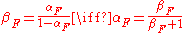
The proportion of electrons able to cross the base and reach the collector is a measure of the BJT efficiency. The heavy doping of the emitter region and light doping of the base region causes many more electrons to be injected from the emitter into the base than holes to be injected from the base into the emitter. The common-emitter current gain is represented by βF or hFE; it is approximately the ratio of the DC collector current to the DC base current in forward-active region. It is typically greater than 100 for small-signal transistors but can be smaller in transistors designed for high-power applications. Another important parameter is the common-base current gain, αF. The common-base current gain is approximately the gain of current from emitter to collector in the forward-active region. This ratio usually has a value close to unity; between 0.98 and 0.998.Alpha and beta are more precisely related by the following identities (NPN transistor):


Structure
A BJT consists of three differently dopedDoping (semiconductor)
In semiconductor production, doping intentionally introduces impurities into an extremely pure semiconductor for the purpose of modulating its electrical properties. The impurities are dependent upon the type of semiconductor. Lightly and moderately doped semiconductors are referred to as extrinsic...
semiconductor regions, the emitter region, the base region and the collector region. These regions are, respectively, p type, n type and p type in a PNP, and n type, p type and n type in a NPN transistor. Each semiconductor region is connected to a terminal, appropriately labeled: emitter (E), base (B) and collector (C).
The base is physically located between the emitter and the collector and is made from lightly doped, high resistivity material. The collector surrounds the emitter region, making it almost impossible for the electrons injected into the base region to escape being collected, thus making the resulting value of α very close to unity, and so, giving the transistor a large β. A cross section view of a BJT indicates that the collector–base junction has a much larger area than the emitter–base junction.
The bipolar junction transistor, unlike other transistors, is usually not a symmetrical device. This means that interchanging the collector and the emitter makes the transistor leave the forward active mode and start to operate in reverse mode. Because the transistor's internal structure is usually optimized for forward-mode operation, interchanging the collector and the emitter makes the values of α and β in reverse operation much smaller than those in forward operation; often the α of the reverse mode is lower than 0.5. The lack of symmetry is primarily due to the doping ratios of the emitter and the collector. The emitter is heavily doped, while the collector is lightly doped, allowing a large reverse bias voltage to be applied before the collector–base junction breaks down. The collector–base junction is reverse biased in normal operation. The reason the emitter is heavily doped is to increase the emitter injection efficiency: the ratio of carriers injected by the emitter to those injected by the base. For high current gain, most of the carriers injected into the emitter–base junction must come from the emitter.
CMOS
Complementary metal–oxide–semiconductor is a technology for constructing integrated circuits. CMOS technology is used in microprocessors, microcontrollers, static RAM, and other digital logic circuits...
processes are sometimes designed symmetrically, that is, with no difference between forward and backward operation.
Small changes in the voltage applied across the base–emitter terminals causes the current that flows between the emitter and the collector to change significantly. This effect can be used to amplify the input voltage or current. BJTs can be thought of as voltage-controlled current source
Current source
A current source is an electrical or electronic device that delivers or absorbs electric current. A current source is the dual of a voltage source. The term constant-current sink is sometimes used for sources fed from a negative voltage supply...
s, but are more simply characterized as current-controlled current sources, or current amplifiers, due to the low impedance at the base.
Early transistors were made from germanium
Germanium
Germanium is a chemical element with the symbol Ge and atomic number 32. It is a lustrous, hard, grayish-white metalloid in the carbon group, chemically similar to its group neighbors tin and silicon. The isolated element is a semiconductor, with an appearance most similar to elemental silicon....
but most modern BJTs are made from silicon
Silicon
Silicon is a chemical element with the symbol Si and atomic number 14. A tetravalent metalloid, it is less reactive than its chemical analog carbon, the nonmetal directly above it in the periodic table, but more reactive than germanium, the metalloid directly below it in the table...
. A significant minority are also now made from gallium arsenide, especially for very high speed applications (see HBT, below).
NPN
NPN is one of the two types of bipolar transistors, consisting of a layer of P-doped semiconductor (the "base") between two N-doped layers. A small current entering the base is amplified to produce a large collector and emitter current. That is, an NPN transistor is "on" when its base is pulled high relative to the emitter.Most of the NPN current is carried by electrons, moving from emitter to collector as minority carriers in the P-type base region. Most bipolar transistors used today are NPN, because electron mobility
Electron mobility
In solid-state physics, the electron mobility characterizes how quickly an electron can move through a metal or semiconductor, when pulled by an electric field. In semiconductors, there is an analogous quantity for holes, called hole mobility...
is higher than hole mobility in semiconductors, allowing greater currents and faster operation.
A mnemonic
Mnemonic
A mnemonic , or mnemonic device, is any learning technique that aids memory. To improve long term memory, mnemonic systems are used to make memorization easier. Commonly encountered mnemonics are often verbal, such as a very short poem or a special word used to help a person remember something,...
device for the remembering the symbol for an NPN transistor is not pointing in, based on the arrows in the symbol and the letters in the name. That is, the NPN transistor is the BJT transistor that is "not pointing in".
PNP
The other type of BJT is the PNP, consisting of a layer of N-doped semiconductor between two layers of P-doped material. A small current leaving the base is amplified in the collector output. That is, a PNP transistor is "on" when its base is pulled low relative to the emitter.The arrows in the NPN and PNP transistor symbols are on the emitter legs and point in the direction of the conventional current flow when the device is in forward active mode.
A mnemonic device for the remembering the symbol for a PNP transistor is pointing in (proudly), based on the arrows in the symbol and the letters in the name. That is, the PNP transistor is the BJT transistor that is "pointing in".
Heterojunction bipolar transistor
The heterojunction bipolar transistorHeterojunction bipolar transistor
The heterojunction bipolar transistor is a type of bipolar junction transistor which uses differing semiconductor materials for the emitter and base regions, creating a heterojunction. The HBT improves on the BJT in that it that can handle signals of very high frequencies, up to several hundred...
(HBT) is an improvement of the BJT that can handle signals of very high frequencies up to several hundred GHz
Hertz
The hertz is the SI unit of frequency defined as the number of cycles per second of a periodic phenomenon. One of its most common uses is the description of the sine wave, particularly those used in radio and audio applications....
. It is common in modern ultrafast circuits, mostly RF
Radio frequency
Radio frequency is a rate of oscillation in the range of about 3 kHz to 300 GHz, which corresponds to the frequency of radio waves, and the alternating currents which carry radio signals...
systems.
Heterojunction transistors have different semiconductors for the elements of the transistor. Usually the emitter is composed of a larger bandgap material than the base. The figure shows that this difference in bandgap allows the barrier for holes to inject backward into the base, denoted in figure as Δφp, to be made large, while the barrier for electrons to inject into the base Δφn is made low. This barrier arrangement helps reduce minority carrier injection from the base when the emitter-base junction is under forward bias, and thus reduces base current and increases emitter injection efficiency.
The improved injection of carriers into the base allows the base to have a higher doping level, resulting in lower resistance to access the base electrode. In the more traditional BJT, also referred to as homojunction BJT, the efficiency of carrier injection from the emitter to the base is primarily determined by the doping ratio between the emitter and base, which means the base must be lightly doped to obtain high injection efficiency, making its resistance relatively high. In addition, higher doping in the base can improve figures of merit like the Early voltage by lessening base narrowing.
The grading of composition in the base, for example, by progressively increasing the amount of germanium in a SiGe
SiGe
SiGe , or silicon-germanium, is a general term for the alloy Si1−xGex which consists of any molar ratio of silicon and germanium. It is commonly used as a semiconductor material in integrated circuits for heterojunction bipolar transistors or as a strain-inducing layer for CMOS transistors...
transistor, causes a gradient in bandgap in the neutral base, denoted in the figure by ΔφG, providing a "built-in" field that assists electron transport across the base. That drift component of transport aids the normal diffusive transport, increasing the frequency response of the transistor by shortening the transit time across the base.
Two commonly used HBTs are silicon–germanium and aluminum gallium arsenide, though a wide variety of semiconductors may be used for the HBT structure. HBT structures are usually grown by epitaxy
Epitaxy
Epitaxy refers to the deposition of a crystalline overlayer on a crystalline substrate, where the overlayer is in registry with the substrate. In other words, there must be one or more preferred orientations of the overlayer with respect to the substrate for this to be termed epitaxial growth. The...
techniques like MOCVD
Metalorganic vapour phase epitaxy
Metalorganic vapour phase epitaxy , also known as organometallic vapour phase epitaxy or metalorganic chemical vapour deposition , is a chemical vapour deposition method of epitaxial growth of materials, especially compound semiconductors, from the surface reaction of organic compounds or...
and MBE
Molecular beam epitaxy
Molecular beam epitaxy is one of several methods of depositing single crystals. It was invented in the late 1960s at Bell Telephone Laboratories by J. R. Arthur and Alfred Y. Cho.-Method:...
.
Regions of operation
Bias (NPN)!!B-C JunctionBias (NPN) !! Mode (NPN)
|-
|E < B < C || Forward || Reverse || Forward active
|-
|E < B > C || Forward || Forward || Saturation
|-
|E > B < C || Reverse || Reverse || Cut-off
|-
|E > B > C || Reverse || Forward || Reverse-active
|-
!Applied voltages!!B-E Junction
Bias (PNP)!!B-C Junction
Bias (PNP)!!Mode (PNP)
|-
|E < B < C || Reverse || Forward || Reverse-active
|-
|E < B > C || Reverse || Reverse || Cut-off
|-
|E > B < C || Forward || Forward || Saturation
|-
|E > B > C || Forward || Reverse || Forward active
|}
Bipolar transistors have five distinct regions of operation, defined by BJT junction biases.
The modes of operation can be described in terms of the applied voltages (this description applies to NPN transistors; polarities are reversed for PNP transistors):
- Forward active: base higher than emitter, collector higher than base (in this mode the collector current is proportional to base current by
 ).
). - Saturation: base higher than emitter, but collector is not higher than base.
- Cut-Off: base lower than emitter, but collector is higher than base. It means the transistor is not letting conventional current to go through collector to emitter.
- Reverse-active: base lower than emitter, collector lower than base: reverse conventional current goes through transistor.
In terms of junction biasing:
('reverse biased base–collector junction' means Vbc < 0 for NPN, opposite for PNP)
- Forward-active (or simply, active): The base–emitter junction is forward biased and the base–collector junction is reverse biased. Most bipolar transistors are designed to afford the greatest common-emitter current gain, βF, in forward-active mode. If this is the case, the collector–emitter current is approximately proportionalProportionality (mathematics)In mathematics, two variable quantities are proportional if one of them is always the product of the other and a constant quantity, called the coefficient of proportionality or proportionality constant. In other words, are proportional if the ratio \tfrac yx is constant. We also say that one...
to the base current, but many times larger, for small base current variations. - Reverse-active (or inverse-active or inverted): By reversing the biasing conditions of the forward-active region, a bipolar transistor goes into reverse-active mode. In this mode, the emitter and collector regions switch roles. Because most BJTs are designed to maximize current gain in forward-active mode, the βF in inverted mode is several (2–3 for the ordinary germanium transistor) times smaller. This transistor mode is seldom used, usually being considered only for failsafe conditions and some types of bipolar logic. The reverse bias breakdown voltage to the base may be an order of magnitude lower in this region.
- Saturation: With both junctions forward-biased, a BJT is in saturation mode and facilitates high current conduction from the emitter to the collector (or the other direction in the case of NPN, with negatively charged carriers flowing from emitter to collector). This mode corresponds to a logical "on", or a closed switch.
- Cutoff: In cutoff, biasing conditions opposite of saturation (both junctions reverse biased) are present. There is very little current, which corresponds to a logical "off", or an open switch.
- Avalanche breakdownAvalanche breakdownAvalanche breakdown is a phenomenon that can occur in both insulating and semiconducting materials. It is a form of electric current multiplication that can allow very large currents within materials which are otherwise good insulators. It is a type of electron avalanche...
region
Although these regions are well defined for sufficiently large applied voltage, they overlap somewhat for small (less than a few hundred millivolts) biases. For example, in the typical grounded-emitter configuration of an NPN BJT used as a pulldown switch in digital logic, the "off" state never involves a reverse-biased junction because the base voltage never goes below ground; nevertheless the forward bias is close enough to zero that essentially no current flows, so this end of the forward active region can be regarded as the cutoff region.
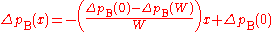
Active-mode NPN transistors in circuits
The diagram opposite is a schematic representation of an NPN transistor connected to two voltage sources. To make the transistor conduct appreciable current (on the order of 1 mA) from C to E, VBE must be above a minimum value sometimes referred to as the cut-in voltage. The cut-in voltage is usually about 600 mV for silicon BJTs at room temperatureRoom temperature
-Comfort levels:The American Society of Heating, Refrigerating and Air-Conditioning Engineers has listings for suggested temperatures and air flow rates in different types of buildings and different environmental circumstances. For example, a single office in a building has an occupancy ratio per...
but can be different depending on the type of transistor and its biasing
Biasing (electronics)
Biasing in electronics is the method of establishing predetermined voltages and/or currents at various points of an electronic circuit to set an appropriate operating point...
. This applied voltage causes the lower P-N junction to 'turn-on' allowing a flow of electrons from the emitter into the base. In active mode, the electric field existing between base and collector (caused by VCE) will cause the majority of these electrons to cross the upper P-N junction into the collector to form the collector current IC. The remainder of the electrons recombine with holes, the majority carriers in the base, making a current through the base connection to form the base current, IB. As shown in the diagram, the emitter current, IE, is the total transistor current, which is the sum of the other terminal currents, (i.e., IE = IB + IC).
In the diagram, the arrows representing current point in the direction of conventional current – the flow of electrons is in the opposite direction of the arrows because electrons carry negative electric charge
Electric charge
Electric charge is a physical property of matter that causes it to experience a force when near other electrically charged matter. Electric charge comes in two types, called positive and negative. Two positively charged substances, or objects, experience a mutual repulsive force, as do two...
. In active mode, the ratio of the collector current to the base current is called the DC current gain. This gain is usually 100 or more, but robust circuit designs do not depend on the exact value (for example see op-amp). The value of this gain for DC signals is referred to as
 , and the value of this gain for AC signals is referred to as
  . However, when there is no particular frequency range of interest, the symbol
  is used.
It should also be noted that the emitter current is related to
 exponentially. At room temperature
Room temperature
-Comfort levels:The American Society of Heating, Refrigerating and Air-Conditioning Engineers has listings for suggested temperatures and air flow rates in different types of buildings and different environmental circumstances. For example, a single office in a building has an occupancy ratio per...
, an increase in
 by approximately 60 mV increases the emitter current by a factor of 10. Because the base current is approximately proportional to the collector and emitter currents, they vary in the same way.
Active-mode PNP transistors in circuits
The diagram opposite is a schematic representation of a PNP transistor connected to two voltage sources. To make the transistor conduct appreciable current (on the order of 1 mA) from E to C, must be above a minimum value sometimes referred to as the cut-in voltage. The cut-in voltage is usually about 600 mV for silicon BJTs at room temperature
Room temperature
-Comfort levels:The American Society of Heating, Refrigerating and Air-Conditioning Engineers has listings for suggested temperatures and air flow rates in different types of buildings and different environmental circumstances. For example, a single office in a building has an occupancy ratio per...
but can be different depending on the type of transistor and its biasing
Biasing (electronics)
Biasing in electronics is the method of establishing predetermined voltages and/or currents at various points of an electronic circuit to set an appropriate operating point...
. This applied voltage causes the upper P-N junction to 'turn-on' allowing a flow of holes
Electron hole
An electron hole is the conceptual and mathematical opposite of an electron, useful in the study of physics, chemistry, and electrical engineering. The concept describes the lack of an electron at a position where one could exist in an atom or atomic lattice...
from the emitter into the base. In active mode, the electric field existing between the emitter and the collector (caused by
 ) causes the majority of these holes to cross the lower P-N junction into the collector to form the collector current
  . The remainder of the holes recombine with electrons, the majority carriers in the base, making a current through the base connection to form the base current,
  . As shown in the diagram, the emitter current,
  , is the total transistor current, which is the sum of the other terminal currents (i.e., IE = IB + IC).
In the diagram, the arrows representing current point in the direction of conventional current – the flow of holes is in the same direction of the arrows because holes carry positive electric charge
Electric charge
Electric charge is a physical property of matter that causes it to experience a force when near other electrically charged matter. Electric charge comes in two types, called positive and negative. Two positively charged substances, or objects, experience a mutual repulsive force, as do two...
. In active mode, the ratio of the collector current to the base current is called the DC current gain. This gain is usually 100 or more, but robust circuit designs do not depend on the exact value. The value of this gain for DC signals is referred to as
 , and the value of this gain for AC signals is referred to as
  . However, when there is no particular frequency range of interest, the symbol
  is used.
It should also be noted that the emitter current is related to
 exponentially. At room temperature
Room temperature
-Comfort levels:The American Society of Heating, Refrigerating and Air-Conditioning Engineers has listings for suggested temperatures and air flow rates in different types of buildings and different environmental circumstances. For example, a single office in a building has an occupancy ratio per...
, an increase in
 by approximately 60 mV increases the emitter current by a factor of 10. Because the base current is approximately proportional to the collector and emitter currents, they vary in the same way.
History
The bipolar point-contact transistor was invented in December 1947 at the Bell Telephone Laboratories by John BardeenJohn Bardeen
John Bardeen was an American physicist and electrical engineer, the only person to have won the Nobel Prize in Physics twice: first in 1956 with William Shockley and Walter Brattain for the invention of the transistor; and again in 1972 with Leon Neil Cooper and John Robert Schrieffer for a...
and Walter Brattain under the direction of William Shockley
William Shockley
William Bradford Shockley Jr. was an American physicist and inventor. Along with John Bardeen and Walter Houser Brattain, Shockley co-invented the transistor, for which all three were awarded the 1956 Nobel Prize in Physics.Shockley's attempts to commercialize a new transistor design in the 1950s...
. The junction version known as the bipolar junction transistor, invented by Shockley in 1948, enjoyed three decades as the device of choice in the design of discrete and integrated circuits. Nowadays, the use of the BJT has declined in favor of CMOS
CMOS
Complementary metal–oxide–semiconductor is a technology for constructing integrated circuits. CMOS technology is used in microprocessors, microcontrollers, static RAM, and other digital logic circuits...
technology in the design of digital integrated circuits. The incidental low performance BJTs inherent in CMOS ICs, however, are often utilized as bandgap voltage reference
Bandgap voltage reference
A bandgap voltage reference is a temperature independent voltage reference circuit widely used in integrated circuits, usually with an output voltage around 1.25 V, close to the theoretical 1.22 eV bandgap of silicon at 0 K. This circuit concept was first published by David Hilbiber in 1964...
, silicon bandgap temperature sensor
Silicon bandgap temperature sensor
The silicon bandgap temperature sensor is an extremely common form of temperature sensor used in electronic equipment. Its main advantage is that it can be included in a silicon integrated circuit at very low cost...
and to handle electrostatic discharge
Electrostatic discharge
Electrostatic discharge is a serious issue in solid state electronics, such as integrated circuits. Integrated circuits are made from semiconductor materials such as silicon and insulating materials such as silicon dioxide...
.
Germanium transistors
The germaniumGermanium
Germanium is a chemical element with the symbol Ge and atomic number 32. It is a lustrous, hard, grayish-white metalloid in the carbon group, chemically similar to its group neighbors tin and silicon. The isolated element is a semiconductor, with an appearance most similar to elemental silicon....
transistor was more common in the 1950s and 1960s, and while it exhibits a lower "cut off" voltage, typically around 0.2 V, making it more suitable for some applications, it also has a greater tendency to exhibit thermal runaway
Thermal runaway
Thermal runaway refers to a situation where an increase in temperature changes the conditions in a way that causes a further increase in temperature, often leading to a destructive result...
.
Early manufacturing techniques
Various methods of manufacturing bipolar junction transistors were developed.- Point-contact transistorPoint-contact transistorA point-contact transistor was the first type of solid-state electronic transistor ever constructed. It was made by researchers John Bardeen and Walter Houser Brattain at Bell Laboratories in December 1947. They worked in a group led by physicist William Bradford Shockley...
– first type to demonstrate transistor action, limited commercial use due to high cost and noise. - Grown junction transistor – first type of bipolar junction transistor made. Invented by William ShockleyWilliam ShockleyWilliam Bradford Shockley Jr. was an American physicist and inventor. Along with John Bardeen and Walter Houser Brattain, Shockley co-invented the transistor, for which all three were awarded the 1956 Nobel Prize in Physics.Shockley's attempts to commercialize a new transistor design in the 1950s...
at Bell LabsBell LabsBell Laboratories is the research and development subsidiary of the French-owned Alcatel-Lucent and previously of the American Telephone & Telegraph Company , half-owned through its Western Electric manufacturing subsidiary.Bell Laboratories operates its...
. Invented on June 23, 1948. Patent filed on June 26, 1948. - Alloy junction transistor – emitter and collector alloy beads fused to base. Developed at General ElectricGeneral ElectricGeneral Electric Company , or GE, is an American multinational conglomerate corporation incorporated in Schenectady, New York and headquartered in Fairfield, Connecticut, United States...
and RCARCARCA Corporation, founded as the Radio Corporation of America, was an American electronics company in existence from 1919 to 1986. The RCA trademark is currently owned by the French conglomerate Technicolor SA through RCA Trademark Management S.A., a company owned by Technicolor...
in 1951.- Micro alloy transistor – high speed type of alloy junction transistor. Developed at PhilcoPhilcoPhilco, the Philadelphia Storage Battery Company , was a pioneer in early battery, radio, and television production as well as former employer of Philo Farnsworth, inventor of cathode ray tube television...
. - Micro alloy diffused transistor – high speed type of alloy junction transistor. Developed at PhilcoPhilcoPhilco, the Philadelphia Storage Battery Company , was a pioneer in early battery, radio, and television production as well as former employer of Philo Farnsworth, inventor of cathode ray tube television...
. - Post alloy diffused transistor – high speed type of alloy junction transistor. Developed at PhilipsPhilipsKoninklijke Philips Electronics N.V. , more commonly known as Philips, is a multinational Dutch electronics company....
.
- Micro alloy transistor – high speed type of alloy junction transistor. Developed at Philco
- Tetrode transistorTetrode transistor-Early tetrode transistors:There were two types of tetrode transistor developed in the early 1950s as an improvement over the point-contact transistor and the later grown junction transistor and alloy junction transistor. Both offered much higher speed than earlier transistors.*Point-contact...
– high speed variant of grown junction transistor or alloy junction transistor with two connections to base. - Surface barrier transistor – high speed metal barrier junction transistor. Developed at PhilcoPhilcoPhilco, the Philadelphia Storage Battery Company , was a pioneer in early battery, radio, and television production as well as former employer of Philo Farnsworth, inventor of cathode ray tube television...
in 1953. - Drift-field transistorDrift-field transistorThe drift-field transistor, also called the drift transistor or graded base transistor, is a type of high-speed bipolar junction transistor having a doping-engineered electric field in the base to reduce the charge carrier base transit time....
– high speed bipolar junction transistor. Invented by Herbert KroemerHerbert KroemerHerbert Kroemer , a professor of electrical and computer engineering at the University of California, Santa Barbara, received his Ph.D. in theoretical physics in 1952 from the University of Göttingen, Germany, with a dissertation on hot electron effects in the then-new transistor, setting the stage...
at the Central Bureau of Telecommunications Technology of the German Postal Service, in 1953. - Diffusion transistorDiffusion transistorA diffusion transistor is any transistor formed by diffusing dopants into a semiconductor substrate. Diffusion transistors include some types of both bipolar junction transistors and field-effect transistors...
– modern type bipolar junction transistor. Prototypes developed at Bell Labs in 1954.- Diffused base transistor – first implementation of diffusion transistor.
- Mesa transistor – Developed at Texas InstrumentsTexas InstrumentsTexas Instruments Inc. , widely known as TI, is an American company based in Dallas, Texas, United States, which develops and commercializes semiconductor and computer technology...
in 1957. - Planar transistor – the bipolar junction transistor that made mass produced monolithic integrated circuitIntegrated circuitAn integrated circuit or monolithic integrated circuit is an electronic circuit manufactured by the patterned diffusion of trace elements into the surface of a thin substrate of semiconductor material...
s possible. Developed by Dr. Jean HoerniJean HoerniJean Amédée Hoerni was a silicon transistor pioneer and a member of the Traitorous Eight. He was remembered for developing the planar process....
at FairchildFairchild SemiconductorFairchild Semiconductor International, Inc. is an American semiconductor company based in San Jose, California. Founded in 1957, it was a pioneer in transistor and integrated circuit manufacturing...
in 1959.
- Epitaxial transistor – a bipolar junction transistor made using vapor phase deposition. See epitaxyEpitaxyEpitaxy refers to the deposition of a crystalline overlayer on a crystalline substrate, where the overlayer is in registry with the substrate. In other words, there must be one or more preferred orientations of the overlayer with respect to the substrate for this to be termed epitaxial growth. The...
. Allows very precise control of doping levels and gradients.
Theory and modeling
In the discussion below, focus is on the NPN bipolar transistor. In the NPN transistor in what is called active mode the base-emitter voltage and collector-base voltage
  are positive, forward biasing the emitter-base junction and reverse-biasing the collector-base junction. In active mode of operation, electrons are injected from the forward biased n-type emitter region into the p-type base where they diffuse to the reverse biased n-type collector and are swept away by the electric field in the reverse biased collector-base junction. For a figure describing forward and reverse bias, see the end of the article semiconductor diodes.
Large-signal models
In 1954 Jewell James EbersJewell James Ebers
Jewell James Ebers was an American electrical engineer who is remembered for the mathematical model of the bipolar junction transistor that he published with John L. Moll in 1954. The Ebers-Moll model of the transistor views the transistor as a pair of diodes, and the model is a fusion of the...
and John L. Moll
John L. Moll
John Louis Moll was an American electrical engineer, notable for his contributions to solid-state physics....
introduced their mathematical model
Mathematical model
A mathematical model is a description of a system using mathematical concepts and language. The process of developing a mathematical model is termed mathematical modeling. Mathematical models are used not only in the natural sciences and engineering disciplines A mathematical model is a...
of transistor currents:
Ebers–Moll model
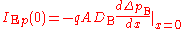
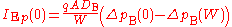
The DC emitter and collector currents in active mode are well modeled by an approximation to the Ebers–Moll model: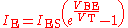


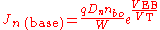
The base internal current is mainly by diffusion (see Fick's law) and
where
-
 is the thermal voltage
  (approximately 26 mV at 300 K ≈ room temperature).
 -
 is the emitter current
 -
 is the collector current
 -
 is the common base forward short circuit current gain (0.98 to 0.998)
 -
 is the reverse saturation current of the base–emitter diode (on the order of 10−15 to 10−12 amperes)
 -
 is the base–emitter voltage
 -
 is the diffusion constant for electrons in the p-type base
 - W is the base width
The
 and forward
  parameters are as described previously. A reverse
  is sometimes included in the model.
The unapproximated Ebers–Moll equations used to describe the three currents in any operating region are given below. These equations are based on the transport model for a bipolar junction transistor.
where
-
 is the collector current
 -
 is the base current
 -
 is the emitter current
 -
 is the forward common emitter current gain (20 to 500)
 -
 is the reverse common emitter current gain (0 to 20)
 -
 is the reverse saturation current (on the order of 10−15 to 10−12 amperes)
 -
 is the thermal voltage (approximately 26 mV at 300 K ≈ room temperature).
 -
 is the base–emitter voltage
 -
 is the base–collector voltage
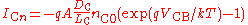
Base-width modulation
As the applied collector–base voltage (
 ) varies, the collector–base depletion region varies in size. An increase in the collector–base voltage, for example, causes a greater reverse bias across the collector–base junction, increasing the collector–base depletion region width, and decreasing the width of the base. This variation in base width often is called the "Early effect
Early Effect
The Early effect is the variation in the width of the base in a bipolar junction transistor due to a variation in the applied base-to-collector voltage, named after its discoverer James M. Early...
" after its discoverer James M. Early
James M. Early
James M. Early was an American engineer, best known for his work on transistors and charge-coupled device imagers. He is also known as Jim Early....
.
Narrowing of the base width has two consequences:
- There is a lesser chance for recombination within the "smaller" base region.
- The charge gradient is increased across the base, and consequently, the current of minority carriers injected across the emitter junction increases.
Both factors increase the collector or "output" current of the transistor in response to an increase in the collector–base voltage.
In the forward-active region, the Early effect modifies the collector current (
 ) and the forward common emitter current gain (
 ) as given by:
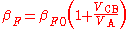

where:
-
 is the collector–emitter voltage
 -
 is the Early voltage (15 V to 150 V)
 -
 is forward common-emitter current gain when
  = 0 V
= 0 V -
 is the output impedance
 -
 is the collector current
Current–voltage characteristics
The following assumptions are involved when deriving ideal current-voltage characteristics of the BJT
- Low level injection
- Uniform doping in each region with abrupt junctions
- One-dimensional current
- Negligible recombination-generation in space charge regions
- Negligible electric fields outside of space charge regions.
It is important to characterize the minority diffusion currents induced by injection of carriers.
With regard to pn-junction diode, a key relation is the diffusion equation.
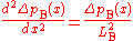
A solution of this equation is below, and two boundary conditions are used to solve and find
 and
and  .
.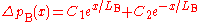
The following equations apply to the emitter and collector region, respectively, and the origins
 ,
,  , and
, and  apply to the base, collector, and emitter.

A boundary condition of the emitter is below:

The values of the constants
 and
and  are zero due to the following conditions of the emitter and collector regions as
  and
and  .
.

Because
 , the values of
  and
and  are
are  and
and  , respectively.

Expressions of
 and
and  can be evaluated.
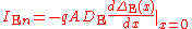
Because insignificant recombination occurs, the second derivative of
 is zero. There is therefore a linear relationship between excess hole density and
  .
.
The following are boundary conditions of
 .
.

Substitute into the above linear relation.
 .
.With this result, derive value of
 .
.
Use the expressions of
 ,
,  ,
,  , and
, and  to develop an expression of the emitter current.


Similarly, an expression of the collector current is derived.


An expression of the base current is found with the previous results.


Punchthrough
When the base–collector voltage reaches a certain (device specific) value, the base–collector depletion region boundary meets the base–emitter depletion region boundary. When in this state the transistor effectively has no base. The device thus loses all gain when in this state.
Gummel–Poon charge-control model
The Gummel–Poon modelGummel–Poon model
The Gummel–Poon model is a model of the bipolar junction transistor. It was first described in a paper published by Hermann Gummel and H. C. Poon at Bell Labs in 1970....
is a detailed charge-controlled model of BJT dynamics, which has been adopted and elaborated by others to explain transistor dynamics in greater detail than the terminal-based models typically do http://ece-www.colorado.edu/~bart/book/book/chapter5/ch5_6.htm#5_6_2. This model also includes the dependence of transistor
 -values upon the direct current levels in the transistor, which are assumed current-independent in the Ebers–Moll model.
h-parameter model
Another model commonly used to analyze BJT circuits is the "h-parameter" model, closely related to the hybrid-pi modelHybrid-pi model
The hybrid-pi model is a popular circuit model used for analyzing the small signal behavior of bipolar junction and field effect transistors. The model can be quite accurate for low-frequency circuits and can easily be adapted for higher frequency circuits with the addition of appropriate...
and the y-parameter
Admittance parameters
Admittance parameters or Y-parameters are properties used in electrical engineering, electronic engineering, and communication systems engineering describe the electrical behavior of linear electrical networks. They are also used to describe the small-signal response of non-linear networks...
two-port, but using input current and output voltage as independent variables, rather than input and output voltages. This two-port network is particularly suited to BJTs as it lends itself easily to the analysis of circuit behaviour, and may be used to develop further accurate models. As shown, the term "x" in the model represents a different BJT lead depending on the topology used. For common-emitter mode the various symbols take on the specific values as:
- x = 'e' because it is a common-emitter topology
- Terminal 1 = Base
- Terminal 2 = Collector
- Terminal 3 = Emitter
- ii = Base current (ib)
- io = Collector current (ic)
- Vin = Base-to-emitter voltage (VBE)
- Vo = Collector-to-emitter voltage (VCE)
and the h-parameters are given by:
- hix = hie – The input impedance of the transistor (corresponding to the base resistance rpi).
- hrx = hre – Represents the dependence of the transistor's IB–VBE curve on the value of VCE. It is usually very small and is often neglected (assumed to be zero).
- hfx = hfe – The current-gain of the transistor. This parameter is often specified as hFE or the DC current-gain (βDC) in datasheets.
- hox = 1/hoe – The output impedance of transistor. The parameter hoe usually corresponds to the output admittance of the bipolar transistor and has to be inverted to convert it to an impedance.
As shown, the h-parameters have lower-case subscripts and hence signify AC conditions or analyses. For DC conditions they are specified in upper-case. For the CE topology, an approximate h-parameter model is commonly used which further simplifies the circuit analysis. For this the hoe and hre parameters are neglected (that is, they are set to infinity and zero, respectively). It should also be noted that the h-parameter model as shown is suited to low-frequency, small-signal analysis. For high-frequency analyses the inter-electrode capacitances that are important at high frequencies must be added.
Etymology of hFE
The 'h' refers to its being an h-parameter, a set of parameters named for their origin in a hybrid equivalent circuit model. 'F' is from forward current amplification also called the current gain. 'E' refers to the transistor operating in a common emitter (CE) configuration. Capital letters used in the subscript indicate that hFE refers to a direct current circuit.
Applications
The BJT remains a device that excels in some applications, such as discrete circuit design, due to the very wide selection of BJT types available, and because of its high transconductanceTransconductance
Transconductance, also known as mutual conductance, is a property of certain electronic components. Conductance is the reciprocal of resistance; transconductance, meanwhile, is the ratio of the current change at the output port to the voltage change at the input port. It is written as gm...
and output resistance compared to MOSFET
MOSFET
The metal–oxide–semiconductor field-effect transistor is a transistor used for amplifying or switching electronic signals. The basic principle of this kind of transistor was first patented by Julius Edgar Lilienfeld in 1925...
s. The BJT is also the choice for demanding analog circuits, especially for very-high-frequency applications, such as radio-frequency circuits for wireless systems. Bipolar transistors can be combined with MOSFETs in an integrated circuit by using a BiCMOS
BiCMOS
BiCMOS is an evolved semiconductor technology that integrates two formerly separate semiconductor technologies - those of the analog bipolar junction transistor and the digital CMOS transistor - in a single integrated circuit device....
process of wafer fabrication to create circuits that take advantage of the application strengths of both types of transistor.
Temperature sensors
Because of the known temperature and current dependence of the forward-biased base–emitter junction voltage, the BJT can be used to measure temperature by subtracting two voltages at two different bias currents in a known ratio http://www.maxim-ic.com/appnotes.cfm/appnote_number/689.Logarithmic converters
Because base–emitter voltage varies as the log of the base–emitter and collector–emitter currents, a BJT can also be used to compute logarithmLogarithm
The logarithm of a number is the exponent by which another fixed value, the base, has to be raised to produce that number. For example, the logarithm of 1000 to base 10 is 3, because 1000 is 10 to the power 3: More generally, if x = by, then y is the logarithm of x to base b, and is written...
s and anti-logarithms. A diode can also perform these nonlinear functions, but the transistor provides more circuit flexibility.
Vulnerabilities
Exposure of the transistor to ionizing radiationIonizing radiation
Ionizing radiation is radiation composed of particles that individually have sufficient energy to remove an electron from an atom or molecule. This ionization produces free radicals, which are atoms or molecules containing unpaired electrons...
causes radiation damage
Radiation hardening
Radiation hardening is a method of designing and testing electronic components and systems to make them resistant to damage or malfunctions caused by ionizing radiation , such as would be encountered in outer space, high-altitude flight, around nuclear reactors, particle accelerators, or during...
. Radiation causes a buildup of 'defects' in the base region that act as recombination centers
Carrier generation and recombination
In the solid state physics of semiconductors, carrier generation and recombination are processes by which mobile charge carriers are created and eliminated. Carrier generation and recombination processes are fundamental to the operation of many optoelectronic semiconductor devices, such as...
. The resulting reduction in minority carrier lifetime causes gradual loss of gain of the transistor.
Power BJTs are subject to a failure mode called secondary breakdown, in which excessive current and normal imperfections in the silicon die cause portions of the silicon inside the device to become disproportionately hotter than the others. The doped silicon has a negative temperature coefficient
Temperature coefficient
The temperature coefficient is the relative change of a physical property when the temperature is changed by 1 K.In the following formula, let R be the physical property to be measured and T be the temperature at which the property is measured. T0 is the reference temperature, and ΔT is the...
, meaning that it conducts more current at higher temperatures. Thus, the hottest part of the die conducts the most current, causing its conductivity to increase, which then causes it to become progressively hotter again, until the device fails internally. The thermal runaway process associated with secondary breakdown, once triggered, occurs almost instantly and may catastrophically damage the transistor package.
If the emitter-base junction is reverse biased into avalanche
Avalanche breakdown
Avalanche breakdown is a phenomenon that can occur in both insulating and semiconducting materials. It is a form of electric current multiplication that can allow very large currents within materials which are otherwise good insulators. It is a type of electron avalanche...
or Zener mode and current flows for a short period of time, the current gain of the BJT will be permanently degraded.
See also
- Bipolar transistor biasingBipolar transistor biasingBipolar transistor amplifiers must be properly biased to operate correctly. In circuits made with individual devices , biasing networks consisting of resistors are commonly employed...
- Hybrid-pi modelHybrid-pi modelThe hybrid-pi model is a popular circuit model used for analyzing the small signal behavior of bipolar junction and field effect transistors. The model can be quite accurate for low-frequency circuits and can easily be adapted for higher frequency circuits with the addition of appropriate...
- TransistorTransistorA transistor is a semiconductor device used to amplify and switch electronic signals and power. It is composed of a semiconductor material with at least three terminals for connection to an external circuit. A voltage or current applied to one pair of the transistor's terminals changes the current...
- Transistor modelsTransistor modelsTransistors are simple devices with complicated behavior. In order to ensure the reliable operation of circuits employing transistors, it is necessary to scientifically model the physical phenomena observed in their operation using transistor models. There exists a variety of different models that...
- Technology CADTechnology CADTechnology CAD is a branch of electronic design automation that models semiconductor fabrication and semiconductor device operation. The modeling of the fabrication is termed Process TCAD, while the modeling of the device operation is termed Device TCAD...
(TCAD)
External links
- Simulation of a BJT in the Common Emitter Circuit
- Bipolar Transistors - The Transistor as a Switch
- Lessons In Electric Circuits – Bipolar Junction Transistors (Note: this site shows current as a flow of electrons, rather than the convention of showing it as a flow of holes, so the arrows may appear the other way around)
- EncycloBEAMia – Bipolar Junction Transistor
- Characteristic curves
- The transistor at play-hookey.com
- How Do Transistors Work? by William Beaty
- ENGI 242/ELEC 222: BJT Small Signal Models
- TRANSISTOR MUSEUM Historic Transistor Timeline
- ECE 327: Transistor Basics – Summarizes simple Ebers–Moll model of a bipolar transistor and gives several common BJT circuits.
- ECE 327: Procedures for Output Filtering Lab – Section 4 ("Power Amplifier") discusses design of a BJT-Sziklai-pair-based class-AB current driver in detail.
- BJT Operation description for undergraduate and first year graduate students to describe the basic principles of operation of Bipolar Junction Transistor.