

Polycrystalline silicon
Encyclopedia
Polycrystalline silicon, also called polysilicon, is a material consisting of small silicon
crystal
s. It differs from single-crystal silicon, used for electronics and solar cell
s, and from amorphous silicon
, used for thin film devices and solar cells.
 In single crystal silicon, the crystalline framework is homogenous, which can be recognized by an even external colouring. In single crystal silicon, also called monocrystal, the crystal lattice of the entire sample is continuous and unbroken with no grain boundaries. Large single crystals are exceedingly rare in nature and can also be difficult to produce in the laboratory (see also recrystallisation
). In contrast, in an amorphous structure the order in atomic positions is limited to short range.
Polycrystalline
and paracrystalline
phases (see Polycrystal) are composed of a number of smaller crystals or crystallite
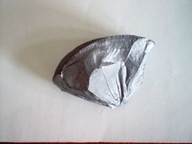
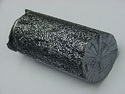
s. Polycrystalline silicon (or semicrystalline silicon, polysilicon, poly-Si, or simply "poly") is a material consisting of multiple small silicon
crystal
s. Polycrystalline cells can be recognized by a visible grain, a “metal flake effect”. Semiconductor grade (also solar grade) polycrystalline silicon is converted to "single crystal" silicon – meaning that the randomly associated crystallites of silicon in "polycrystalline silicon" are converted to a large "single" crystal. Single crystal silicon is used to manufacture most Si-based microelectronic devices. Polycrystalline silicon can be as much as 99.9999% pure. Ultra-pure poly is used in the semiconductor
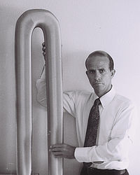
industry, starting from poly rods that are five to eight feet in length. In microelectronic industry (semiconductor industry), poly is used both at the macro-scale and micro-scale (component) level. Single crystal
s are grown using the Czochralski process
, float-zone
and Bridgman techniques.
 Polysilicon is a key component for integrated circuit
and central processing unit
manufacturers such as AMD and Intel.
At the component level, polysilicon has long been used as the conducting gate material in MOSFET
and CMOS
processing technologies. For these technologies it is deposited using low-pressure chemical-vapour deposition (LPCVD
) reactors at high temperatures and is usually heavily doped n-type
or p-type
.
More recently, intrinsic and doped polysilicon is being used in large-area electronics as the active and/or doped layers in thin-film transistor
s. Although it can be deposited by LPCVD
, plasma-enhanced chemical vapour deposition (PECVD
), or solid-phase crystallization (SPC) of amorphous silicon
in certain processing regimes, these processes still require relatively high temperatures of at least 300 °C. These temperatures make deposition of polysilicon possible for glass
substrates but not for plastic
substrates. The deposition of polycrystalline silicon on plastic substrates is motivated by the desire to be able to manufacture digital displays on flexible screens. Therefore, a relatively new technique called laser crystallization has been devised to crystallize a precursor amorphous silicon
(a-Si) material on a plastic substrate without melting or damaging the plastic. Short, high-intensity ultraviolet
laser
pulses are used to heat the deposited a-Si material to above the melting point of silicon, without melting the entire substrate. The molten silicon will then crystallize as it cools. By precisely controlling the temperature gradients, researchers have been able to grow very large grains, of up to hundreds of micrometers in size in the extreme case, although grain sizes of 10 nanometers to 1 micrometer
are also common. In order to create devices on polysilicon over large-areas however, a crystal grain size smaller than the device feature size is needed for homogeneity of the devices. Another method to produce poly-Si at low temperatures is metal-induced crystallization
where an amorphous-Si thin film can be crystallized at temperatures as low as 150C if annealed while in contact of another metal film such as aluminium
, gold
, or silver
.
 Polysilicon has many applications in VLSI manufacturing. One of its primary uses is as gate electrode material for MOS devices. A polysilicon gate's electrical conductivity may be increased by depositing a metal (such as tungsten) or a metal silicide (such as tungsten silicide) over the gate. Polysilicon may also be employed as a resistor, a conductor, or as an ohmic contact for shallow junctions, with the desired electrical conductivity attained by doping the polysilicon material.
One major difference between polysilicon and a-Si is that the mobility of the charge carrier
s of the polysilicon can be orders of magnitude larger and the material also shows greater stability under electric field
and light-induced stress. This allows more complex, high-speed circuity to be created on the glass substrate along with the a-Si devices, which are still needed for their low-leakage
characteristics. When polysilicon and a-Si devices are used in the same process this is called hybrid processing. A complete polysilicon active layer process is also used in some cases where a small pixel size is required, such as in projection displays
.
construction. Growth of the photovoltaic solar industry was limited by the supply of the polysilicon material. For the first time, in 2006, over half of the world's supply of polysilicon was being used for production of renewable electricity solar power
panels. Only twelve factories were known to produce solar-grade polysilicon in 2008. Monocrystalline silicon was higher priced and more efficient than multicrystalline. This however changed and, in 2011, there was a large excess of production capacity of polysilicon.
(SiH4) at 580 to 650 °C. This pyrolysis process releases hydrogen.
Polysilicon layers can be deposited using 100% silane at a pressure of 25–130 Pa (0.2 to 1.0 Torr) or with 20–30% silane (diluted in nitrogen) at the same total pressure. Both of these processes can deposit polysilicon on 10–200 wafers per run, at a rate of 10–20 nm/min and with thickness uniformities of ±5%. Critical process variables for polysilicon deposition include temperature, pressure, silane concentration, and dopant concentration. Wafer spacing and load size have been shown to have only minor effects on the deposition process. The rate of polysilicon deposition increases rapidly with temperature, since it follows Arrhenius
behavior, that is deposition rate = A·exp(–qEa/kT) where q is electron charge and k is the Boltzmann constant. The activation energy (Ea) for polysilicon deposition is about 1.7 eV. Based on this equation, the rate of polysilicon deposition increases as the deposition temperature increases. There will be a minimum temperature, however, wherein the rate of deposition becomes faster than the rate at which unreacted silane arrives at the surface. Beyond this temperature, the deposition rate can no longer increase with temperature, since it is now being hampered by lack of silane from which the polysilicon will be generated. Such a reaction is then said to be 'mass-transport-limited.' When a polysilicon deposition process becomes mass-transport-limited, the reaction rate becomes dependent primarily on reactant concentration, reactor geometry, and gas flow.
When the rate at which polysilicon deposition occurs is slower than the rate at which unreacted silane arrives, then it is said to be surface-reaction-limited. A deposition process that is surface-reaction-limited is primarily dependent on reactant concentration and reaction temperature. Deposition processes must be surface-reaction-limited because they result in excellent thickness uniformity and step coverage. A plot of the logarithm of the deposition rate against the reciprocal of the absolute temperature in the surface-reaction-limited region results in a straight line whose slope is equal to –qEa/k.
At reduced pressure levels for VLSI manufacturing, polysilicon deposition rate below 575 °C is too slow to be practical. Above 650 °C, poor deposition uniformity and excessive roughness will be encountered due to unwanted gas-phase reactions and silane depletion. Pressure can be varied inside a low-pressure reactor either by changing the pumping speed or changing the inlet gas flow into the reactor. If the inlet gas is composed of both silane and nitrogen, the inlet gas flow, and hence the reactor pressure, may be varied either by changing the nitrogen flow at constant silane flow, or changing both the nitrogen and silane flow to change the total gas flow while keeping the gas ratio constant.
Polysilicon doping, if needed, is also done during the deposition process, usually by adding phosphine, arsine, or diborane. Adding phosphine or arsine results in slower deposition, while adding diborane increases the deposition rate. The deposition thickness uniformity usually degrades when dopants are added during deposition.
is being produced as a low cost alternative to polysilicon created by the Siemens process. UMG greatly reduces impurities in a variety of ways that require less equipment and energy than the Siemens process. UMG is about 99% pure which is three or more orders of magnitude less pure and about 10 times less expensive than polysilicon ($1.70 to $3.20 per kg from 2005 to 2008 compared to $40 to $400 per kg for polysilicon). It has the potential to provide nearly-as-good solar cell efficiency at 1/5 the capital expenditure, half the energy requirements, and less than $15/kg.
In 2008 several companies were touting the potential of UMG in 2010, but the credit crisis greatly lowered the cost of polysilicon and several UMG producers put plans on hold. The Siemens process will remain the dominant form of production for years to come due to more efficiently implementing the Siemens process. GT Solar claims a new Siemens process can produce at $27/kg and may reach $20/kg in 5 years. GCL-Poly expects production costs to be $20/kg by end of 2011. Elkem Solar estimates their UMG costs to be $25/kg, with a capacity of 6,000 tonnes by the end of 2010. Calisolar expects UMG technology to produce at $12/kg in 5 years with boron at 0.3 ppm and phosphorus at 0.6 ppm. At $50/kg and 7.5 g/W, module manufacturers spend $0.37/W for the polysilicon. For comparison, if a CdTe manufacturer pays spot price for tellurium ($420/kg in April 2010) and has a 3 micron thickness, their cost would be 10 times less, $0.037/Watt. At 0.1 g/W and $31/ozt for silver, polysilicon solar producers spend $0.10/W on silver.
Q-Cells, Canadian Solar, and Calisolar have used Timminco UMG. Timminco is able to produce UMG-Si with 0.5 ppm boron for $21/kg but were sued by shareholders because they had expected $10/kg. RSI and Dow Corning have also been in litigation over UMG-Si technology.
in July 2011, the total polysilicon production in 2010 was 209,000 tons and first-tier suppliers account for 64% of the market while China-based polysilicon firms have 30% of market share. The total production is likely to increase 37.4% to 281,000 tons by end of 2011. With high spot price
s in 2008/2009 and lack of available material, many companies announced additional capacities for the coming years. Established producers (mentioned below) expand their capacities, additionally newcomers – especially from Asia – are moving into this market. Even long-time players in the field had difficulties recently to ramp-up new plants. It is yet unclear which companies will be able to produce at costs low enough to be profitable after the steep drop in spot-prices of the last months.
Leading producer capacities:
Silicon
Silicon is a chemical element with the symbol Si and atomic number 14. A tetravalent metalloid, it is less reactive than its chemical analog carbon, the nonmetal directly above it in the periodic table, but more reactive than germanium, the metalloid directly below it in the table...
crystal
Crystal
A crystal or crystalline solid is a solid material whose constituent atoms, molecules, or ions are arranged in an orderly repeating pattern extending in all three spatial dimensions. The scientific study of crystals and crystal formation is known as crystallography...
s. It differs from single-crystal silicon, used for electronics and solar cell
Solar cell
A solar cell is a solid state electrical device that converts the energy of light directly into electricity by the photovoltaic effect....
s, and from amorphous silicon
Amorphous silicon
Amorphous silicon is the non-crystalline allotropic form of silicon. It can be deposited in thin films at low temperatures onto a variety of substrates, offering some unique capabilities for a variety of electronics.-Description:...
, used for thin film devices and solar cells.
Single crystalline vs polycrystalline silicon
Recrystallization (chemistry)
-Chemistry:In chemistry, recrystallization is a procedure for purifying compounds. The most typical situation is that a desired "compound A" is contaminated by a small amount of "impurity B". There are various methods of purification that may be attempted , which includes recrystallization...
). In contrast, in an amorphous structure the order in atomic positions is limited to short range.
Polycrystalline
Polycrystalline
Polycrystalline materials are solids that are composed of many crystallites of varying size and orientation. The variation in direction can be random or directed, possibly due to growth and processing conditions. Fiber texture is an example of the latter.Almost all common metals, and many ceramics...
and paracrystalline
Paracrystalline
Paracrystalline materials are defined as having short and medium range ordering in their lattice but lacking long-range ordering at least in one direction....
phases (see Polycrystal) are composed of a number of smaller crystals or crystallite
Crystallite
Crystallites are small, often microscopic crystals that, held together through highly defective boundaries, constitute a polycrystalline solid. Metallurgists often refer to crystallites as grains.- Details :...
s. Polycrystalline silicon (or semicrystalline silicon, polysilicon, poly-Si, or simply "poly") is a material consisting of multiple small silicon
Silicon
Silicon is a chemical element with the symbol Si and atomic number 14. A tetravalent metalloid, it is less reactive than its chemical analog carbon, the nonmetal directly above it in the periodic table, but more reactive than germanium, the metalloid directly below it in the table...
crystal
Crystal
A crystal or crystalline solid is a solid material whose constituent atoms, molecules, or ions are arranged in an orderly repeating pattern extending in all three spatial dimensions. The scientific study of crystals and crystal formation is known as crystallography...
s. Polycrystalline cells can be recognized by a visible grain, a “metal flake effect”. Semiconductor grade (also solar grade) polycrystalline silicon is converted to "single crystal" silicon – meaning that the randomly associated crystallites of silicon in "polycrystalline silicon" are converted to a large "single" crystal. Single crystal silicon is used to manufacture most Si-based microelectronic devices. Polycrystalline silicon can be as much as 99.9999% pure. Ultra-pure poly is used in the semiconductor
Semiconductor
A semiconductor is a material with electrical conductivity due to electron flow intermediate in magnitude between that of a conductor and an insulator. This means a conductivity roughly in the range of 103 to 10−8 siemens per centimeter...
industry, starting from poly rods that are five to eight feet in length. In microelectronic industry (semiconductor industry), poly is used both at the macro-scale and micro-scale (component) level. Single crystal
Single crystal
A single crystal or monocrystalline solid is a material in which the crystal lattice of the entire sample is continuous and unbroken to the edges of the sample, with no grain boundaries...
s are grown using the Czochralski process
Czochralski process
The Czochralski process is a method of crystal growth used to obtain single crystals of semiconductors , metals , salts, and synthetic gemstones...
, float-zone
Float-zone silicon
Float-zone silicon is very pure silicon obtained by vertical zone melting. The process was developed at Bell Labs by Henry Theuerer in 1955 as a modification of a method developed by William Gardner Pfann for germanium. In the vertical configuration molten silicon has sufficient surface tension to...
and Bridgman techniques.
Polycrystalline silicon components
Integrated circuit
An integrated circuit or monolithic integrated circuit is an electronic circuit manufactured by the patterned diffusion of trace elements into the surface of a thin substrate of semiconductor material...
and central processing unit
Central processing unit
The central processing unit is the portion of a computer system that carries out the instructions of a computer program, to perform the basic arithmetical, logical, and input/output operations of the system. The CPU plays a role somewhat analogous to the brain in the computer. The term has been in...
manufacturers such as AMD and Intel.
At the component level, polysilicon has long been used as the conducting gate material in MOSFET
MOSFET
The metal–oxide–semiconductor field-effect transistor is a transistor used for amplifying or switching electronic signals. The basic principle of this kind of transistor was first patented by Julius Edgar Lilienfeld in 1925...
and CMOS
CMOS
Complementary metal–oxide–semiconductor is a technology for constructing integrated circuits. CMOS technology is used in microprocessors, microcontrollers, static RAM, and other digital logic circuits...
processing technologies. For these technologies it is deposited using low-pressure chemical-vapour deposition (LPCVD
Chemical vapor deposition
Chemical vapor deposition is a chemical process used to produce high-purity, high-performance solid materials. The process is often used in the semiconductor industry to produce thin films. In a typical CVD process, the wafer is exposed to one or more volatile precursors, which react and/or...
) reactors at high temperatures and is usually heavily doped n-type
N-type semiconductor
N-type semiconductors are a type of extrinsic semiconductor where the dopant atoms are capable of providing extra conduction electrons to the host material . This creates an excess of negative electron charge carriers....
or p-type
P-type semiconductor
A P-type semiconductor is obtained by carrying out a process of doping: that is, adding a certain type of atoms to the semiconductor in order to increase the number of free charge carriers ....
.
More recently, intrinsic and doped polysilicon is being used in large-area electronics as the active and/or doped layers in thin-film transistor
Thin-film transistor
A thin-film transistor is a special kind of field-effect transistor made by depositing thin films of a semiconductor active layer as well as the dielectric layer and metallic contacts over a supporting substrate. A common substrate is glass, since the primary application of TFTs is in liquid...
s. Although it can be deposited by LPCVD
Chemical vapor deposition
Chemical vapor deposition is a chemical process used to produce high-purity, high-performance solid materials. The process is often used in the semiconductor industry to produce thin films. In a typical CVD process, the wafer is exposed to one or more volatile precursors, which react and/or...
, plasma-enhanced chemical vapour deposition (PECVD
Chemical vapor deposition
Chemical vapor deposition is a chemical process used to produce high-purity, high-performance solid materials. The process is often used in the semiconductor industry to produce thin films. In a typical CVD process, the wafer is exposed to one or more volatile precursors, which react and/or...
), or solid-phase crystallization (SPC) of amorphous silicon
Amorphous silicon
Amorphous silicon is the non-crystalline allotropic form of silicon. It can be deposited in thin films at low temperatures onto a variety of substrates, offering some unique capabilities for a variety of electronics.-Description:...
in certain processing regimes, these processes still require relatively high temperatures of at least 300 °C. These temperatures make deposition of polysilicon possible for glass
Glass
Glass is an amorphous solid material. Glasses are typically brittle and optically transparent.The most familiar type of glass, used for centuries in windows and drinking vessels, is soda-lime glass, composed of about 75% silica plus Na2O, CaO, and several minor additives...
substrates but not for plastic
Plastic
A plastic material is any of a wide range of synthetic or semi-synthetic organic solids used in the manufacture of industrial products. Plastics are typically polymers of high molecular mass, and may contain other substances to improve performance and/or reduce production costs...
substrates. The deposition of polycrystalline silicon on plastic substrates is motivated by the desire to be able to manufacture digital displays on flexible screens. Therefore, a relatively new technique called laser crystallization has been devised to crystallize a precursor amorphous silicon
Amorphous silicon
Amorphous silicon is the non-crystalline allotropic form of silicon. It can be deposited in thin films at low temperatures onto a variety of substrates, offering some unique capabilities for a variety of electronics.-Description:...
(a-Si) material on a plastic substrate without melting or damaging the plastic. Short, high-intensity ultraviolet
Ultraviolet
Ultraviolet light is electromagnetic radiation with a wavelength shorter than that of visible light, but longer than X-rays, in the range 10 nm to 400 nm, and energies from 3 eV to 124 eV...
laser
Laser
A laser is a device that emits light through a process of optical amplification based on the stimulated emission of photons. The term "laser" originated as an acronym for Light Amplification by Stimulated Emission of Radiation...
pulses are used to heat the deposited a-Si material to above the melting point of silicon, without melting the entire substrate. The molten silicon will then crystallize as it cools. By precisely controlling the temperature gradients, researchers have been able to grow very large grains, of up to hundreds of micrometers in size in the extreme case, although grain sizes of 10 nanometers to 1 micrometer
Micrometer
A micrometer , sometimes known as a micrometer screw gauge, is a device incorporating a calibrated screw used widely for precise measurement of small distances in mechanical engineering and machining as well as most mechanical trades, along with other metrological instruments such as dial, vernier,...
are also common. In order to create devices on polysilicon over large-areas however, a crystal grain size smaller than the device feature size is needed for homogeneity of the devices. Another method to produce poly-Si at low temperatures is metal-induced crystallization
Metal-induced crystallization
Metal-induced crystallization is a method by which amorphous silicon, or a-Si, can be turned into polycrystalline silicon at relatively low temperatures. In MIC an amorphous Si film is deposited onto a substrate, usually glass or Si, and then capped with a metal, such as aluminium...
where an amorphous-Si thin film can be crystallized at temperatures as low as 150C if annealed while in contact of another metal film such as aluminium
Aluminium
Aluminium or aluminum is a silvery white member of the boron group of chemical elements. It has the symbol Al, and its atomic number is 13. It is not soluble in water under normal circumstances....
, gold
Gold
Gold is a chemical element with the symbol Au and an atomic number of 79. Gold is a dense, soft, shiny, malleable and ductile metal. Pure gold has a bright yellow color and luster traditionally considered attractive, which it maintains without oxidizing in air or water. Chemically, gold is a...
, or silver
Silver
Silver is a metallic chemical element with the chemical symbol Ag and atomic number 47. A soft, white, lustrous transition metal, it has the highest electrical conductivity of any element and the highest thermal conductivity of any metal...
.
One major difference between polysilicon and a-Si is that the mobility of the charge carrier
Charge carrier
In physics, a charge carrier is a free particle carrying an electric charge, especially the particles that carry electric currents in electrical conductors. Examples are electrons and ions...
s of the polysilicon can be orders of magnitude larger and the material also shows greater stability under electric field
Electric field
In physics, an electric field surrounds electrically charged particles and time-varying magnetic fields. The electric field depicts the force exerted on other electrically charged objects by the electrically charged particle the field is surrounding...
and light-induced stress. This allows more complex, high-speed circuity to be created on the glass substrate along with the a-Si devices, which are still needed for their low-leakage
Leakage
Leakage may refer to:*Leakage *Memory leak, in computer science*Leakage *Leakage *Leakage *Leakage...
characteristics. When polysilicon and a-Si devices are used in the same process this is called hybrid processing. A complete polysilicon active layer process is also used in some cases where a small pixel size is required, such as in projection displays
Liquid crystal on silicon
Liquid crystal on silicon is a "micro-projection" or "micro-display" technology typically applied in projection televisions. It is a reflective technology similar to DLP projectors; however, it uses liquid crystals instead of individual mirrors. By way of comparison, LCD projectors use...
.
Solar panel and applications
Polycrystalline silicon is also a key component of solar panelPhotovoltaic module
A solar panel is a packaged, connected assembly of solar cells, also known as photovoltaic cells...
construction. Growth of the photovoltaic solar industry was limited by the supply of the polysilicon material. For the first time, in 2006, over half of the world's supply of polysilicon was being used for production of renewable electricity solar power
Solar power
Solar energy, radiant light and heat from the sun, has been harnessed by humans since ancient times using a range of ever-evolving technologies. Solar radiation, along with secondary solar-powered resources such as wind and wave power, hydroelectricity and biomass, account for most of the available...
panels. Only twelve factories were known to produce solar-grade polysilicon in 2008. Monocrystalline silicon was higher priced and more efficient than multicrystalline. This however changed and, in 2011, there was a large excess of production capacity of polysilicon.
Deposition methods
Polysilicon deposition, or the process of depositing a layer of polycrystalline silicon on a semiconductor wafer, is achieved by pyrolyzing silaneSilane
Silane is a toxic, extremely flammable chemical compound with chemical formula SiH4. In 1857, the German chemists and Friedrich Woehler discovered silane among the products formed by the action of hydrochloric acid on aluminum silicide, which they had previously prepared...
(SiH4) at 580 to 650 °C. This pyrolysis process releases hydrogen.
Polysilicon layers can be deposited using 100% silane at a pressure of 25–130 Pa (0.2 to 1.0 Torr) or with 20–30% silane (diluted in nitrogen) at the same total pressure. Both of these processes can deposit polysilicon on 10–200 wafers per run, at a rate of 10–20 nm/min and with thickness uniformities of ±5%. Critical process variables for polysilicon deposition include temperature, pressure, silane concentration, and dopant concentration. Wafer spacing and load size have been shown to have only minor effects on the deposition process. The rate of polysilicon deposition increases rapidly with temperature, since it follows Arrhenius
Arrhenius equation
The Arrhenius equation is a simple, but remarkably accurate, formula for the temperature dependence of the reaction rate constant, and therefore, rate of a chemical reaction. The equation was first proposed by the Dutch chemist J. H. van 't Hoff in 1884; five years later in 1889, the Swedish...
behavior, that is deposition rate = A·exp(–qEa/kT) where q is electron charge and k is the Boltzmann constant. The activation energy (Ea) for polysilicon deposition is about 1.7 eV. Based on this equation, the rate of polysilicon deposition increases as the deposition temperature increases. There will be a minimum temperature, however, wherein the rate of deposition becomes faster than the rate at which unreacted silane arrives at the surface. Beyond this temperature, the deposition rate can no longer increase with temperature, since it is now being hampered by lack of silane from which the polysilicon will be generated. Such a reaction is then said to be 'mass-transport-limited.' When a polysilicon deposition process becomes mass-transport-limited, the reaction rate becomes dependent primarily on reactant concentration, reactor geometry, and gas flow.
When the rate at which polysilicon deposition occurs is slower than the rate at which unreacted silane arrives, then it is said to be surface-reaction-limited. A deposition process that is surface-reaction-limited is primarily dependent on reactant concentration and reaction temperature. Deposition processes must be surface-reaction-limited because they result in excellent thickness uniformity and step coverage. A plot of the logarithm of the deposition rate against the reciprocal of the absolute temperature in the surface-reaction-limited region results in a straight line whose slope is equal to –qEa/k.
At reduced pressure levels for VLSI manufacturing, polysilicon deposition rate below 575 °C is too slow to be practical. Above 650 °C, poor deposition uniformity and excessive roughness will be encountered due to unwanted gas-phase reactions and silane depletion. Pressure can be varied inside a low-pressure reactor either by changing the pumping speed or changing the inlet gas flow into the reactor. If the inlet gas is composed of both silane and nitrogen, the inlet gas flow, and hence the reactor pressure, may be varied either by changing the nitrogen flow at constant silane flow, or changing both the nitrogen and silane flow to change the total gas flow while keeping the gas ratio constant.
Polysilicon doping, if needed, is also done during the deposition process, usually by adding phosphine, arsine, or diborane. Adding phosphine or arsine results in slower deposition, while adding diborane increases the deposition rate. The deposition thickness uniformity usually degrades when dopants are added during deposition.
Upgraded metallurgical-grade silicon
Upgraded metallurgical-grade (UMG) silicon (also known as UMG-Si) solar cellSolar cell
A solar cell is a solid state electrical device that converts the energy of light directly into electricity by the photovoltaic effect....
is being produced as a low cost alternative to polysilicon created by the Siemens process. UMG greatly reduces impurities in a variety of ways that require less equipment and energy than the Siemens process. UMG is about 99% pure which is three or more orders of magnitude less pure and about 10 times less expensive than polysilicon ($1.70 to $3.20 per kg from 2005 to 2008 compared to $40 to $400 per kg for polysilicon). It has the potential to provide nearly-as-good solar cell efficiency at 1/5 the capital expenditure, half the energy requirements, and less than $15/kg.
In 2008 several companies were touting the potential of UMG in 2010, but the credit crisis greatly lowered the cost of polysilicon and several UMG producers put plans on hold. The Siemens process will remain the dominant form of production for years to come due to more efficiently implementing the Siemens process. GT Solar claims a new Siemens process can produce at $27/kg and may reach $20/kg in 5 years. GCL-Poly expects production costs to be $20/kg by end of 2011. Elkem Solar estimates their UMG costs to be $25/kg, with a capacity of 6,000 tonnes by the end of 2010. Calisolar expects UMG technology to produce at $12/kg in 5 years with boron at 0.3 ppm and phosphorus at 0.6 ppm. At $50/kg and 7.5 g/W, module manufacturers spend $0.37/W for the polysilicon. For comparison, if a CdTe manufacturer pays spot price for tellurium ($420/kg in April 2010) and has a 3 micron thickness, their cost would be 10 times less, $0.037/Watt. At 0.1 g/W and $31/ozt for silver, polysilicon solar producers spend $0.10/W on silver.
Q-Cells, Canadian Solar, and Calisolar have used Timminco UMG. Timminco is able to produce UMG-Si with 0.5 ppm boron for $21/kg but were sued by shareholders because they had expected $10/kg. RSI and Dow Corning have also been in litigation over UMG-Si technology.
Manufacturers
Capacity
Polysilicon manufacturing market is in a very fast growth mode. According to DigitimesDigiTimes
DigiTimes is a daily newspaper for semiconductor, electronics, computer and communications industries in Taiwan and the Greater China region. It was established in 1998...
in July 2011, the total polysilicon production in 2010 was 209,000 tons and first-tier suppliers account for 64% of the market while China-based polysilicon firms have 30% of market share. The total production is likely to increase 37.4% to 281,000 tons by end of 2011. With high spot price
Spot price
The spot price or spot rate of a commodity, a security or a currency is the price that is quoted for immediate settlement . Spot settlement is normally one or two business days from trade date...
s in 2008/2009 and lack of available material, many companies announced additional capacities for the coming years. Established producers (mentioned below) expand their capacities, additionally newcomers – especially from Asia – are moving into this market. Even long-time players in the field had difficulties recently to ramp-up new plants. It is yet unclear which companies will be able to produce at costs low enough to be profitable after the steep drop in spot-prices of the last months.
Leading producer capacities:
- Hemlock SemiconductorHemlock Semiconductor CorporationHemlock Semiconductor Corporation, named after Hemlock, Michigan, is the largest producer of polysilicon in the United States. It is a subsidiary of Dow Corning and was founded in 1961....
(2010: 36 kt) USA. $3 billion expansion mulled in addition to $1.2 billion expansion due in 2012. - Wacker Chemie (2011: 32 kt, Jan 2012: 42kt, Jan 2014: 67 kt) GermanyGermanyGermany , officially the Federal Republic of Germany , is a federal parliamentary republic in Europe. The country consists of 16 states while the capital and largest city is Berlin. Germany covers an area of 357,021 km2 and has a largely temperate seasonal climate...
. - GCL-PolyGCL-Poly Energy Holdings LimitedGCL-Poly is one of the leading green energy suppliers in China, providing power and heat via cogeneration, incineration and wind. GCL-Poly is also one of the leading polysilicon and wafer suppliers in the world, delivering silicon products to the solar industry.In November 2009, China Investment...
(2010: 21 kt, Jan 2012: 46 kt ) Hong KongHong KongHong Kong is one of two Special Administrative Regions of the People's Republic of China , the other being Macau. A city-state situated on China's south coast and enclosed by the Pearl River Delta and South China Sea, it is renowned for its expansive skyline and deep natural harbour...
. - OCIOCI (company)OCI or OCI Company Ltd is a Korean conglomerate based in Seoul. It was founded in 1959 as "Oriental Chemical Industries". It manufactures inorganic chemicals, coal, petrochemicals, and fine chemicals. Its inorganic chemicals products consist of hydrogen peroxide, soda ash, sodium carbonate,...
(June 2010: 17 kt, Dec 2010: 27 kt, Jan 2012: 42 kt, Oct 2012: 62 kt) South KoreaSouth KoreaThe Republic of Korea , , is a sovereign state in East Asia, located on the southern portion of the Korean Peninsula. It is neighbored by the People's Republic of China to the west, Japan to the east, North Korea to the north, and the East China Sea and Republic of China to the south...
. - Renewable Energy CorporationRenewable Energy CorporationThe Renewable Energy Corporation is a solar power company with headquarters in Norway. REC produces silicon materials for photovoltaics applications and multicrystalline wafers, as well as solar cells and modules...
ASA (REC) (2010: 17kt) NorwayNorwayNorway , officially the Kingdom of Norway, is a Nordic unitary constitutional monarchy whose territory comprises the western portion of the Scandinavian Peninsula, Jan Mayen, and the Arctic archipelago of Svalbard and Bouvet Island. Norway has a total area of and a population of about 4.9 million...
. - LDK Solar (2010: 15kt) China.
- Tokuyama (2009: 8 kt, Jan 2013: 11 kt, 2015: 31kt) JapanJapanJapan is an island nation in East Asia. Located in the Pacific Ocean, it lies to the east of the Sea of Japan, China, North Korea, South Korea and Russia, stretching from the Sea of Okhotsk in the north to the East China Sea and Taiwan in the south...
. - MEMC Electronic MaterialsMEMC Electronic MaterialsMEMC Electronic Materials is a United States manufacturer of silicon wafers for the semiconductor industry. The company's stock is part of the S&P 500 stock index. Originally established in 1959 as the Monsanto Electronic Materials Company, a business unit of Monsanto Company, the company is...
(2010: 8 kt, Jan 2013: 18 kt) USA. - Hankook Silicon (2011: 3.2 kt, 2013: 14.5 kt)
- Nitol SolarNitol SolarNitol Solar is an international, vertically integrated company originating from Russia whose main business activities are scientific development and manufacture of products used to generate solar energy.They were valued at $1bn in Jan 2008...
, (2011: 5 kt, Jan 2011), Russia - Mitsubishi Polysilicon (2008: 4.3 kt)
- Sumitomo Titanium (now Osaka Titanium) (2008: 4.2 kt)
- Daqo, (2011: 4.3kt, under construction 3kt), China
- Beijing Lier High-temperature Materials Co, (2012: 5kt)
- Qatar Solar Technologies, at Ras Laffan, announced an 8,000 mt facility for start in 2013.
Price
Prices of polysilicon are often divided into two categories, contract and spot prices. While in booming installation times, price rally occurs in polysilicon. Not only spot prices surpass contract prices in the market; but it is also hard to acquire enough polysilicon. Buyers will accept down payment and long term agreements to acquire a large enough volume of polysilicon. On the contrary, spot prices will be below contract prices once the solar PV installation is in a down trend. In late 2010, booming installation brought up the spot prices of polysilicon. In the first half of 2011, prices of polysilicon kept strong owing to the FIT policies of Italy. The solar PV price survey and market research firm, PVinsights, reported that the prices of polysilicon might be dragged down by lack of installation in the second half of 2011.See also
- Bulk
- Cadmium tellurideCadmium tellurideCadmium telluride is a crystalline compound formed from cadmium and tellurium. It is used as an infrared optical window and a solar cell material. It is usually sandwiched with cadmium sulfide to form a p-n junction photovoltaic solar cell...
- Low-cost solar cell
- Metallurgical grade silicon
- Nanocrystalline siliconNanocrystalline siliconNanocrystalline silicon , sometimes also known as microcrystalline silicon , is a form of porous silicon. It is an allotropic form of silicon with paracrystalline structure—is similar to amorphous silicon , in that it has an amorphous phase...
- Polycrystal
- Photovoltaic cells
- Photovoltaic modulePhotovoltaic moduleA solar panel is a packaged, connected assembly of solar cells, also known as photovoltaic cells...
- Wafer (electronics)Wafer (electronics)A wafer is a thin slice of semiconductor material, such as a silicon crystal, used in the fabrication of integrated circuits and other microdevices...