
CMOS
Encyclopedia
Integrated circuit
An integrated circuit or monolithic integrated circuit is an electronic circuit manufactured by the patterned diffusion of trace elements into the surface of a thin substrate of semiconductor material...
s. CMOS technology is used in microprocessor
Microprocessor
A microprocessor incorporates the functions of a computer's central processing unit on a single integrated circuit, or at most a few integrated circuits. It is a multipurpose, programmable device that accepts digital data as input, processes it according to instructions stored in its memory, and...
s, microcontroller
Microcontroller
A microcontroller is a small computer on a single integrated circuit containing a processor core, memory, and programmable input/output peripherals. Program memory in the form of NOR flash or OTP ROM is also often included on chip, as well as a typically small amount of RAM...
s, static RAM
Static random access memory
Static random-access memory is a type of semiconductor memory where the word static indicates that, unlike dynamic RAM , it does not need to be periodically refreshed, as SRAM uses bistable latching circuitry to store each bit...
, and other digital logic circuits. CMOS technology is also used for several analog circuits such as image sensor
Image sensor
An image sensor is a device that converts an optical image into an electronic signal. It is used mostly in digital cameras and other imaging devices...
s (CMOS sensor), data converters
Data conversion
Data conversion is the conversion of computer data from one format to another. Throughout a computer environment, data is encoded in a variety of ways. For example, computer hardware is built on the basis of certain standards, which requires that data contains, for example, parity bit checks....
, and highly integrated transceiver
Transceiver
A transceiver is a device comprising both a transmitter and a receiver which are combined and share common circuitry or a single housing. When no circuitry is common between transmit and receive functions, the device is a transmitter-receiver. The term originated in the early 1920s...
s for many types of communication. Frank Wanlass
Frank Wanlass
Frank Marion Wanlass was an electrical engineer. He obtained his PhD from the University of Utah. He invented CMOS logic circuits in 1963 while working at Fairchild Semiconductor. He was given U.S. patent #3,356,858 for "Low Stand-By Power Complementary Field Effect Circuitry" in 1967...
patented CMOS in 1967 (US patent 3,356,858).
CMOS is also sometimes referred to as complementary-symmetry metal–oxide–semiconductor (or COS-MOS).
The words "complementary-symmetry" refer to the fact that the typical digital design style with CMOS uses complementary and symmetrical pairs of p-type
P-type semiconductor
A P-type semiconductor is obtained by carrying out a process of doping: that is, adding a certain type of atoms to the semiconductor in order to increase the number of free charge carriers ....
and n-type
N-type semiconductor
N-type semiconductors are a type of extrinsic semiconductor where the dopant atoms are capable of providing extra conduction electrons to the host material . This creates an excess of negative electron charge carriers....
metal oxide semiconductor field effect transistors (MOSFETs) for logic functions.
Two important characteristics of CMOS devices are high noise immunity
Electronic noise
Electronic noise is a random fluctuation in an electrical signal, a characteristic of all electronic circuits. Noise generated by electronic devices varies greatly, as it can be produced by several different effects...
and low static power consumption. Significant power is only drawn when the transistor
Transistor
A transistor is a semiconductor device used to amplify and switch electronic signals and power. It is composed of a semiconductor material with at least three terminals for connection to an external circuit. A voltage or current applied to one pair of the transistor's terminals changes the current...
s in the CMOS device are switching between on and off states. Consequently, CMOS devices do not produce as much waste heat
Waste heat
Waste heat sometimes called Secondary heat or Low-grade heat refers to heat produced by machines, electrical equipment and industrial processes for which no useful application is found. Energy is often produced by a heat engine, running on a source of high-temperature heat...
as other forms of logic, for example transistor-transistor logic
Transistor-transistor logic
Transistor–transistor logic is a class of digital circuits built from bipolar junction transistors and resistors. It is called transistor–transistor logic because both the logic gating function and the amplifying function are performed by transistors .TTL is notable for being a widespread...
(TTL) or NMOS logic
NMOS logic
N-type metal-oxide-semiconductor logic uses n-type metal-oxide-semiconductor field effect transistors to implement logic gates and other digital circuits...
. CMOS also allows a high density of logic functions on a chip. It was primarily for this reason that CMOS became the most used technology to be implemented in VLSI chips.
The phrase "metal–oxide–semiconductor" is a reference to the physical structure of certain field-effect transistor
Field-effect transistor
The field-effect transistor is a transistor that relies on an electric field to control the shape and hence the conductivity of a channel of one type of charge carrier in a semiconductor material. FETs are sometimes called unipolar transistors to contrast their single-carrier-type operation with...
s, having a metal gate electrode placed on top of an oxide insulator, which in turn is on top of a semiconductor material
Semiconductor
A semiconductor is a material with electrical conductivity due to electron flow intermediate in magnitude between that of a conductor and an insulator. This means a conductivity roughly in the range of 103 to 10−8 siemens per centimeter...
. Aluminum was once used but now the material is polysilicon. Other metal gate
Metal gate
A metal gate, in the context of a lateral Metal-Oxide-Semiconductor MOS stack, is just that—the gate material is made from a metal.For decades, the industry had moved away from metal as the gate material in the MOS stack due to fabrication complications...
s have made a comeback with the advent of high-k dielectric materials in the CMOS process, as announced by IBM and Intel for the 45 nanometer
45 nanometer
Per the International Technology Roadmap for Semiconductors, the 45 nm technology node should refer to the average half-pitch of a memory cell manufactured at around the 2007–2008 time frame....
node and beyond.
Technical details
"CMOS" refers to both a particular style of digital circuitry design, and the family of processes used to implement that circuitry on integrated circuits (chips). CMOS circuitry dissipates less powerLow-power electronics
Low-power electronics means that the consumption of electric power is deliberately low, e.g. notebook processors.- Computing elements :The density and speed of integrated-circuit computing elements have increased exponentially for several decades, following a trend described by Moore's Law...
than logic families with resistive loads. Since this advantage has increased and grown more important, CMOS processes and variants have come to dominate, thus the vast majority of modern integrated circuit manufacturing is on CMOS processes.
As of 2010, CPUs with the best performance per watt
Performance per watt
In computing, performance per watt is a measure of the energy efficiency of a particular computer architecture or computer hardware. Literally, it measures the rate of computation that can be delivered by a computer for every watt of power consumed....
each year have been CMOS static logic since 1976.
CMOS circuits use a combination of p-type and n-type metal–oxide–semiconductor field-effect transistor
MOSFET
The metal–oxide–semiconductor field-effect transistor is a transistor used for amplifying or switching electronic signals. The basic principle of this kind of transistor was first patented by Julius Edgar Lilienfeld in 1925...
s (MOSFETs) to implement logic gate
Logic gate
A logic gate is an idealized or physical device implementing a Boolean function, that is, it performs a logical operation on one or more logic inputs and produces a single logic output. Depending on the context, the term may refer to an ideal logic gate, one that has for instance zero rise time and...
s and other digital circuit
Digital circuit
Digital electronics represent signals by discrete bands of analog levels, rather than by a continuous range. All levels within a band represent the same signal state...
s found in computer
Computer
A computer is a programmable machine designed to sequentially and automatically carry out a sequence of arithmetic or logical operations. The particular sequence of operations can be changed readily, allowing the computer to solve more than one kind of problem...
s, telecommunication
Telecommunication
Telecommunication is the transmission of information over significant distances to communicate. In earlier times, telecommunications involved the use of visual signals, such as beacons, smoke signals, semaphore telegraphs, signal flags, and optical heliographs, or audio messages via coded...
s equipment, and signal processing
Signal processing
Signal processing is an area of systems engineering, electrical engineering and applied mathematics that deals with operations on or analysis of signals, in either discrete or continuous time...
equipment. Although CMOS logic can be implemented with discrete devices (e.g., for instructional purposes in an introductory circuits class), typical commercial CMOS products are integrated circuits composed of millions of transistors of both types on a rectangular piece of silicon of between 10 and 400mm2. These devices are commonly called "chip
Integrated circuit
An integrated circuit or monolithic integrated circuit is an electronic circuit manufactured by the patterned diffusion of trace elements into the surface of a thin substrate of semiconductor material...
s", although within the industry they are also referred to as a "die
Die (integrated circuit)
A die in the context of integrated circuits is a small block of semiconducting material, on which a given functional circuit is fabricated.Typically, integrated circuits are produced in large batches on a single wafer of electronic-grade silicon or other semiconductor through processes such as...
" (singular) or "dice", or "dies" (plural).
Composition
The main principle behind CMOS circuits that allows them to implement logic gateLogic gate
A logic gate is an idealized or physical device implementing a Boolean function, that is, it performs a logical operation on one or more logic inputs and produces a single logic output. Depending on the context, the term may refer to an ideal logic gate, one that has for instance zero rise time and...
s is the use of p-type and n-type metal–oxide–semiconductor field-effect transistor
MOSFET
The metal–oxide–semiconductor field-effect transistor is a transistor used for amplifying or switching electronic signals. The basic principle of this kind of transistor was first patented by Julius Edgar Lilienfeld in 1925...
s to create paths to the output from either the voltage source or ground. When a path to output is created from the voltage source, the circuit is said to be pulled up. The other circuit state occurs when a path to output is created from ground and the output pulled down to the ground potential.
Inversion
Electrical resistance
The electrical resistance of an electrical element is the opposition to the passage of an electric current through that element; the inverse quantity is electrical conductance, the ease at which an electric current passes. Electrical resistance shares some conceptual parallels with the mechanical...
between its source and drain contacts when a low gate
Gate
A gate is a point of entry to a space enclosed by walls, or a moderately sized opening in a fence. Gates may prevent or control entry or exit, or they may be merely decorative. Other terms for gate include yett and port...
voltage
Voltage
Voltage, otherwise known as electrical potential difference or electric tension is the difference in electric potential between two points — or the difference in electric potential energy per unit charge between two points...
is applied and high resistance when a high gate voltage is applied. On the other hand, the composition of an NMOS transistor creates high resistance between source and drain when a low gate voltage is applied and low resistance when a high gate voltage is applied. CMOS accomplishes current reduction by complementing every nMOSFET with a pMOSFET and connecting both gates and both drains together. A high voltage on the gates will cause the nMOSFET to conduct and the pMOSFET not to conduct while a low voltage on the gates causes the reverse. This arrangement greatly reduces power consumption and heat generation. However, during the switching time both MOSFETs conduct briefly as the voltage goes from one state to another. This induces a brief spike in power consumption and becomes a serious issue at high frequencies.
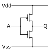
The image on the right shows what happens when an input is connected to both a PMOS transistor (top of diagram) and an NMOS transistor (bottom of diagram). When the voltage of input A is low, the NMOS transistor's channel is in a high resistance state. This limits the current that can flow from Q to ground. The PMOS transistor's channel is in a low resistance state and much more current can flow from the supply to the output. Because the resistance between the supply voltage and Q is low, the voltage drop between the supply voltage and Q due to a current drawn from Q is small. The output therefore registers a high voltage.
On the other hand, when the voltage of input A is high, the PMOS transistor is in an OFF (high resistance) state so it would limit the current flowing from the positive supply to the output, while the NMOS transistor is in an ON (low resistance) state, allowing the output to drain to ground. Because the resistance between Q and ground is low, the voltage drop due to a current drawn into Q placing Q above ground is small. This low drop results in the output registering a low voltage.
In short, the outputs of the PMOS and NMOS transistors are complementary such that when the input is low, the output is high, and when the input is high, the output is low. Because of this behavior of input and output, the CMOS circuits' output is the inversion of the input.
A note on nomenclature: The power supplies for CMOS are called VDD and VSS, or VCC and Ground(GND) depending on the manufacturer. VDD and VSS are carryovers from conventional MOS circuits and stand for the drain and source supplies. These do not apply directly to CMOS since both supplies are really source supplies. VCC and Ground are carryovers from TTL logic and that nomenclature has been retained with the introduction of the 54C/74C line of CMOS.
Duality
An important characteristic of a CMOS circuit is the duality that exists between its PMOS transistors and NMOS transistors. A CMOS circuit is created to allow a path always to exist from the output to either the power source or ground. To accomplish this, the set of all paths to the voltage source must be the complement of the set of all paths to ground. This can be easily accomplished by defining one in terms of the NOT of the other. Due to the De Morgan's laws based logic, the PMOS transistors in parallel have corresponding NMOS transistors in series while the PMOS transistors in series have corresponding NMOS transistors in parallel.Logic
Logical disjunction
In logic and mathematics, a two-place logical connective or, is a logical disjunction, also known as inclusive disjunction or alternation, that results in true whenever one or more of its operands are true. E.g. in this context, "A or B" is true if A is true, or if B is true, or if both A and B are...
gates require manipulating the paths between gates to represent the logic. When a path consists of two transistors in series, both transistors must have low resistance to the corresponding supply voltage, modeling an AND. When a path consists of two transistors in parallel, either one or both of the transistors must have low resistance to connect the supply voltage to the output, modeling an OR.
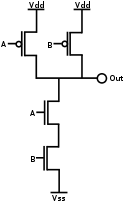
Shown on the right is a circuit diagram
Circuit diagram
A circuit diagram is a simplified conventional graphical representation of an electrical circuit...
of a NAND gate
NAND gate
The Negated AND, NO AND or NAND gate is the opposite of the digital AND gate, and behaves in a manner that corresponds to the opposite of AND gate, as shown in the truth table on the right. A LOW output results only if both the inputs to the gate are HIGH...
in CMOS logic. If both of the A and B inputs are high, then both the NMOS transistors (bottom half of the diagram) will conduct, neither of the PMOS transistors (top half) will conduct, and a conductive path will be established between the output and Vss (ground), bringing the output low. If either of the A or B inputs is low, one of the NMOS transistors will not conduct, one of the PMOS transistors will, and a conductive path will be established between the output and Vdd (voltage source), bringing the output high.
An advantage of CMOS over NMOS is that both low-to-high and high-to-low output transitions are fast since the pull-up transistors have low resistance when switched on, unlike the load resistors in NMOS logic. In addition, the output signal swings the full voltage
Voltage
Voltage, otherwise known as electrical potential difference or electric tension is the difference in electric potential between two points — or the difference in electric potential energy per unit charge between two points...
between the low and high rails. This strong, more nearly symmetric response also makes CMOS more resistant to noise.
See Logical effort
Logical effort
The method of logical effort, a term coined by Ivan Sutherland and Bob Sproull in 1991, is a straightforward technique used to estimate delay in a CMOS circuit...
for a method of calculating delay in a CMOS circuit.
Example: NAND gate in physical layout
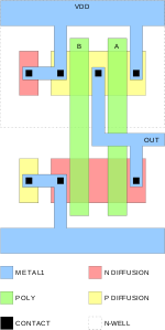
The inputs to the NAND
NAND gate
The Negated AND, NO AND or NAND gate is the opposite of the digital AND gate, and behaves in a manner that corresponds to the opposite of AND gate, as shown in the truth table on the right. A LOW output results only if both the inputs to the gate are HIGH...
(illustrated in green color) are in polysilicon. The CMOS transistors (devices) are formed by the intersection of the polysilicon and diffusion; N diffusion for the N device & P diffusion for the P device (illustrated in salmon and yellow coloring respectively). The output ("out") is connected together in metal (illustrated in cyan coloring). Connections between metal and polysilicon or diffusion are made through contacts (illustrated as black squares). The physical layout example matches the NAND logic circuit given in the previous example.
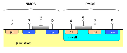
The N device is manufactured on a P-type substrate while the P device is manufactured in an N-type well (n-well). A P-type substrate "tap" is connected to VSS and an N-type n-well tap is connected to VDD to prevent latchup
Latchup
Latchup is a term used in the realm of integrated circuits to describe a particular type of short circuit which can occur in an improperly designed circuit...
.
Power: switching and leakage
CMOS logic dissipates less power than NMOS logic circuits because CMOS dissipates power only when switching ("dynamic power"). On a typical ASICApplication-specific integrated circuit
An application-specific integrated circuit is an integrated circuit customized for a particular use, rather than intended for general-purpose use. For example, a chip designed solely to run a cell phone is an ASIC...
in a modern 90 nanometer
90 nanometer
The 90 nm process refers to the level of CMOS process technology that was reached in the 2002–2003 timeframe, by most leading semiconductor companies, like Intel, AMD, Infineon, Texas Instruments, IBM, and TSMC....
process, switching the output might take 120 picoseconds, and happen once every ten nanoseconds. NMOS logic dissipates power whenever the transistor is on, because there is a current path from Vdd to Vss through the load resistor and the n-type network.
Static CMOS gates are very power efficient because they dissipate nearly zero power when idle. Earlier, the power consumption of CMOS devices was not the major concern while designing chips. Factors like speed and area dominated the design parameters. As the CMOS technology moved below sub-micron levels the power consumption per unit area of the chip has risen tremendously.
Broadly classifying, power dissipation in CMOS circuits occurs because of two components:
- Static dissipation
- Sub threshold condition when the transistors are off.
Both NMOS and PMOS transistors have a gate–source threshold voltageThreshold voltageThe threshold voltage of a MOSFET is usually defined as the gate voltage where an inversion layer forms at the interface between the insulating layer and the substrate of the transistor. The purpose of the inversion layer's forming is to allow the flow of electrons through the gate-source junction...
, below which the current (called sub threshold current) through the device drops exponentially. Historically, CMOS designs operated at supply voltages much larger than their threshold voltages (Vdd might have been 5 V, and Vth for both NMOS and PMOS might have been 700 mV). A special type of the CMOS transistor with near zero threshold voltageThreshold voltageThe threshold voltage of a MOSFET is usually defined as the gate voltage where an inversion layer forms at the interface between the insulating layer and the substrate of the transistor. The purpose of the inversion layer's forming is to allow the flow of electrons through the gate-source junction...
is the native transistorNative transistorIn electronics, a native transistor is a variety of the MOS field-effect transistor that is intermediate between enhancement and depletion modes...
.
- Tunnelling current through gate oxide.
SiO2 is a very good insulator, but at very small thickness levels electrons can tunnel across the very thin insulation; the probability drops off exponentially with oxide thickness. Tunnelling current becomes very important for transistors below 130 nm technology with gate oxides of 20 Å or thinner.
- Leakage current through reverse biased diodes.
Small reverse leakage currents are formed due to formation of reverse bias between diffusion regions and wells (for e.g., p-type diffusion vs. n-well), wells and substrate (for e.g., n-well vs. p-substrate). In modern process diode leakage is very small compared to sub threshold and tunnelling currents, so these may be neglected during power calculations.
- Contention current in ratioed circuit
- Dynamic Dissipation
- Charging and discharging of load capacitances.
CMOS circuits dissipate power by charging the various load capacitances (mostly gate and wire capacitance, but also drain and some source capacitances) whenever they are switched. In one complete cycle of CMOS logic, current flows from VDD to the load capacitance to charge it and then flows from the charged load capacitance to ground during discharge. Therefore in one complete charge/discharge cycle, a total of Q=CLVDD is thus transferred from VDD to ground. Multiply by the switching frequency on the load capacitances to get the current used, and multiply by voltage again to get the characteristic switching power dissipated by a CMOS device: .
.
Since most gates do not operate/switch at every clock cycle, they are often accompanied by a factor , called the activity factor. Now, the dynamic power dissipation may be re-written as
  .
.
A clock in a system has an activity factor α=1, since it rises and falls every cycle. Most data has an activity factor of 0.5. If correct load capacitance is estimated on a node together with its activity factor, the dynamic power dissipation at that node can be calculated effectively.
- Short circuit power dissipation
Since there is a finite rise/fall time for both pMOS and nMOS, during transition, for example, from off to on, both the transistors will be on for a small period of time in which current will find a path directly from VDD to ground, hence creating a short circuit current. Short circuit power dissipation increases with rise and fall time of the transistors.
An additional form of power consumption became significant in the 1990s as wires on chip became narrower and the long wires became more resistive. CMOS gates at the end of those resistive wires see slow input transitions. During the middle of these transitions, both the NMOS and PMOS logic networks are partially conductive, and current flows directly from Vdd to VSS. The power thus used is called crowbar power. Careful design which avoids weakly driven long skinny wires has ameliorated this effect, and crowbar power is nearly always substantially smaller than switching power.
To speed up designs, manufacturers have switched to constructions that have lower voltage thresholds but because of this a modern NMOS transistor with a Vth of 200 mV has a significant subthreshold leakage
Subthreshold leakage
The Subthreshold conduction or the subthreshold leakage or the subthreshold drain current is the current that flows between the source and drain of a MOSFET when the transistor is in subthreshold region, or weak-inversion region, that is, for gate-to-source voltages below the threshold voltage. The...
current. Designs (e.g. desktop processors) which include vast numbers of circuits which are not actively switching still consume power because of this leakage current. Leakage power is a significant portion of the total power consumed by such designs. Further technology advances that use even thinner gate dielectrics have an additional leakage component because of current tunnelling through the extremely thin gate dielectric. Using high-k dielectric
High-k Dielectric
The term high-κ dielectric refers to a material with a high dielectric constant κ used in semiconductor manufacturing processes which replaces the silicon dioxide gate dielectric...
s instead of silicon dioxide
Silicon dioxide
The chemical compound silicon dioxide, also known as silica , is an oxide of silicon with the chemical formula '. It has been known for its hardness since antiquity...
that is the conventional gate dielectric allows similar device performance, but with a thicker gate insulator, thus avoiding this current. Leakage power reduction using new material and system designs is critical to sustaining scaling of CMOS.
Analog CMOS
Besides digital applications, CMOS technology is also used in analogAnalogue electronics
Analogue electronics are electronic systems with a continuously variable signal, in contrast to digital electronics where signals usually take only two different levels. The term "analogue" describes the proportional relationship between a signal and a voltage or current that represents the signal...
applications. For example, there are CMOS operational amplifier
Operational amplifier
An operational amplifier is a DC-coupled high-gain electronic voltage amplifier with a differential input and, usually, a single-ended output...
ICs available in the market. Transmission gates may be used instead of signal relay
Relay
A relay is an electrically operated switch. Many relays use an electromagnet to operate a switching mechanism mechanically, but other operating principles are also used. Relays are used where it is necessary to control a circuit by a low-power signal , or where several circuits must be controlled...
s. CMOS technology is also widely used for RF
Radio frequency
Radio frequency is a rate of oscillation in the range of about 3 kHz to 300 GHz, which corresponds to the frequency of radio waves, and the alternating currents which carry radio signals...
circuits all the way to microwave frequencies, in mixed-signal
Mixed-signal integrated circuit
A mixed-signal integrated circuit is any integrated circuit that has both analog circuits and digital circuits on a single semiconductor die.- Examples :...
(analog+digital) applications.
Temperature range
Conventional CMOS devices work over a range of −55 °C to +125 °C. There were theoretical indications as early as August 2008 that silicon CMOS will work down to −233 °C (40 KKelvin
The kelvin is a unit of measurement for temperature. It is one of the seven base units in the International System of Units and is assigned the unit symbol K. The Kelvin scale is an absolute, thermodynamic temperature scale using as its null point absolute zero, the temperature at which all...
). Functioning temperatures near 40 K have since been achieved using overclocked AMD Phenom II
Phenom II
Phenom II is a family of AMD's multi-core 45 nm processors using the AMD K10 microarchitecture, succeeding the original Phenom. Advanced Micro Devices released the Socket AM2+ version of Phenom II in December 2008, while Socket AM3 versions with DDR3 support, along with an initial batch of...
processors with a combination of liquid nitrogen and liquid helium cooling.
See also
- FEOLFEOLFEOL denotes the first portion of IC fabrication where the individual devices are patterned in the semiconductor...
- PCMOSPCMOSPCMOS is a semiconductor manufacturing technology invented by Pr. Krishna Palem of Rice University and Director of NTU's Institute for Sustainable Nanoelectronics . The technology hopes to compete against current CMOS technology...
- MOSFETMOSFETThe metal–oxide–semiconductor field-effect transistor is a transistor used for amplifying or switching electronic signals. The basic principle of this kind of transistor was first patented by Julius Edgar Lilienfeld in 1925...
- HCMOSHCMOSHCMOS, high-speed CMOS, is the set of specifications for electrical ratings and characteristics, forming the 74HC00 family, a part of the 7400 series of integrated circuits....
- Active pixel sensorActive pixel sensorAn active-pixel sensor is an image sensor consisting of an integrated circuit containing an array of pixel sensors, each pixel containing a photodetector and an active amplifier. There are many types of active pixel sensors including the CMOS APS used most commonly in cell phone cameras, web...
- Gate equivalent (GE)Gate equivalentA gate equivalent stands for a unit of measure which allows to specify manufacturing-technology-independent complexity of digital electronic circuits....
- ElectricElectric (software)The Electric VLSI Design System is an EDA tool written by Steven M. Rubin.Electric is used to draw schematics and to do integrated circuit layout.It can also handle hardware description languages such as VHDL and Verilog....
and MagicMagic (software)Magic is a Very-large-scale integration layout tool originally written by John Ousterhout and his graduate students at UC Berkeley during the 1980s. Magic continues to be popular because it is free , easy to use, and easy to expand for specialized tasks...
are open-source software often used to lay out CMOS circuits.
External links
- CMOS gate description and interactive illustrations
- LASI is a "general purpose" IC layout CAD tool. It is a free download and can be used as a layout tool for CMOS circuits.