Feedback amplifier
Encyclopedia
A negative feedback amplifier (or more commonly simply a feedback amplifier) is an amplifier which combines a fraction of the output with the input so that a negative feedback
opposes the original signal. The applied negative feedback improves performance (gain stability, linearity, frequency response, step response
) and reduces sensitivity to parameter variations due to manufacturing or environment. Because of these advantages, negative feedback is used in this way in many amplifiers and control systems.
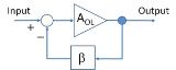
A negative feedback amplifier is a system of three elements (see Figure 1): an amplifier with gain AOL, an attenuating feedback network with a constant β < 1 and a summing circuit acting as a subtractor (the circle in the figure). The amplifier is the only obligatory; the other elements may be omitted in some cases. For example, in a voltage (emitter, source
, op-amp) follower the feedback network and the summing circuit are not necessary.
s, bipolar transistors, MOS transistors
) are nonlinear. Negative feedback allows gain
to be traded for higher linearity (reducing distortion
), amongst other things. If not designed correctly amplifiers with negative feedback can become unstable, resulting in unwanted behavior, such as oscillation
. The Nyquist stability criterion
developed by Harry Nyquist
of Bell Laboratories can be used to study the stability of feedback amplifiers.
Feedback amplifiers share these properties:
Pros:
Cons:
(US patent 2,102,671 (issued in 1937) ) while a passenger on the Lackawanna Ferry (from Hoboken Terminal to Manhattan) on his way to work at Bell Laboratories (historically located in Manhattan instead of New Jersey in 1927) on August 2, 1927. Black had been toiling at reducing distortion
in repeater
amplifiers used for telephone transmission. On a blank space in his copy of The New York Times, he recorded the diagram found in Figure 1, and the equations derived below.
Black submitted his invention to the U. S. Patent Office on August 8, 1928, and it took more than nine years for the patent to be issued. Black later wrote: "One reason for the delay was that the concept was so contrary to established beliefs that the Patent Office initially did not believe it would work."
two resistors forming a voltage divider may be used for the feedback network to set β between 0 and 1. This network may be modified using reactive elements like capacitor
s or inductor
s to (a) give frequency-dependent closed-loop gain as in equalization/tone-control circuits or (b) construct oscillators. The gain of the amplifier with feedback is derived below in the case of a voltage amplifier with voltage feedback.
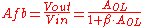
Without feedback, the input voltage V'in is applied directly to the amplifier input. The according output voltage is
Suppose now that an attenuating feedback loop applies a fraction β.Vout of the output to one of the subtractor inputs so that it subtracts from the circuit input voltage Vin applied to the other subtractor input. The result of subtraction applied to the amplifier input is

Substituting for V'in in the first expression,

Rearranging

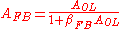
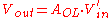
Then the gain of the amplifier with feedback, called the closed-loop gain, Afb is given by,
If AOL >> 1, then Afb ≈ 1 / β and the effective amplification (or closed-loop gain) Afb is set by the feedback constant β, and hence set by the feedback network, usually a simple reproducible network, thus making linearizing and stabilizing the amplification characteristics straightforward. Note also that if there are conditions where β AOL = −1, the amplifier has infinite amplification – it has become an oscillator, and the system is unstable. The stability characteristics of the gain feedback product β AOL are often displayed and investigated on a Nyquist plot
(a polar plot of the gain/phase shift as a parametric function of frequency). A simpler, but less general technique, uses Bode plots.
The combination L = β AOL appears commonly in feedback analysis and is called the loop gain. The combination ( 1 + β AOL ) also appears commonly and is variously named as the desensitivity factor or the improvement factor.
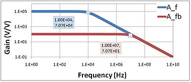 Feedback can be used to extend the bandwidth of an amplifier (speed it up) at the cost of lowering the amplifier gain. Figure 2 shows such a comparison. The figure is understood as follows. Without feedback the so-called open-loop gain in this example has a single time constant frequency response given by
where fC is the cutoff
or corner frequency of the amplifier: in this example fC = 104 Hz and the gain at zero frequency A0 = 105 V/V. The figure shows the gain is flat out to the corner frequency and then drops. When feedback is present the so-called closed-loop gain, as shown in the formula of the previous section, becomes,
Negative feedback
Negative feedback occurs when the output of a system acts to oppose changes to the input of the system, with the result that the changes are attenuated. If the overall feedback of the system is negative, then the system will tend to be stable.- Overview :...
opposes the original signal. The applied negative feedback improves performance (gain stability, linearity, frequency response, step response
Step response
The step response of a system in a given initial state consists of the time evolution of its outputs when its control inputs are Heaviside step functions. In electronic engineering and control theory, step response is the time behaviour of the outputs of a general system when its inputs change from...
) and reduces sensitivity to parameter variations due to manufacturing or environment. Because of these advantages, negative feedback is used in this way in many amplifiers and control systems.
A negative feedback amplifier is a system of three elements (see Figure 1): an amplifier with gain AOL, an attenuating feedback network with a constant β < 1 and a summing circuit acting as a subtractor (the circle in the figure). The amplifier is the only obligatory; the other elements may be omitted in some cases. For example, in a voltage (emitter, source
Common drain
In electronics, a common-drain amplifier, also known as a source follower, is one of three basic single-stage field effect transistor amplifier topologies, typically used as a voltage buffer. In this circuit the gate terminal of the transistor serves as the input, the source is the output, and the...
, op-amp) follower the feedback network and the summing circuit are not necessary.
Overview
Fundamentally, all electronic devices used to provide power gain (e.g. vacuum tubeVacuum tube
In electronics, a vacuum tube, electron tube , or thermionic valve , reduced to simply "tube" or "valve" in everyday parlance, is a device that relies on the flow of electric current through a vacuum...
s, bipolar transistors, MOS transistors
Fet
Fet is a municipality in Akershus county, Norway. It is part of the Romerike traditional region. The administrative centre of the municipality is the village of Fetsund.Fet was established as a municipality on 1 January 1838...
) are nonlinear. Negative feedback allows gain
Gain
In electronics, gain is a measure of the ability of a circuit to increase the power or amplitude of a signal from the input to the output. It is usually defined as the mean ratio of the signal output of a system to the signal input of the same system. It may also be defined on a logarithmic scale,...
to be traded for higher linearity (reducing distortion
Distortion
A distortion is the alteration of the original shape of an object, image, sound, waveform or other form of information or representation. Distortion is usually unwanted, and often many methods are employed to minimize it in practice...
), amongst other things. If not designed correctly amplifiers with negative feedback can become unstable, resulting in unwanted behavior, such as oscillation
Oscillation
Oscillation is the repetitive variation, typically in time, of some measure about a central value or between two or more different states. Familiar examples include a swinging pendulum and AC power. The term vibration is sometimes used more narrowly to mean a mechanical oscillation but sometimes...
. The Nyquist stability criterion
Nyquist stability criterion
When designing a feedback control system, it is generally necessary to determine whether the closed-loop system will be stable. An example of a destabilizing feedback control system would be a car steering system that overcompensates -- if the car drifts in one direction, the control system...
developed by Harry Nyquist
Harry Nyquist
Harry Nyquist was an important contributor to information theory.-Personal life:...
of Bell Laboratories can be used to study the stability of feedback amplifiers.
Feedback amplifiers share these properties:
Pros:
- Can increase or decrease input impedanceElectrical impedanceElectrical impedance, or simply impedance, is the measure of the opposition that an electrical circuit presents to the passage of a current when a voltage is applied. In quantitative terms, it is the complex ratio of the voltage to the current in an alternating current circuit...
(depending on type of feedback) - Can increase or decrease output impedance (depending on type of feedback)
- Reduces distortion (increases linearity)
- Increases the bandwidth
- Desensitizes gain to component variations
- Can control step responseStep responseThe step response of a system in a given initial state consists of the time evolution of its outputs when its control inputs are Heaviside step functions. In electronic engineering and control theory, step response is the time behaviour of the outputs of a general system when its inputs change from...
of amplifier
Cons:
- May lead to instability if not designed carefully
- The gain of the amplifier decreases
- The input and output impedances of the amplifier with feedback (the closed-loop amplifier) become sensitive to the gain of the amplifier without feedback (the open-loop amplifier); that exposes these impedances to variations in the open loop gain, for example, due to parameter variations or due to nonlinearity of the open-loop gain
History
The negative feedback amplifier was invented by Harold Stephen BlackHarold Stephen Black
Harold Stephen Black was an American electrical engineer, who revolutionized the field of applied electronics by inventing the negative feedback amplifier in 1927. To some, his invention is considered the most important breakthrough of the twentieth century in the field of electronics, since it...
(US patent 2,102,671 (issued in 1937) ) while a passenger on the Lackawanna Ferry (from Hoboken Terminal to Manhattan) on his way to work at Bell Laboratories (historically located in Manhattan instead of New Jersey in 1927) on August 2, 1927. Black had been toiling at reducing distortion
Distortion
A distortion is the alteration of the original shape of an object, image, sound, waveform or other form of information or representation. Distortion is usually unwanted, and often many methods are employed to minimize it in practice...
in repeater
Repeater
A repeater is an electronic device that receives asignal and retransmits it at a higher level and/or higher power, or onto the other side of an obstruction, so that the signal can cover longer distances.-Description:...
amplifiers used for telephone transmission. On a blank space in his copy of The New York Times, he recorded the diagram found in Figure 1, and the equations derived below.
Black submitted his invention to the U. S. Patent Office on August 8, 1928, and it took more than nine years for the patent to be issued. Black later wrote: "One reason for the delay was that the concept was so contrary to established beliefs that the Patent Office initially did not believe it would work."
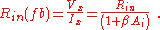
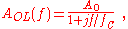
Gain reduction
Below, the voltage gain of the amplifier with feedback, the closed-loop gain Afb, is derived in terms of the gain of the amplifier without feedback, the open-loop gain AOL and the feedback factor β, which governs how much of the output signal is applied to the input. See Figure 1, top right. The open-loop gain AOL in general may be a function of both frequency and voltage; the feedback parameter β is determined by the feedback network that is connected around the amplifier. For an operational amplifierOperational amplifier
An operational amplifier is a DC-coupled high-gain electronic voltage amplifier with a differential input and, usually, a single-ended output...
two resistors forming a voltage divider may be used for the feedback network to set β between 0 and 1. This network may be modified using reactive elements like capacitor
Capacitor
A capacitor is a passive two-terminal electrical component used to store energy in an electric field. The forms of practical capacitors vary widely, but all contain at least two electrical conductors separated by a dielectric ; for example, one common construction consists of metal foils separated...
s or inductor
Inductor
An inductor is a passive two-terminal electrical component used to store energy in a magnetic field. An inductor's ability to store magnetic energy is measured by its inductance, in units of henries...
s to (a) give frequency-dependent closed-loop gain as in equalization/tone-control circuits or (b) construct oscillators. The gain of the amplifier with feedback is derived below in the case of a voltage amplifier with voltage feedback.
Without feedback, the input voltage V'in is applied directly to the amplifier input. The according output voltage is
Suppose now that an attenuating feedback loop applies a fraction β.Vout of the output to one of the subtractor inputs so that it subtracts from the circuit input voltage Vin applied to the other subtractor input. The result of subtraction applied to the amplifier input is
Substituting for V'in in the first expression,
Rearranging
Then the gain of the amplifier with feedback, called the closed-loop gain, Afb is given by,
If AOL >> 1, then Afb ≈ 1 / β and the effective amplification (or closed-loop gain) Afb is set by the feedback constant β, and hence set by the feedback network, usually a simple reproducible network, thus making linearizing and stabilizing the amplification characteristics straightforward. Note also that if there are conditions where β AOL = −1, the amplifier has infinite amplification – it has become an oscillator, and the system is unstable. The stability characteristics of the gain feedback product β AOL are often displayed and investigated on a Nyquist plot
Nyquist plot
A Nyquist plot is a parametric plot of a transfer function used in automatic control and signal processing. The most common use of Nyquist plots is for assessing the stability of a system with feedback. In Cartesian coordinates, the real part of the transfer function is plotted on the X axis. The...
(a polar plot of the gain/phase shift as a parametric function of frequency). A simpler, but less general technique, uses Bode plots.
The combination L = β AOL appears commonly in feedback analysis and is called the loop gain. The combination ( 1 + β AOL ) also appears commonly and is variously named as the desensitivity factor or the improvement factor.
Bandwidth extension
where fC is the cutoff
Cutoff frequency
In physics and electrical engineering, a cutoff frequency, corner frequency, or break frequency is a boundary in a system's frequency response at which energy flowing through the system begins to be reduced rather than passing through.Typically in electronic systems such as filters and...
or corner frequency of the amplifier: in this example fC = 104 Hz and the gain at zero frequency A0 = 105 V/V. The figure shows the gain is flat out to the corner frequency and then drops. When feedback is present the so-called closed-loop gain, as shown in the formula of the previous section, becomes,
-
-
-

The last expression shows the feedback amplifier still has a single time constant behavior, but the corner frequency is now increased by the improvement factor ( 1 + β A0 ), and the gain at zero frequency has dropped by exactly the same factor. This behavior is called the gain-bandwidth tradeoffGain-bandwidth productThe gain–bandwidth product for an amplifier is the product of the amplifier's bandwidth, and the gain at which the bandwidth is measured....
. In Figure 2, ( 1 + β A0 ) = 103, so Afb(0)= 105 / 103 = 100 V/V, and fC increases to 104 × 103 = 107 Hz.
Multiple poles
When the open-loop gain has several poles, rather than the single pole of the above example, feedback can result in complex poles (real and imaginary parts). In a two-pole case, the result is peaking in the frequency response of the feedback amplifier near its corner frequency, and ringingRinging artifactsIn signal processing, particularly digital image processing, ringing artifacts are artifacts that appear as spurious signals near sharp transitions in a signal. Visually, they appear as bands or "ghosts" near edges; audibly, they appear as "echos" near transients, particularly sounds from...
and overshootOvershoot (signal)In signal processing, control theory, electronics, and mathematics, overshoot is when a signal or function exceeds its target. It arises especially in the step response of bandlimited systems such as low-pass filters...
in its step responseStep responseThe step response of a system in a given initial state consists of the time evolution of its outputs when its control inputs are Heaviside step functions. In electronic engineering and control theory, step response is the time behaviour of the outputs of a general system when its inputs change from...
. In the case of more than two poles, the feedback amplifier can become unstable, and oscillate. See the discussion of gain margin and phase margin. For a complete discussion, see Sansen.
Asymptotic gain model
In the above analysis the feedback network is unilateral. However, real feedback networks often exhibit feed forward as well, that is, they feed a small portion of the input to the output, degrading performance of the feedback amplifier. A more general way to model negative feedback amplifiers including this effect is with the asymptotic gain model.
Feedback and amplifier type
Amplifiers use current or voltage as input and output, so four types of amplifier are possible. See classification of amplifiers. Any of these four choices may be the open-loop amplifier used to construct the feedback amplifier. The objective for the feedback amplifier also may be any one of the four types of amplifier, not necessarily the same type as the open-loop amplifier. For example, an op amp (voltage amplifier) can be arranged to make a current amplifier instead. The conversion from one type to another is implemented using different feedback connections, usually referred to as series or shunt (parallel) connections. See the table below.Feedback amplifier type Input connection Output connection Ideal feedback Two-port feedback Current Shunt Series CCCS g-parameter Transresistance Shunt Shunt CCVS y-parameter Transconductance Series Series VCCS z-parameter Voltage Series Shunt VCVS h-parameter
The feedback can be implemented using a two-port networkTwo-port networkA two-port network is an electrical circuit or device with two pairs of terminals connected together internally by an electrical network...
. There are four types of two-port network, and the selection depends upon the type of feedback. For example, for a current feedback amplifier, current at the output is sampled and combined with current at the input. Therefore, the feedback ideally is performed using an (output) current-controlled current source (CCCS), and its imperfect realization using a two-port network also must incorporate a CCCS, that is, the appropriate choice for feedback network is a g-parameter two-port.
Two-port analysis of feedback
One approach to feedback is the use of return ratioReturn ratioThe return ratio of a dependent source in a linear electrical circuit is the negative of the ratio of the current returned to the site of the dependent source to the current of a replacement independent source...
. Here an alternative method used in most textbooks is presented by means of an example treated in the article on asymptotic gain model.
Figure 3 shows a two-transistor amplifier with a feedback resistor Rf. The aim is to analyze this circuit to find three items: the gain, the output impedance looking into the amplifier from the load, and the input impedance looking into the amplifier from the source.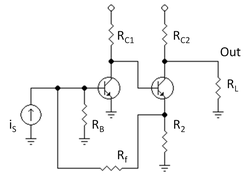
Replacement of the feedback network with a two-port
The first step is replacement of the feedback network by a two-portTwo-port networkA two-port network is an electrical circuit or device with two pairs of terminals connected together internally by an electrical network...
. Just what components go into the two-port?
On the input side of the two-port we have Rf. If the voltage at the right side of Rf changes, it changes the current in Rf that is subtracted from the current entering the base of the input transistor. That is, the input side of the two-port is a dependent current source controlled by the voltage at the top of resistor R2.
One might say the second stage of the amplifier is just a voltage follower, transmitting the voltage at the collector of the input transistor to the top of R2. That is, the monitored output signal is really the voltage at the collector of the input transistor. That view is legitimate, but then the voltage follower stage becomes part of the feedback network. That makes analysis of feedback more complicated.
An alternative view is that the voltage at the top of R2 is set by the emitter current of the output transistor. That view leads to an entirely passive feedback network made up of R2 and Rf. The variable controlling the feedback is the emitter current, so the feedback is a current-controlled current source (CCCS). We search through the four available two-port network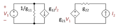 Two-port networkA two-port network is an electrical circuit or device with two pairs of terminals connected together internally by an electrical network...
s and find the only one with a CCCS is the g-parameter two-port, shown in Figure 4. The next task is to select the g-parameters so that the two-port of Figure 4 is electrically equivalent to the L-section made up of R2 and Rf. That selection is an algebraic procedure made most simply by looking at two individual cases: the case with V1 = 0, which makes the VCVS on the right side of the two-port a short-circuit; and the case with I2 = 0. which makes the CCCS on the left side an open circuit. The algebra in these two cases is simple, much easier than solving for all variables at once. The choice of g-parameters that make the two-port and the L-section behave the same way are shown in the table below.g11 g12 g21 g22 


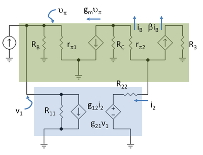
Small-signal circuit
The next step is to draw the small-signal schematic for the amplifier with the two-port in place using the hybrid-pi modelHybrid-pi modelThe hybrid-pi model is a popular circuit model used for analyzing the small signal behavior of bipolar junction and field effect transistors. The model can be quite accurate for low-frequency circuits and can easily be adapted for higher frequency circuits with the addition of appropriate...
for the transistors. Figure 5 shows the schematic with notation R3 = RC2 // RL and R11 = 1 / g11, R22 = g22 .
Loaded open-loop gain
Figure 3 indicates the output node, but not the choice of output variable. A useful choice is the short-circuit current output of the amplifier (leading to the short-circuit current gain). Because this variable leads simply to any of the other choices (for example, load voltage or load current), the short-circuit current gain is found below.
First the loaded open-loop gain is found. The feedback is turned off by setting g12 = g21 = 0. The idea is to find how much the amplifier gain is changed because of the resistors in the feedback network by themselves, with the feedback turned off. This calculation is pretty easy because R11, RB, and rπ1 all are in parallel and v1 = vπ. Let R1 = R11 // RB // rπ1. In addition, i2 = −(β+1) iB. The result for the open-loop current gain AOL is:
-

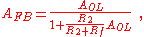
Gain with feedback
In the classical approach to feedback, the feedforward represented by the VCVS (that is, g21 v1) is neglected. That makes the circuit of Figure 5 resemble the block diagram of Figure 1, and the gain with feedback is then:
where the feedback factor βFB = −g12. Notation βFB is introduced for the feedback factor to distinguish it from the transistor β.
Input and output resistances
First, a digression on how two-port theory approaches resistance determination, and then its application to the amplifier at hand.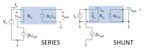
Background on resistance determination
Figure 6 shows an equivalent circuit for finding the input resistance of a feedback voltage amplifier (left) and for a feedback current amplifier (right). These arrangements are typical Miller theorem applications.
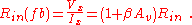
In the case of the voltage amplifier, the output voltage βVout of the feedback network is applied in series and with an opposite polarity to the input voltage Vx travelling over the loop (but in respect to ground, the polarities are the same). As a result, the effective voltage across and the current through the amplifier input resistance Rin decrease so that the circuit input resistance increases (one might say that Rin apparently increases). Its new value can be calculated by applying Miller theorem (for voltages) or the basic circuit laws. Thus Kirchhoff's voltage lawKirchhoff's circuit lawsKirchhoff's circuit laws are two equalities that deal with the conservation of charge and energy in electrical circuits, and were first described in 1845 by Gustav Kirchhoff...
provides:
where vout = Av vin = Av Ix Rin. Substituting this result in the above equation and solving for the input resistance of the feedback amplifier, the result is:
The general conclusion to be drawn from this example and a similar example for the output resistance case is:
A series feedback connection at the input (output) increases the input (output) resistance by a factor ( 1 + β AOL ), where AOL = open loop gain.
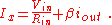
On the other hand, for the current amplifier, the output current βIout of the feedback network is applied in parallel and with an opposite direction to the input current Ix. As a result, the total current flowing through the circuit input (not only through the input resistance Rin) increases and the voltage across it decreases so that the circuit input resistance decreases (Rin apparently decreases). Its new value can be calculated by applying the dual Miller theorem (for currents) or the basic Kirchhoff's laws:
where iout = Ai iin = Ai Vx / Rin. Substituting this result in the above equation and solving for the input resistance of the feedback amplifier, the result is:
The general conclusion to be drawn from this example and a similar example for the output resistance case is:
A parallel feedback connection at the input (output) decreases the input (output) resistance by a factor ( 1 + β AOL ), where AOL = open loop gain.
These conclusions can be generalized to treat cases with arbitrary NortonNorton's theoremNorton's theorem for linear electrical networks, known in Europe as the Mayer–Norton theorem, states that any collection of voltage sources, current sources, and resistors with two terminals is electrically equivalent to an ideal current source, I, in parallel with a single resistor, R...
or ThéveninThévenin's theoremIn circuit theory, Thévenin's theorem for linear electrical networks states that any combination of voltage sources, current sources, and resistors with two terminals is electrically equivalent to a single voltage source V and a single series resistor R. For single frequency AC systems the theorem...
drives, arbitrary loads, and general two-port feedback networksTwo-port networkA two-port network is an electrical circuit or device with two pairs of terminals connected together internally by an electrical network...
. However, the results do depend upon the main amplifier having a representation as a two-port – that is, the results depend on the same current entering and leaving the input terminals, and likewise, the same current that leaves one output terminal must enter the other output terminal.
A broader conclusion to be drawn, independent of the quantitative details, is that feedback can be used to increase or to decrease the input and output impedances.
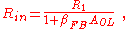
Application to the example amplifier
These resistance results now are applied to the amplifier of Figure 3 and Figure 5. The improvement factor that reduces the gain, namely ( 1 + βFB AOL), directly decides the effect of feedback upon the input and output resistances of the amplifier. In the case of a shunt connection, the input impedance is reduced by this factor; and in the case of series connection, the impedance is multiplied by this factor. However, the impedance that is modified by feedback is the impedance of the amplifier in Figure 5 with the feedback turned off, and does include the modifications to impedance caused by the resistors of the feedback network.
Therefore, the input impedance seen by the source with feedback turned off is Rin = R1 = R11 // RB // rπ1, and with the feedback turned on (but no feedforward)
where division is used because the input connection is shunt: the feedback two-port is in parallel with the signal source at the input side of the amplifier. A reminder: AOL is the loaded open loop gain found above, as modified by the resistors of the feedback network.
The impedance seen by the load needs further discussion. The load in Figure 5 is connected to the collector of the output transistor, and therefore is separated from the body of the amplifier by the infinite impedance of the output current source. Therefore, feedback has no effect on the output impedance, which remains simply RC2 as seen by the load resistor RL in Figure 3.
If instead we wanted to find the impedance presented at the emitter of the output transistor (instead of its collector), which is series connected to the feedback network, feedback would increase this resistance by the improvement factor ( 1 + βFB AOL).
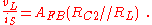
Load voltage and load current
The gain derived above is the current gain at the collector of the output transistor. To relate this gain to the gain when voltage is the output of the amplifier, notice that the output voltage at the load RL is related to the collector current by Ohm's lawOhm's lawOhm's law states that the current through a conductor between two points is directly proportional to the potential difference across the two points...
as vL = iC (RC2 // RL). Consequently, the transresistance gain vL / iS is found by multiplying the current gain by RC2 // RL:
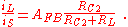
Similarly, if the output of the amplifier is taken to be the current in the load resistor RL, current division determines the load current, and the gain is then:
Is the main amplifier block a two port?
Some complications follow, intended for the attentive reader.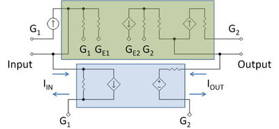
Figure 7 shows the small-signal schematic with the main amplifier and the feedback two-port in shaded boxes. The two-port satisfies the port conditionsTwo-port networkA two-port network is an electrical circuit or device with two pairs of terminals connected together internally by an electrical network...
: at the input port, Iin enters and leaves the port, and likewise at the output, Iout enters and leaves. The main amplifier is shown in the upper shaded box. The ground connections are labeled.
Figure 7 shows the interesting fact that the main amplifier does not satisfy the port conditions at its input and output unless the ground connections are chosen to make that happen. For example, on the input side, the current entering the main amplifier is IS. This current is divided three ways: to the feedback network, to the bias resistor RB and to the base resistance of the input transistor rπ. To satisfy the port condition for the main amplifier, all three components must be returned to the input side of the main amplifier, which means all the ground leads labeled G1 must be connected, as well as emitter lead GE1. Likewise, on the output side, all ground connections G2 must be connected and also ground connection GE2. Then, at the bottom of the schematic, underneath the feedback two-port and outside the amplifier blocks, G1 is connected to G2. That forces the ground currents to divide between the input and output sides as planned. Notice that this connection arrangement splits the emitter of the input transistor into a base-side and a collector-side – a physically impossible thing to do, but electrically the circuit sees all the ground connections as one node, so this fiction is permitted.
Of course, the way the ground leads are connected makes no difference to the amplifier (they are all one node), but it makes a difference to the port conditions. That is a weakness of this approach: the port conditions are needed to justify the method, but the circuit really is unaffected by how currents are traded among ground connections.
However, if there is no possible arrangement of ground conditions that will lead to the port conditions, the circuit might not behave the same way. The improvement factors ( 1 + βFB AOL) for determining input and output impedance might not work. This situation is awkward, because a failure to make a two-port may reflect a real problem (it just is not possible), or reflect a lack of imagination (for example, just did not think of splitting the emitter node in two). As a consequence, when the port conditions are in doubt, at least two approaches are possible to establish whether improvement factors are accurate: either simulate an example using SpiceSPICESPICE is a general-purpose, open source analog electronic circuit simulator.It is a powerful program that is used in integrated circuit and board-level design to check the integrity of circuit designs and to predict circuit behavior.- Introduction :Unlike board-level designs composed of discrete...
and compare results with use of an improvement factor, or calculate the impedance using a test source and compare results.
A more radical choice is to drop the two-port approach altogether, and use return ratioReturn ratioThe return ratio of a dependent source in a linear electrical circuit is the negative of the ratio of the current returned to the site of the dependent source to the current of a replacement independent source...
s. That choice might be advisable if small-signal device models are complex, or are not available (for example, the devices are known only numerically, perhaps from measurement or from SPICESPICESPICE is a general-purpose, open source analog electronic circuit simulator.It is a powerful program that is used in integrated circuit and board-level design to check the integrity of circuit designs and to predict circuit behavior.- Introduction :Unlike board-level designs composed of discrete...
simulations).
See also
- Asymptotic gain model
- Bode plotBode plotA Bode plot is a graph of the transfer function of a linear, time-invariant system versus frequency, plotted with a log-frequency axis, to show the system's frequency response...
- Buffer amplifier considers the basic op-amp amplifying stage with negative feedback
- Common collectorCommon collectorIn electronics, a common-collector amplifier is one of three basic single-stage bipolar junction transistor amplifier topologies, typically used as a voltage buffer...
(emitter follower) is dedicated to the basic transistor amplifying stage with negative feedback - Frequency compensationFrequency compensationIn electrical engineering, frequency compensation is a technique used in amplifiers, and especially in amplifiers employing negative feedback. It usually has two primary goals: To avoid the unintentional creation of positive feedback, which will cause the amplifier to oscillate, and to control...
- Miller theoremMiller theoremMiller theorem refers to the process of creating equivalent circuits. It asserts that a floating impedance element supplied by two voltage sources connected in series may be split into two grounded elements with corresponding impedances. There is also a dual Miller theorem with regards to impedance...
is a powerful tool for determining the input/output impedances of negative feedback circuits - Operational amplifierOperational amplifierAn operational amplifier is a DC-coupled high-gain electronic voltage amplifier with a differential input and, usually, a single-ended output...
presents the basic op-amp non-inverting amplifier and inverting amplifier - Operational amplifier applicationsOperational amplifier applicationsThis article illustrates some typical applications of operational amplifiers. A simplified schematic notation is used, and the reader is reminded that many details such as device selection and power supply connections are not shown....
shows the most typical op-amp circuits with negative feedback - Phase marginPhase marginIn electronic amplifiers, phase margin is the difference between the phase, measured in degrees, of an amplifier's output signal and 180°, as a function of frequency. The PM is taken as positive at frequencies below where the open-loop phase first crosses 180°, i.e. the signal becomes inverted,...
- Pole splittingPole splittingPole splitting is a phenomenon exploited in some forms of frequency compensation used in an electronic amplifier. When a capacitor is introduced between the input and output sides of the amplifier with the intention of moving the pole lowest in frequency to lower frequencies, pole splitting causes...
- Return ratioReturn ratioThe return ratio of a dependent source in a linear electrical circuit is the negative of the ratio of the current returned to the site of the dependent source to the current of a replacement independent source...
-
-
-
-