
Printed electronics
Encyclopedia
Printed electronics is a set of printing
methods used to create electrical devices on various substrates. Printing typically uses common printing equipment or other low-cost equipment suitable for defining patterns on material, such as screen printing, flexography
, gravure, offset lithography and inkjet. Electrically functional electronic or optical inks are deposited on the substrate, creating active or passive devices, such as thin film transistors or resistors. Printed electronics is expected to facilitate widespread, very low-cost, low-performance electronics for applications such as flexible displays, smart labels, decorative and animated posters, and active clothing that do not require high performance.
The term printed electronics is related to organic electronics
or plastic electronics, in which one or more inks are composed of carbon-based compounds. These other terms refer to the ink material, which can be deposited by solution-based, vacuum-based or some other method. Printed electronics, in contrast, specifies the process, and can utilize any solution-based material, including organic semiconductor
s, inorganic semiconductor
s, metallic conductors, nanoparticles, nanotubes
, etc.
For the preparation of printed electronics nearly all industrial printing methods are employed. Similar to conventional printing, printed electronics applies ink layers one atop another. so that the coherent development of printing methods and ink materials are the field's essential tasks.
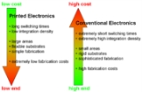
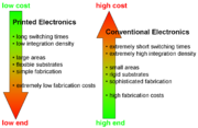
The most important benefit of printing is low-cost volume fabrication. The lower cost enables use in more applications. An example is RFID-systems, which enable contactless identification in trade and transport. In some domains, such as light-emitting diodes printing does not impact performance. Printing on flexible substrates allows electronics to be placed on curved surfaces, for example, putting solar cells on vehicle roofs. More typically, conventional semiconductors justify their much higher costs by providing much higher performance.
Control of thickness, holes, and material compatibility (wetting, adhesion, solvation) are essential, but matter in conventional printing only if the eye can detect them. Conversely, the visual impression is irrelevant.
Printing technologies divide between sheet-based and roll-to-roll-based approaches. Sheet-based techniques, such as inkjet and screen printing are best for low-volume, high-precision work. Gravure, offset
and flexographic printing
are more common for high-volume production, such as solar cells, reaching 10.000 square meters per hour (m²/h). While offset and flexographic printing are mainly used for inorganic and organic conductors (the latter also for dielectrics), gravure printing is especially suitable for quality-sensitive layers like organic semiconductors and semiconductor/dielectric-interfaces in transistors, due to high layer quality. In connection with high resolution, is also suitable for inorganic and organic conductors. Organic field-effect transistors and integrated circuit
s can be prepared completely by means of mass-printing methods.
Inkjets are flexible and versatile, and can be set up with relatively low effort. Inkjets are probably the most commonly used method. However, inkjets offer lower througput of around 100 m2/h and lower resolution (ca. 50 µm). It is well suited for low-viscosity
, soluble materials like organic semiconductors. With high-viscosity materials, like organic dielectrics, and dispersed particles, like inorganic metal inks, difficulties due to nozzle clogging occur. Because ink is deposited via droplets, thickness and dispersion homogeneity is reduced. Simultaneously using many nozzles and pre-structuring the substrate allows improvements in productivity and resolution, respectively. However, in the latter case non-printing methods must be employed for the actual patterning step. Inkjet printing is preferable for organic semiconductors in organic field-effect transistors
(OFETs) and organic light-emitting diode
s (OLEDs), but also OFETs completely prepared by this method have been demonstrated. Frontplanes and backplane
s of OLED-displays, integrated circuits, organic photovoltaic cells (OPVCs) and other devices can be prepared with inkjets.
Screen printing is appropriate for fabricating electrics and electronics on industrial scales due to its ability to produce thick layers from paste-like materials. This method can produce conducting lines from inorganic materials (e.g. for circuit boards and antennas), but also insulating and passivating layers, whereby layer thickness is more important than high resolution. Its 50 m²/h throughput and 100 µm resolution are similar to inkjets. This versatile and comparatively simple method is used mainly for conductive and dielectric layers, but also organic semiconductors, e.g. for OPVCs, and even complete OFETs can be printed.
Other methods with similarities to printing, among them micro-contact printing and nano-imprint lithography
are of interest. Here, µm- and nm-sized layers, respectively, are prepared by methods similar to stamping with soft and hard forms, respectively. Often the actual structures are prepared subtractively, e.g. by deposition of etch masks or by lift-off processes. For example electrodes for OFETs can be prepared Sporadically pad printing
is used in a similar manner. Occasionally so-called transfer methods, where solid layers are transferred from a carrier to the substrate, are considered printed electronics. Electrophotography
is currently not used in printed electronics.
Electronic functionality and printability can interfere with each other, mandating careful optimization. For example, a higher molecular weight in polymers enhances conductivity, but diminishes solubility. For printing, viscosity, surface tension and solid content must be tightly controlled. Cross-layer interactions such as wetting, adhesion, and solubility as well as post-deposition drying procedures affect the outcome. Additives often used in conventional printing inks are unavailable, because they often defeat electronic functionality.
Material properties largely determine the differences between printed and conventional electronics. Printable materials provide decisive advantages beside printability, such as mechanical flexibility and functional adjustment by chemical modification (e.g. light color in OLEDs).
Printed conductors offer lower conductivity and charge carrier mobility.
With a few exceptions, inorganic ink materials are dispersions of metallic micro- and nano-particles.
PMOS
but not CMOS
is possible in printed electronics.
The discovery of conjugated polymers
and their development into soluble materials provided the first organic ink materials. Materials from this class of polymers variously possess conducting, semiconducting
, electroluminescent
, photovoltaic
and other properties. Other polymers are used mostly as insulators and dielectrics.
In most organic materials, hole transport is favored over electron transport. Recent studies indicate that this is a specific feature of organic semiconductor/dielectric-interfaces, which play a major role in OFETs. Therefore p-type devices should dominate over n-type devices. Durability (resistance to dispersion) and lifetime is less than conventional materials.
Organic semiconductors include the conductive polymer
s poly(3,4-ethylene dioxitiophene), doped with poly(styrene sulfonate
), (PEDOT:PSS
) and poly(aniline
) (PANI). Both polymers are commercially available in different formulations and have been printed using inkjet, screen and offset printing or screen, flexo and gravure printing, respectively.
Polymer semiconductors are processed using inkjet printing, such as poly(thiopene)s
like poly(3-hexylthiophene) (P3HT) and poly(9,9-dioctylfluorene co-bithiophen) (F8T2). The latter material has also been gravure printed. Different electroluminescent polymers are used with inkjet printing, as well as active materials for photovoltaics (e.g. blends of P3HT with fullerene
derivatives), which in part also can be deposited using screen printing (e.g. blends of poly(phenylene vinylene)
with fullerene derivatives).
Printable organic and inorganic insulators and dielectrics exist, which can be processed with different printing methods.
Silver
nanoparticles are used with flexo, offset and inkjet. Gold
particles are used with inkjet.
A.C. electroluminescent (EL) multi-color displays can cover many tens of square meters, or be incorporated in watch faces and instrument displays. They involve six to eight printed inorganic layers, including a copper doped phosphor, on a plastic film substrate.
CIGS cells can be printed directly onto molybdenum
coated
glass sheets.
A printed gallium arsenide germanium solar cell demonstrated 40.7% conversion efficiency, eight times that of the best organic cells, approaching the best performance of heavy silicon.
-foil (PET) is a common choice, due to its low cost and higher temperature stability. Poly(ethylene naphthalate)
- (PEN) and poly(imide)
-foil (PI) are alternatives. Paper
's low costs and manifold applications make it an attractive substrate, however, its high roughness and large absorbency make it problematic for electronics.
Other important substrate criteria are low roughness and suitable wettability, which can be tuned pre-treatment (coating, corona
). In contrast to conventional printing, high absorbency is usually disadvantageous.
development (for sharing of product specifications, characterization standards, etc.) This strategy of standards development mirrors the approach used by silicon-based electronics over the past 50 years. Initiatives include:
Printing
Printing is a process for reproducing text and image, typically with ink on paper using a printing press. It is often carried out as a large-scale industrial process, and is an essential part of publishing and transaction printing....
methods used to create electrical devices on various substrates. Printing typically uses common printing equipment or other low-cost equipment suitable for defining patterns on material, such as screen printing, flexography
Flexography
Flexography is a form of printing process which utilizes a flexible relief plate. It is basically an updated version of letterpress that can be used for printing on almost any type of substrate including plastic, metallic films, cellophane, and paper...
, gravure, offset lithography and inkjet. Electrically functional electronic or optical inks are deposited on the substrate, creating active or passive devices, such as thin film transistors or resistors. Printed electronics is expected to facilitate widespread, very low-cost, low-performance electronics for applications such as flexible displays, smart labels, decorative and animated posters, and active clothing that do not require high performance.
The term printed electronics is related to organic electronics
Organic electronics
Organic electronics, plastic electronics or polymer electronics, is a branch of electronics dealing with conductive polymers, plastics, or small molecules. It is called 'organic' electronics because the polymers and small molecules are carbon-based...
or plastic electronics, in which one or more inks are composed of carbon-based compounds. These other terms refer to the ink material, which can be deposited by solution-based, vacuum-based or some other method. Printed electronics, in contrast, specifies the process, and can utilize any solution-based material, including organic semiconductor
Organic semiconductor
An organic semiconductor is an organic material with semiconductor properties. Single molecules, short chain and organic polymers can be semiconductive. Semiconducting small molecules include the polycyclic aromatic compounds pentacene, anthracene, and rubrene...
s, inorganic semiconductor
Semiconductor
A semiconductor is a material with electrical conductivity due to electron flow intermediate in magnitude between that of a conductor and an insulator. This means a conductivity roughly in the range of 103 to 10−8 siemens per centimeter...
s, metallic conductors, nanoparticles, nanotubes
Carbon nanotube
Carbon nanotubes are allotropes of carbon with a cylindrical nanostructure. Nanotubes have been constructed with length-to-diameter ratio of up to 132,000,000:1, significantly larger than for any other material...
, etc.
For the preparation of printed electronics nearly all industrial printing methods are employed. Similar to conventional printing, printed electronics applies ink layers one atop another. so that the coherent development of printing methods and ink materials are the field's essential tasks.
The most important benefit of printing is low-cost volume fabrication. The lower cost enables use in more applications. An example is RFID-systems, which enable contactless identification in trade and transport. In some domains, such as light-emitting diodes printing does not impact performance. Printing on flexible substrates allows electronics to be placed on curved surfaces, for example, putting solar cells on vehicle roofs. More typically, conventional semiconductors justify their much higher costs by providing much higher performance.
Resolution, registration, thickness, holes, materials
The maximum required resolution of structures in conventional printing is determined by the human eye. Feature sizes smaller than approximately 20 µm cannot be distinguished by the human eye and consequently exceed the capabilities of conventional printing processes. In contrast, higher resolution and smaller structures are necessary in electronics printing, because they directly affect circuit density and functionality (especially transistors). A similar requirement holds for the precision with which layers are printed on top of each other (layer to layer registration).Control of thickness, holes, and material compatibility (wetting, adhesion, solvation) are essential, but matter in conventional printing only if the eye can detect them. Conversely, the visual impression is irrelevant.
Printing technologies
The attraction of printing technology for the fabrication of electronics mainly results from the possibility to prepare stacks of micro-structured layers (and thereby thin-film devices) in a much more simple and cost-effective way compared to conventional electronics. Beside this, also the possibility to implement new or improved functionalities (e.g. mechanical flexibility) plays a role. The selection of used printing methods is determined by requirements concerning printed layers, by properties of printed materials as well as economic and technical considerations in terms of printed products.Printing technologies divide between sheet-based and roll-to-roll-based approaches. Sheet-based techniques, such as inkjet and screen printing are best for low-volume, high-precision work. Gravure, offset
Offset printing
Offset printing is a commonly used printing technique in which the inked image is transferred from a plate to a rubber blanket, then to the printing surface...
and flexographic printing
Flexography
Flexography is a form of printing process which utilizes a flexible relief plate. It is basically an updated version of letterpress that can be used for printing on almost any type of substrate including plastic, metallic films, cellophane, and paper...
are more common for high-volume production, such as solar cells, reaching 10.000 square meters per hour (m²/h). While offset and flexographic printing are mainly used for inorganic and organic conductors (the latter also for dielectrics), gravure printing is especially suitable for quality-sensitive layers like organic semiconductors and semiconductor/dielectric-interfaces in transistors, due to high layer quality. In connection with high resolution, is also suitable for inorganic and organic conductors. Organic field-effect transistors and integrated circuit
Integrated circuit
An integrated circuit or monolithic integrated circuit is an electronic circuit manufactured by the patterned diffusion of trace elements into the surface of a thin substrate of semiconductor material...
s can be prepared completely by means of mass-printing methods.
Inkjets are flexible and versatile, and can be set up with relatively low effort. Inkjets are probably the most commonly used method. However, inkjets offer lower througput of around 100 m2/h and lower resolution (ca. 50 µm). It is well suited for low-viscosity
Viscosity
Viscosity is a measure of the resistance of a fluid which is being deformed by either shear or tensile stress. In everyday terms , viscosity is "thickness" or "internal friction". Thus, water is "thin", having a lower viscosity, while honey is "thick", having a higher viscosity...
, soluble materials like organic semiconductors. With high-viscosity materials, like organic dielectrics, and dispersed particles, like inorganic metal inks, difficulties due to nozzle clogging occur. Because ink is deposited via droplets, thickness and dispersion homogeneity is reduced. Simultaneously using many nozzles and pre-structuring the substrate allows improvements in productivity and resolution, respectively. However, in the latter case non-printing methods must be employed for the actual patterning step. Inkjet printing is preferable for organic semiconductors in organic field-effect transistors
OFET
An organic field-effect transistor is a field effect transistor using an organic semiconductor in its channel. OFETs can be prepared either by vacuum evaporation of small molecules, by solution-casting of polymers or small molecules, or by mechanical transfer of a peeled single-crystalline organic...
(OFETs) and organic light-emitting diode
Organic light-emitting diode
An OLED is a light-emitting diode in which the emissive electroluminescent layer is a film of organic compounds which emit light in response to an electric current. This layer of organic semiconductor material is situated between two electrodes...
s (OLEDs), but also OFETs completely prepared by this method have been demonstrated. Frontplanes and backplane
Backplane
A backplane is a group of connectors connected in parallel with each other, so that each pin of each connector is linked to the same relative pin of all the other connectors forming a computer bus. It is used as a backbone to connect several printed circuit boards together to make up a complete...
s of OLED-displays, integrated circuits, organic photovoltaic cells (OPVCs) and other devices can be prepared with inkjets.
Screen printing is appropriate for fabricating electrics and electronics on industrial scales due to its ability to produce thick layers from paste-like materials. This method can produce conducting lines from inorganic materials (e.g. for circuit boards and antennas), but also insulating and passivating layers, whereby layer thickness is more important than high resolution. Its 50 m²/h throughput and 100 µm resolution are similar to inkjets. This versatile and comparatively simple method is used mainly for conductive and dielectric layers, but also organic semiconductors, e.g. for OPVCs, and even complete OFETs can be printed.
Other methods with similarities to printing, among them micro-contact printing and nano-imprint lithography
Nanoimprint Lithography
Nanoimprint lithography is a method of fabricating nanometer scale patterns. It is a simple nanolithography process with low cost, high throughput and high resolution. It creates patterns by mechanical deformation of imprint resist and subsequent processes. The imprint resist is typically a monomer...
are of interest. Here, µm- and nm-sized layers, respectively, are prepared by methods similar to stamping with soft and hard forms, respectively. Often the actual structures are prepared subtractively, e.g. by deposition of etch masks or by lift-off processes. For example electrodes for OFETs can be prepared Sporadically pad printing
Pad printing
Pad printing is a printing process that can transfer a 2-D image onto a 3-D object. This is accomplished using an indirect offset printing process that involves an image being transferred from the cliché via a silicone pad onto a substrate...
is used in a similar manner. Occasionally so-called transfer methods, where solid layers are transferred from a carrier to the substrate, are considered printed electronics. Electrophotography
Xerography
Xerography is a dry photocopying technique invented by Chester Carlson in 1938, for which he was awarded on October 6, 1942. Carlson originally called his invention electrophotography...
is currently not used in printed electronics.
Materials
Both organic and inorganic materials are used for printed electronics. Ink materials must be available in liquid form, for solution, dispersion or suspension. They must function as conductors, semiconductors, dielectrics, or insulators. Material costs must be fit the application.Electronic functionality and printability can interfere with each other, mandating careful optimization. For example, a higher molecular weight in polymers enhances conductivity, but diminishes solubility. For printing, viscosity, surface tension and solid content must be tightly controlled. Cross-layer interactions such as wetting, adhesion, and solubility as well as post-deposition drying procedures affect the outcome. Additives often used in conventional printing inks are unavailable, because they often defeat electronic functionality.
Material properties largely determine the differences between printed and conventional electronics. Printable materials provide decisive advantages beside printability, such as mechanical flexibility and functional adjustment by chemical modification (e.g. light color in OLEDs).
Printed conductors offer lower conductivity and charge carrier mobility.
With a few exceptions, inorganic ink materials are dispersions of metallic micro- and nano-particles.
PMOS
PMOS logic
P-type metal-oxide-semiconductor logic uses p-type metal-oxide-semiconductor field effect transistors to implement logic gates and other digital circuits...
but not CMOS
CMOS
Complementary metal–oxide–semiconductor is a technology for constructing integrated circuits. CMOS technology is used in microprocessors, microcontrollers, static RAM, and other digital logic circuits...
is possible in printed electronics.
Organic materials
Organic printed electronics integrates knowledge and developments from printing, electronics, chemistry, and materials science, especially from organic and polymer chemistry. Organic materials in part differ from conventional electronics in terms of structure, operation and functionality, which influences device and circuit design and optimization as well as fabrication method.The discovery of conjugated polymers
Conductive polymer
Conductive polymers or, more precisely, intrinsically conducting polymers are organic polymers that conduct electricity. Such compounds may have metallic conductivity or can be semiconductors. The biggest advantage of conductive polymers is their processability, mainly by dispersion. Conductive...
and their development into soluble materials provided the first organic ink materials. Materials from this class of polymers variously possess conducting, semiconducting
Semiconductor
A semiconductor is a material with electrical conductivity due to electron flow intermediate in magnitude between that of a conductor and an insulator. This means a conductivity roughly in the range of 103 to 10−8 siemens per centimeter...
, electroluminescent
Electroluminescence
Electroluminescence is an optical phenomenon and electrical phenomenon in which a material emits light in response to the passage of an electric current or to a strong electric field...
, photovoltaic
Photovoltaics
Photovoltaics is a method of generating electrical power by converting solar radiation into direct current electricity using semiconductors that exhibit the photovoltaic effect. Photovoltaic power generation employs solar panels composed of a number of solar cells containing a photovoltaic material...
and other properties. Other polymers are used mostly as insulators and dielectrics.
In most organic materials, hole transport is favored over electron transport. Recent studies indicate that this is a specific feature of organic semiconductor/dielectric-interfaces, which play a major role in OFETs. Therefore p-type devices should dominate over n-type devices. Durability (resistance to dispersion) and lifetime is less than conventional materials.
Organic semiconductors include the conductive polymer
Polymer
A polymer is a large molecule composed of repeating structural units. These subunits are typically connected by covalent chemical bonds...
s poly(3,4-ethylene dioxitiophene), doped with poly(styrene sulfonate
Sulfonate
A sulfonate is a salt or ester of a sulfonic acid. It contains the functional group R-SO2O-.- Sulfonate salts:Anions with the general formula RSO2O− are called sulfonates. They are the conjugate bases of sulfonic acids with formula RSO2OH. As sulfonic acids tend to be strong acids, the...
), (PEDOT:PSS
PEDOT:PSS
PEDOT:PSS or Poly poly is a polymer mixture of two ionomers. One component in this mixture is made up of sodium polystyrene sulfonate which is a sulfonated polystyrene. Part of the sulfonyl groups are deprotonated and carry a negative charge...
) and poly(aniline
Aniline
Aniline, phenylamine or aminobenzene is an organic compound with the formula C6H5NH2. Consisting of a phenyl group attached to an amino group, aniline is the prototypical aromatic amine. Being a precursor to many industrial chemicals, its main use is in the manufacture of precursors to polyurethane...
) (PANI). Both polymers are commercially available in different formulations and have been printed using inkjet, screen and offset printing or screen, flexo and gravure printing, respectively.
Polymer semiconductors are processed using inkjet printing, such as poly(thiopene)s
Polythiophene
Polythiophenes result from the polymerization of thiophenes, a sulfur heterocycle, that can become conducting when electrons are added or removed from the conjugated π-orbitals via doping....
like poly(3-hexylthiophene) (P3HT) and poly(9,9-dioctylfluorene co-bithiophen) (F8T2). The latter material has also been gravure printed. Different electroluminescent polymers are used with inkjet printing, as well as active materials for photovoltaics (e.g. blends of P3HT with fullerene
Fullerene
A fullerene is any molecule composed entirely of carbon, in the form of a hollow sphere, ellipsoid, or tube. Spherical fullerenes are also called buckyballs, and they resemble the balls used in association football. Cylindrical ones are called carbon nanotubes or buckytubes...
derivatives), which in part also can be deposited using screen printing (e.g. blends of poly(phenylene vinylene)
Poly(p-phenylene vinylene)
Poly is a conducting polymer of the rigid-rod polymer host family.PPV is the only polymer of this type that has so far been successfully processed into a highly ordered crystalline thin film. PPV and its derivatives are conducting polymers of rigid-rod polymer family...
with fullerene derivatives).
Printable organic and inorganic insulators and dielectrics exist, which can be processed with different printing methods.
Inorganic materials
Inorganic electronics provides highly ordered layers and interfaces that organic and polymer materials cannot provide.Silver
Silver
Silver is a metallic chemical element with the chemical symbol Ag and atomic number 47. A soft, white, lustrous transition metal, it has the highest electrical conductivity of any element and the highest thermal conductivity of any metal...
nanoparticles are used with flexo, offset and inkjet. Gold
Gold
Gold is a chemical element with the symbol Au and an atomic number of 79. Gold is a dense, soft, shiny, malleable and ductile metal. Pure gold has a bright yellow color and luster traditionally considered attractive, which it maintains without oxidizing in air or water. Chemically, gold is a...
particles are used with inkjet.
A.C. electroluminescent (EL) multi-color displays can cover many tens of square meters, or be incorporated in watch faces and instrument displays. They involve six to eight printed inorganic layers, including a copper doped phosphor, on a plastic film substrate.
CIGS cells can be printed directly onto molybdenum
Molybdenum
Molybdenum , is a Group 6 chemical element with the symbol Mo and atomic number 42. The name is from Neo-Latin Molybdaenum, from Ancient Greek , meaning lead, itself proposed as a loanword from Anatolian Luvian and Lydian languages, since its ores were confused with lead ores...
coated
Coating
Coating is a covering that is applied to the surface of an object, usually referred to as the substrate. In many cases coatings are applied to improve surface properties of the substrate, such as appearance, adhesion, wetability, corrosion resistance, wear resistance, and scratch resistance...
glass sheets.
A printed gallium arsenide germanium solar cell demonstrated 40.7% conversion efficiency, eight times that of the best organic cells, approaching the best performance of heavy silicon.
Substrates
Printed electronics allows the use of flexible substrates, which lowers production costs and allows fabrication of mechanically flexible circuits. While inkjet and screen printing typically imprint rigid substrates like glass and silicon, mass-printing methods nearly exclusively use flexible foil and paper. Poly(ethylene terephthalate)Polyethylene terephthalate
Polyethylene terephthalate , commonly abbreviated PET, PETE, or the obsolete PETP or PET-P, is a thermoplastic polymer resin of the polyester family and is used in synthetic fibers; beverage, food and other liquid containers; thermoforming applications; and engineering resins often in combination...
-foil (PET) is a common choice, due to its low cost and higher temperature stability. Poly(ethylene naphthalate)
Polyethylene naphthalate
Polyethylene naphthalate Polyethylene naphthalate (PEN) Polyethylene naphthalate (PEN) (Poly(ethylene 2,6-naphthalate) is a polyester with good barrier properties (even better than Polyethylene terephthalate). Because it provides a very good oxygen barrier, it is particularly well-suited for...
- (PEN) and poly(imide)
Polyimide
Polyimide is a polymer of imide monomers. The structure of imide is as shown. Polyimides have been in mass production since 1955...
-foil (PI) are alternatives. Paper
Paper
Paper is a thin material mainly used for writing upon, printing upon, drawing or for packaging. It is produced by pressing together moist fibers, typically cellulose pulp derived from wood, rags or grasses, and drying them into flexible sheets....
's low costs and manifold applications make it an attractive substrate, however, its high roughness and large absorbency make it problematic for electronics.
Other important substrate criteria are low roughness and suitable wettability, which can be tuned pre-treatment (coating, corona
Corona poling
Corona discharge is a partial breakdown of air, usually at atmospheric pressure, and is initiated by a discharge in an inhomogeneous electric field . Corona discharge has been used to pole films of electro-optic materials to enhance their electro-optic properties. Although corona poling can be...
). In contrast to conventional printing, high absorbency is usually disadvantageous.
Applications
Printed electronics are in use or under consideration for:- Radio frequency identificationRadio Frequency IdentificationRadio-frequency identification is a technology that uses radio waves to transfer data from an electronic tag, called RFID tag or label, attached to an object, through a reader for the purpose of identifying and tracking the object. Some RFID tags can be read from several meters away and beyond the...
(RFID) tags - Monitoring
- Data storage
- Display and visual effects
- Toys
Standards development and activities
Technical standards and roadmapping initiatives are intended to facilitate value chainValue chain
The value chain, is a concept from business management that was first described and popularized by Michael Porter in his 1985 best-seller, Competitive Advantage: Creating and Sustaining Superior Performance.-Firm Level:...
development (for sharing of product specifications, characterization standards, etc.) This strategy of standards development mirrors the approach used by silicon-based electronics over the past 50 years. Initiatives include:
- The IEEE Standards AssociationIEEE Standards AssociationThe Institute of Electrical and Electronics Engineers Standards Association is an organization within IEEE that develops global standards in a broad range of industries, including: power and energy, biomedical and health care, information technology, telecommunication, transportation,...
has published IEEE 1620-2004 and IEEE 1620.1-2006. - Similar to the well-established International Technology Roadmap for SemiconductorsInternational Technology Roadmap for SemiconductorsThe International Technology Roadmap for Semiconductors is a set of documents produced by a group of semiconductor industry experts. These experts are representative of the sponsoring organisations which include the Semiconductor Industry Associations of the US, Europe, Japan, South Korea and...
(ITRS), the International Electronics Manufacturing Initiative (iNEMI) has published a roadmap for printed and other organic electronicsOrganic electronicsOrganic electronics, plastic electronics or polymer electronics, is a branch of electronics dealing with conductive polymers, plastics, or small molecules. It is called 'organic' electronics because the polymers and small molecules are carbon-based...
.
External links
- For a history of the field, see Printed Organic and Molecular Electronics, edited by D. Gamota, P. Brazis, K. Kalyanasundaram, and J. Zhang (Kluwer Academic Publishers: New York, 2004). ISBN 1-4020-7707-6
- Cleaner Electronics Research Group - Brunel University
- Encyclopedia of Printed Electronics (IDTechEx)
- Printed Electronics conference/exhibition Asia USA
- Come Back Inorganic Electronics - All Is Forgiven
- New Nano Silver Powder Enables Flexible Printed Circuits (Ferro CorporationFerro CorporationFerro Corporation , is a leading global producer of technology-based performance materials for manufacturers and is headquartered in Cleveland, Ohio. In 2007, the company was listed as 844 on the Fortune 1000....
) - Western Michigan University's Center for Advancement of Printed Electronics (CAPE) includes AccuPress gravure printer
- Major Trends in Gravure Printed Electronics June 2010