

Local oxidation nanolithography
Encyclopedia
Scanning probe lithography
Scanning probe lithography describe a set of lithographic methods, in which a microscopic or nanoscopic stylus is moved mechanically across a surface to form a pattern.This type of method can be split in two different groups:...
nanofabrication method. It is based on the spatial confinement on an oxidation
Redox
Redox reactions describe all chemical reactions in which atoms have their oxidation state changed....
reaction under the sharp tip of an atomic force microscope
Atomic force microscope
Atomic force microscopy or scanning force microscopy is a very high-resolution type of scanning probe microscopy, with demonstrated resolution on the order of fractions of a nanometer, more than 1000 times better than the optical diffraction limit...
.
The first materials on which LON was demonstrated were Si
Silicon
Silicon is a chemical element with the symbol Si and atomic number 14. A tetravalent metalloid, it is less reactive than its chemical analog carbon, the nonmetal directly above it in the periodic table, but more reactive than germanium, the metalloid directly below it in the table...
(111) and polycrystalline tantalum
Tantalum
Tantalum is a chemical element with the symbol Ta and atomic number 73. Previously known as tantalium, the name comes from Tantalus, a character in Greek mythology. Tantalum is a rare, hard, blue-gray, lustrous transition metal that is highly corrosion resistant. It is part of the refractory...
. Subsequently, the technique has been extended to III
Boron group
The boron group is the series of elements in group 13 of the periodic table, comprising boron , aluminium , gallium , indium , thallium , and ununtrium . The elements in the boron group are characterized by having three electrons in their outer energy levels...
–V
Nitrogen group
The nitrogen group is a periodic table group consisting of nitrogen , phosphorus , arsenic , antimony , bismuth and ununpentium ....
semiconductor
Semiconductor
A semiconductor is a material with electrical conductivity due to electron flow intermediate in magnitude between that of a conductor and an insulator. This means a conductivity roughly in the range of 103 to 10−8 siemens per centimeter...
s, silicon carbide
Silicon carbide
Silicon carbide , also known as carborundum, is a compound of silicon and carbon with chemical formula SiC. It occurs in nature as the extremely rare mineral moissanite. Silicon carbide powder has been mass-produced since 1893 for use as an abrasive...
, metal
Metal
A metal , is an element, compound, or alloy that is a good conductor of both electricity and heat. Metals are usually malleable and shiny, that is they reflect most of incident light...
s such as titanium
Titanium
Titanium is a chemical element with the symbol Ti and atomic number 22. It has a low density and is a strong, lustrous, corrosion-resistant transition metal with a silver color....
, tantalum, aluminium
Aluminium
Aluminium or aluminum is a silvery white member of the boron group of chemical elements. It has the symbol Al, and its atomic number is 13. It is not soluble in water under normal circumstances....
, molybdenum
Molybdenum
Molybdenum , is a Group 6 chemical element with the symbol Mo and atomic number 42. The name is from Neo-Latin Molybdaenum, from Ancient Greek , meaning lead, itself proposed as a loanword from Anatolian Luvian and Lydian languages, since its ores were confused with lead ores...
, nickel
Nickel
Nickel is a chemical element with the chemical symbol Ni and atomic number 28. It is a silvery-white lustrous metal with a slight golden tinge. Nickel belongs to the transition metals and is hard and ductile...
and niobium
Niobium
Niobium or columbium , is a chemical element with the symbol Nb and atomic number 41. It's a soft, grey, ductile transition metal, which is often found in the pyrochlore mineral, the main commercial source for niobium, and columbite...
; thin films of manganite
Manganite
Manganite is a mineral. Its composition is manganese oxide-hydroxide, MnO, crystallizing in the monoclinic system . Crystals of manganite are prismatic and deeply striated parallel to their length; they are often grouped together in bundles. The color is dark steel-grey to iron-black, and the...
in the perovskite
Perovskite
A perovskite structure is any material with the same type of crystal structure as calcium titanium oxide , known as the perovskite structure, or XIIA2+VIB4+X2−3 with the oxygen in the face centers. Perovskites take their name from this compound, which was first discovered in the Ural mountains of...
form; dielectric
Dielectric
A dielectric is an electrical insulator that can be polarized by an applied electric field. When a dielectric is placed in an electric field, electric charges do not flow through the material, as in a conductor, but only slightly shift from their average equilibrium positions causing dielectric...
s like silicon nitride
Silicon nitride
Silicon nitride is a chemical compound of silicon and nitrogen. If powdered silicon is heated between 1300° and 1400°C in an atmosphere of nitrogen, trisilicon tetranitride, Si3N4, is formed. The silicon sample weight increases progressively due to the chemical combination of silicon and nitrogen...
, organosilane self-assembled monolayer
Self-assembled monolayer
A self assembled monolayer is an organized layer of amphiphilic molecules in which one end of the molecule, the “head group” shows a specific, reversible affinity for a substrate...
s, dendritic
Dendrite (crystal)
A crystal dendrite is a crystal that develops with a typical multi-branching tree-like form. Dendritic crystal growth is very common and illustrated by snowflake formation and frost patterns on a window. Dendritic crystallization forms a natural fractal pattern...
macromolecules and carbon
Carbon
Carbon is the chemical element with symbol C and atomic number 6. As a member of group 14 on the periodic table, it is nonmetallic and tetravalent—making four electrons available to form covalent chemical bonds...
aceous films.
History
The local oxidation of a surface by means of a scanning probe technique was first observed by Dagata and co-workers in 1990 who locally modified a hydrogenHydrogen
Hydrogen is the chemical element with atomic number 1. It is represented by the symbol H. With an average atomic weight of , hydrogen is the lightest and most abundant chemical element, constituting roughly 75% of the Universe's chemical elemental mass. Stars in the main sequence are mainly...
-terminated silicon
Silicon
Silicon is a chemical element with the symbol Si and atomic number 14. A tetravalent metalloid, it is less reactive than its chemical analog carbon, the nonmetal directly above it in the periodic table, but more reactive than germanium, the metalloid directly below it in the table...
surface into silicon dioxide
Silicon dioxide
The chemical compound silicon dioxide, also known as silica , is an oxide of silicon with the chemical formula '. It has been known for its hardness since antiquity...
by applying a bias voltage between the tip of a scanning tunneling microscope
Scanning tunneling microscope
A scanning tunneling microscope is an instrument for imaging surfaces at the atomic level. Its development in 1981 earned its inventors, Gerd Binnig and Heinrich Rohrer , the Nobel Prize in Physics in 1986. For an STM, good resolution is considered to be 0.1 nm lateral resolution and...
and the surface itself. In 1993 Day and Allee demonstrated the possibility of performing local oxidation experiments with an atomic force microscope
Atomic force microscope
Atomic force microscopy or scanning force microscopy is a very high-resolution type of scanning probe microscopy, with demonstrated resolution on the order of fractions of a nanometer, more than 1000 times better than the optical diffraction limit...
, which opened the way to applying the technique to a large variety of materials.
Basic principle
Atomic force microscope
Atomic force microscopy or scanning force microscopy is a very high-resolution type of scanning probe microscopy, with demonstrated resolution on the order of fractions of a nanometer, more than 1000 times better than the optical diffraction limit...
operated in contact or noncontact mode with additional circuits to apply voltage
Voltage
Voltage, otherwise known as electrical potential difference or electric tension is the difference in electric potential between two points — or the difference in electric potential energy per unit charge between two points...
pulses between tip and sample. The local oxidation process is mediated by the formation of a water meniscus
Meniscus
The meniscus is the curve in the upper surface of a liquid close to the surface of the container or another object, caused by surface tension. It can be either convex or concave. A convex meniscus occurs when the molecules have a stronger attraction to each other than to the material of the...
.
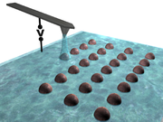
In order to perform Local Oxidation Nanolithography, the relative humidity
Relative humidity
Relative humidity is a term used to describe the amount of water vapor in a mixture of air and water vapor. It is defined as the partial pressure of water vapor in the air-water mixture, given as a percentage of the saturated vapor pressure under those conditions...
in the AFM chamber is kept between 30% and 60%. A voltage pulse is applied between a conductive AFM tip and the sample. The applied voltage induces the formation of a water bridge between tip and sample whenever the amplitude of the voltage pulse is above a certain threshold voltage. When the liquid meniscus
Meniscus
The meniscus is the curve in the upper surface of a liquid close to the surface of the container or another object, caused by surface tension. It can be either convex or concave. A convex meniscus occurs when the molecules have a stronger attraction to each other than to the material of the...
is created the applied voltage pulse causes an oxidation
Electrolytic cell
An electrolytic cell decomposes chemical compounds by means of electrical energy, in a process called electrolysis; the Greek word lysis means to break up. The result is that the chemical energy is increased...
reaction by breaking the covalent bond
Covalent bond
A covalent bond is a form of chemical bonding that is characterized by the sharing of pairs of electrons between atoms. The stable balance of attractive and repulsive forces between atoms when they share electrons is known as covalent bonding....
s in the water molecule
Molecule
A molecule is an electrically neutral group of at least two atoms held together by covalent chemical bonds. Molecules are distinguished from ions by their electrical charge...
s. The liquid bridge provides the oxyanion
Oxyanion
An oxyanion or oxoanion is a chemical compound with the generic formula AxOyz− . Oxoanions are formed by a large majority of the chemical elements. The formulae of simple oxoanions are determined by the octet rule...
s (OH-
Hydroxyl
A hydroxyl is a chemical group containing an oxygen atom covalently bonded with a hydrogen atom. In inorganic chemistry, the hydroxyl group is known as the hydroxide ion, and scientists and reference works generally use these different terms though they refer to the same chemical structure in...
,O-) needed to form the oxide and confines the lateral extension of the region to be oxidized.
The chemical reactions that govern the Local Oxidation in a metal
Metal
A metal , is an element, compound, or alloy that is a good conductor of both electricity and heat. Metals are usually malleable and shiny, that is they reflect most of incident light...
lic substrate (M) are the following:


while hydrogen
Hydrogen
Hydrogen is the chemical element with atomic number 1. It is represented by the symbol H. With an average atomic weight of , hydrogen is the lightest and most abundant chemical element, constituting roughly 75% of the Universe's chemical elemental mass. Stars in the main sequence are mainly...
gas is liberated at the AFM tip through the reduction reaction:

When the voltage pulse is off the AFM feedback forces the cantilever
Cantilever
A cantilever is a beam anchored at only one end. The beam carries the load to the support where it is resisted by moment and shear stress. Cantilever construction allows for overhanging structures without external bracing. Cantilevers can also be constructed with trusses or slabs.This is in...
to recover its original oscillation amplitude withdrawing the tip from the sample and breaking the liquid meniscus. Finally the AFM continues to scan the sample thus allowing to image MOn nanostructure fabricated during the Local Oxidation process with the very same tip used for its fabrication.
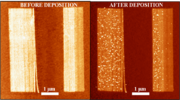
The method to form liquid bridges is so precise that water meniscus diameters of 20 nm or below are easily obtained. This has led to the reproducible fabrication of sub-10 nm structures in silicon and other metallic surfaces.
Experimental setup
Local oxidation experiments can be performed with almost any kind of atomic force microscopeAtomic force microscope
Atomic force microscopy or scanning force microscopy is a very high-resolution type of scanning probe microscopy, with demonstrated resolution on the order of fractions of a nanometer, more than 1000 times better than the optical diffraction limit...
. The key requirement is the possibility to apply voltage
Voltage
Voltage, otherwise known as electrical potential difference or electric tension is the difference in electric potential between two points — or the difference in electric potential energy per unit charge between two points...
pulses between the tip and the sample. It is recommendable to enclose the microscope in a chamber where the atmosphere is controlled. In the simplest case, the oxidant
Oxidizing agent
An oxidizing agent can be defined as a substance that removes electrons from another reactant in a redox chemical reaction...
is water vapor
Water vapor
Water vapor or water vapour , also aqueous vapor, is the gas phase of water. It is one state of water within the hydrosphere. Water vapor can be produced from the evaporation or boiling of liquid water or from the sublimation of ice. Under typical atmospheric conditions, water vapor is continuously...
, which is naturally present in the air. Controlling the relative humidity
Relative humidity
Relative humidity is a term used to describe the amount of water vapor in a mixture of air and water vapor. It is defined as the partial pressure of water vapor in the air-water mixture, given as a percentage of the saturated vapor pressure under those conditions...
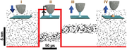
generally helps to obtain more reproducible results. The size of the fabricated features depends on a number of parameters, such as the distance between the sample and the tip, the amplitude and the duration of the voltage pulse, and the relative humidity of the atmosphere.
Applications

Nanolithography
Nanolithography is the branch of nanotechnology concerned with the study and application of fabricating nanometer-scale structures, meaning patterns with at least one lateral dimension between the size of an individual atom and approximately 100 nm...
is the focus of an intense research activity because progress on nanotechnology
Nanotechnology
Nanotechnology is the study of manipulating matter on an atomic and molecular scale. Generally, nanotechnology deals with developing materials, devices, or other structures possessing at least one dimension sized from 1 to 100 nanometres...
depends on the capability to fabricate, position and interconnect nanometer-scale structures.
Patterning
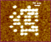
Local Oxidation Nanolithography allows to create a large variety of motives like dots, lines and letters with nanometer accuracy. In 2005, researchers at the Spanish National Research Council in MadridMadrid
Madrid is the capital and largest city of Spain. The population of the city is roughly 3.3 million and the entire population of the Madrid metropolitan area is calculated to be 6.271 million. It is the third largest city in the European Union, after London and Berlin, and its metropolitan...
wrote the first ten lines of Cervantes'
Miguel de Cervantes
Miguel de Cervantes Saavedra was a Spanish novelist, poet, and playwright. His magnum opus, Don Quixote, considered the first modern novel, is a classic of Western literature, and is regarded amongst the best works of fiction ever written...
Don Quixote on a few square micrometres of silicon. This pattern versatility can be used for information storage
Data storage device
thumb|200px|right|A reel-to-reel tape recorder .The magnetic tape is a data storage medium. The recorder is data storage equipment using a portable medium to store the data....
or to design etch-resistant nanomasks
Photomask
A photomask is an opaque plate with holes or transparencies that allow light to shine through in a defined pattern. They are commonly used in photolithography.-Overview:...
in order to fabricate nanodevices
Nanocircuitry
Nanocircuits are electrical circuits operating on the nanometer scale. This is well into the quantum realm, where quantum mechanical effects become very important. One nanometer is equal to 10-9 meters or a row of 10 hydrogen atoms. With such progressively smaller circuits, more can be fitted on...
as well as many other applications.
Data storage
Binary code
A binary code is a way of representing text or computer processor instructions by the use of the binary number system's two-binary digits 0 and 1. This is accomplished by assigning a bit string to each particular symbol or instruction...
considering the presence of a nanostructure as a 1 and its lack as a 0. In this way information can be stored in a small surface with a single SiO2
Silicon dioxide
The chemical compound silicon dioxide, also known as silica , is an oxide of silicon with the chemical formula '. It has been known for its hardness since antiquity...
dot constituting a bit
Bit
A bit is the basic unit of information in computing and telecommunications; it is the amount of information stored by a digital device or other physical system that exists in one of two possible distinct states...
. In 1999 Cooper et al. demonstrated that this methods allows to obtain an information density of 1.6 Tbit
Terabit
The terabit is a multiple of the unit bit for digital information or computer storage. The prefix tera is defined in the International System of Units as a multiplier of 1012 , and therefore...
/in2. However, only read-only memories
Read-only memory
Read-only memory is a class of storage medium used in computers and other electronic devices. Data stored in ROM cannot be modified, or can be modified only slowly or with difficulty, so it is mainly used to distribute firmware .In its strictest sense, ROM refers only...
can be fabricated with this technique.
Molecular template growth and preferencial deposition
Molecule
A molecule is an electrically neutral group of at least two atoms held together by covalent chemical bonds. Molecules are distinguished from ions by their electrical charge...
s like single molecule magnets, biomolecule
Biomolecule
A biomolecule is any molecule that is produced by a living organism, including large polymeric molecules such as proteins, polysaccharides, lipids, and nucleic acids as well as small molecules such as primary metabolites, secondary metabolites, and natural products...
s and conjugated organic molecules
Conjugated system
In chemistry, a conjugated system is a system of connected p-orbitals with delocalized electrons in compounds with alternating single and multiple bonds, which in general may lower the overall energy of the molecule and increase stability. Lone pairs, radicals or carbenium ions may be part of the...
.
This method of nanopositioning is an important tool for the fabrication of new nanodevices based on the novel properties exhibited by some nanoparticle
Nanoparticle
In nanotechnology, a particle is defined as a small object that behaves as a whole unit in terms of its transport and properties. Particles are further classified according to size : in terms of diameter, coarse particles cover a range between 10,000 and 2,500 nanometers. Fine particles are sized...
s and molecules. Potential applications of single-molecule magnets (SMMs) such as Mn12 as bits for information storage or qubit
Qubit
In quantum computing, a qubit or quantum bit is a unit of quantum information—the quantum analogue of the classical bit—with additional dimensions associated to the quantum properties of a physical atom....
s for quantum computation
Quantum computer
A quantum computer is a device for computation that makes direct use of quantum mechanical phenomena, such as superposition and entanglement, to perform operations on data. Quantum computers are different from traditional computers based on transistors...
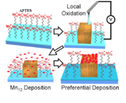
require methods for nanoscale-controlled positioning and/or manipulation of those molecules. The patterning of the Mn12 molecules on a silicon surface is achieved by first derivatizing this surface with a self-assembled monolayer
Self-assembled monolayer
A self assembled monolayer is an organized layer of amphiphilic molecules in which one end of the molecule, the “head group” shows a specific, reversible affinity for a substrate...
of APTES, which leaves it terminated by amino
Amine
Amines are organic compounds and functional groups that contain a basic nitrogen atom with a lone pair. Amines are derivatives of ammonia, wherein one or more hydrogen atoms have been replaced by a substituent such as an alkyl or aryl group. Important amines include amino acids, biogenic amines,...
groups (-NH2). Such termination electrostatically repels the Mn12 molecules. Subsequently, a pattern of silicon dioxide is defined by LON. The SMM molecules are predominantly deposited on the oxide motives because of electrostatic attraction. The electrostatic attraction between the silicon oxide fabricated by LON and the Mn12 molecules achieves the preferential deposition of this molecules with a nanoscale accuracy.
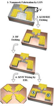
Fabrication of nanodevices
SQUID
A SQUID is a very sensitive magnetometer used to measure extremely weak magnetic fields, based on superconducting loops containing Josephson junctions....
s. LON also allows to fabricate silicon
Silicon
Silicon is a chemical element with the symbol Si and atomic number 14. A tetravalent metalloid, it is less reactive than its chemical analog carbon, the nonmetal directly above it in the periodic table, but more reactive than germanium, the metalloid directly below it in the table...
nanowire
Nanowire
A nanowire is a nanostructure, with the diameter of the order of a nanometer . Alternatively, nanowires can be defined as structures that have a thickness or diameter constrained to tens of nanometers or less and an unconstrained length. At these scales, quantum mechanical effects are important —...
s (SiNWs) in a top-down fashion starting from silicon on insulator
Silicon on insulator
Silicon on insulator technology refers to the use of a layered silicon-insulator-silicon substrate in place of conventional silicon substrates in semiconductor manufacturing, especially microelectronics, to reduce parasitic device capacitance and thereby improving performance...
(SOI) wafers
Wafer (electronics)
A wafer is a thin slice of semiconductor material, such as a silicon crystal, used in the fabrication of integrated circuits and other microdevices...
. Local oxidation nanolithography contributes to the nanometric precision of the device fabrication. This top-down
Top-down and bottom-up design
Top–down and bottom–up are strategies of information processing and knowledge ordering, mostly involving software, but also other humanistic and scientific theories . In practice, they can be seen as a style of thinking and teaching...
fabrication technique allows the fabrication of a large variety of SiNWs with different shapes, from angular to circular. It also allows the precise positioning of the silicon nanowires in ant desired position, making easier its integration
Integrated circuit
An integrated circuit or monolithic integrated circuit is an electronic circuit manufactured by the patterned diffusion of trace elements into the surface of a thin substrate of semiconductor material...
; indeed, this technique is compatible with the standard silicon CMOS
CMOS
Complementary metal–oxide–semiconductor is a technology for constructing integrated circuits. CMOS technology is used in microprocessors, microcontrollers, static RAM, and other digital logic circuits...
processing technology. Single crystalline silicon nanowires have already shown a great potential as ultrasensitive sensors
Biosensor
A biosensor is an analytical device for the detection of an analyte that combines a biological component with a physicochemical detector component.It consists of 3 parts:* the sensitive biological element A biosensor is an analytical device for the detection of an analyte that combines a biological...
by detecting changes in the nanowire conductivity when a specific analyte is present. Local oxidation nanolithography, therefore, is a promising technique to allow the realisation of array of biosensors.