
Nanowire
Overview
Quantum wire
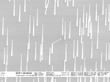
In condensed matter physics, a quantum wire is an electrically conducting wire, in which quantum effects are affecting transport properties. Due to the quantum confinement of conduction electrons in the transverse direction of the wire, their transverse energy is quantized into a series of...
s". Many different types of nanowires exist, including metallic (e.g., Ni
Nickel
Nickel is a chemical element with the chemical symbol Ni and atomic number 28. It is a silvery-white lustrous metal with a slight golden tinge. Nickel belongs to the transition metals and is hard and ductile...
, Pt
Platinum
Platinum is a chemical element with the chemical symbol Pt and an atomic number of 78. Its name is derived from the Spanish term platina del Pinto, which is literally translated into "little silver of the Pinto River." It is a dense, malleable, ductile, precious, gray-white transition metal...
, Au
Gold
Gold is a chemical element with the symbol Au and an atomic number of 79. Gold is a dense, soft, shiny, malleable and ductile metal. Pure gold has a bright yellow color and luster traditionally considered attractive, which it maintains without oxidizing in air or water. Chemically, gold is a...
), semiconducting (e.g., Si
Silicon
Silicon is a chemical element with the symbol Si and atomic number 14. A tetravalent metalloid, it is less reactive than its chemical analog carbon, the nonmetal directly above it in the periodic table, but more reactive than germanium, the metalloid directly below it in the table...
, InP, GaN, etc.), and insulating (e.g., SiO2
Silicon dioxide
The chemical compound silicon dioxide, also known as silica , is an oxide of silicon with the chemical formula '. It has been known for its hardness since antiquity...
, TiO2
Titanium dioxide
Titanium dioxide, also known as titanium oxide or titania, is the naturally occurring oxide of titanium, chemical formula . When used as a pigment, it is called titanium white, Pigment White 6, or CI 77891. Generally it comes in two different forms, rutile and anatase. It has a wide range of...
).
Unanswered Questions