
Silicon on insulator
Encyclopedia
Silicon dioxide
The chemical compound silicon dioxide, also known as silica , is an oxide of silicon with the chemical formula '. It has been known for its hardness since antiquity...
or sapphire
Sapphire
Sapphire is a gemstone variety of the mineral corundum, an aluminium oxide , when it is a color other than red or dark pink; in which case the gem would instead be called a ruby, considered to be a different gemstone. Trace amounts of other elements such as iron, titanium, or chromium can give...
(these types of devices are called silicon on sapphire
Silicon on sapphire
Silicon on sapphire is a hetero-epitaxial process for integrated circuit manufacturing that consists of a thin layer of silicon grown on a sapphire wafer. SOS is part of the Silicon on Insulator family of CMOS technologies...
, or SOS, and are less common). The choice of insulator depends largely on intended application, with sapphire being used for radiation-sensitive applications and silicon dioxide preferred for improved performance and diminished short channel effects in microelectronics devices. The insulating layer and topmost silicon layer also vary widely with application. The first industrial implementation of SOI was announced by IBM in August 1998.
Industry need
Moore's Law
Moore's law describes a long-term trend in the history of computing hardware: the number of transistors that can be placed inexpensively on an integrated circuit doubles approximately every two years....
. Reported benefits of SOI technology relative to conventional silicon (bulk CMOS
CMOS
Complementary metal–oxide–semiconductor is a technology for constructing integrated circuits. CMOS technology is used in microprocessors, microcontrollers, static RAM, and other digital logic circuits...
) processing include:
- Lower parasitic capacitance due to isolation from the bulk silicon, which improves power consumption at matched performance.
- Resistance to latchupLatchupLatchup is a term used in the realm of integrated circuits to describe a particular type of short circuit which can occur in an improperly designed circuit...
due to complete isolation of the n- and p-well structures.
From a manufacturing perspective, SOI substrates are compatible with most conventional fabrication processes. In general, an SOI-based process may be implemented without special equipment or significant retooling of an existing factory. Among challenges unique to SOI are novel metrology requirements to account for the buried oxide layer and concerns about differential stress in the topmost silicon layer.
The primary barrier to SOI implementation is the drastic increase in substrate cost, which contributes an estimated 10–15% increase to total manufacturing costs.
Manufacture of SOI wafers
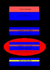
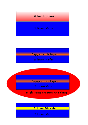
SiO2-based SOI wafers can be produced by several methods:- SIMOX - Separation by IMplantation of OXygen – uses an oxygen ion beam implantationIon implantationIon implantation is a materials engineering process by which ions of a material are accelerated in an electrical field and impacted into another solid. This process is used to change the physical, chemical, or electrical properties of the solid...
process followed by high temperature annealing to create a buried SiO2 layer.
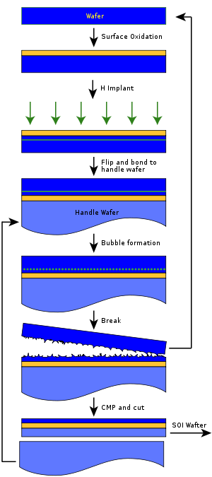
- Wafer bondingWafer bondingWafer bonding is a packaging technology on wafer-level for the fabrication of microelectromechanical systems , nanoelectromechanical systems , microelectronics and optoelectronics, ensuring a mechanically stable and hermetically sealed encapsulation...
– the insulating layer is formed by directly bonding oxidized silicon with a second substrate. The majority of the second substrate is subsequently removed, the remnants forming the topmost Si layer.- One prominent example of a wafer bonding process is the Smart CutSmart CutSmart Cut is a technological process that enables the transfer of very fine layers of crystalline material onto a mechanical support. The application of this technological procedure is used mainly in silicon-on-insulator...
method developed by the French firm SoitecSoitecSoitec is a French semiconductor manufacturer which specializes in the production of Silicon-On-Insulator wafers. Soitec is listed on the Euronext Paris exchange , and its headquarters are located in Bernin,France....
which uses ion implantation followed by controlled exfoliation to determine the thickness of the uppermost silicon layer. - NanoCleave is a technology developed by Silicon Genesis Corporation that separates the silicon via stress at the interface of silicon and silicon-germanium alloy.
- ELTRAN is a technology developed by Canon which is based on porous silicon and water cut.
- One prominent example of a wafer bonding process is the Smart Cut
- Seed methods - wherein the topmost Si layer is grown directly on the insulator. Seed methods require some sort of template for homoepitaxy, which may be achieved by chemical treatment of the insulator, an appropriately oriented crystalline insulator, or vias through the insulator from the underlying substrate.
An exhaustive review of these various manufacturing processes may be found in reference
Use in the microelectronics industry
IBMIBM
International Business Machines Corporation or IBM is an American multinational technology and consulting corporation headquartered in Armonk, New York, United States. IBM manufactures and sells computer hardware and software, and it offers infrastructure, hosting and consulting services in areas...
began to use SOI in the high-end RS64-IV "Istar" PowerPC-AS microprocessor in 2000. Other examples of microprocessors built on SOI technology include AMD's 130 nm, 90 nm, 65 nm and 45 nm single, dual, quad and six core processors since 2001. Freescale adopted SOI in their PowerPC
PowerPC
PowerPC is a RISC architecture created by the 1991 Apple–IBM–Motorola alliance, known as AIM...
7455 CPU in late 2001, currently Freescale is shipping SOI products in 180 nm, 130 nm, 90 nm and 45 nm lines. The 90 nm Power Architecture
Power Architecture
Power Architecture is a broad term to describe similar RISC instruction sets for microprocessors developed and manufactured by such companies as IBM, Freescale, AMCC, Tundra and P.A. Semi...
based processors used in the Xbox 360
Xbox 360
The Xbox 360 is the second video game console produced by Microsoft and the successor to the Xbox. The Xbox 360 competes with Sony's PlayStation 3 and Nintendo's Wii as part of the seventh generation of video game consoles...
, PlayStation 3
PlayStation 3
The is the third home video game console produced by Sony Computer Entertainment and the successor to the PlayStation 2 as part of the PlayStation series. The PlayStation 3 competes with Microsoft's Xbox 360 and Nintendo's Wii as part of the seventh generation of video game consoles...
and Wii
Wii
The Wii is a home video game console released by Nintendo on November 19, 2006. As a seventh-generation console, the Wii primarily competes with Microsoft's Xbox 360 and Sony's PlayStation 3. Nintendo states that its console targets a broader demographic than that of the two others...
use SOI technology as well. Competitive offerings from Intel, however, such as the 65 nm Core 2 and Core 2 Duo microprocessors, are built using conventional bulk CMOS
CMOS
Complementary metal–oxide–semiconductor is a technology for constructing integrated circuits. CMOS technology is used in microprocessors, microcontrollers, static RAM, and other digital logic circuits...
technology. Intel's new 45 nm process will continue to use conventional technology. In January, 2005 Intel researchers reported on an experimental single-chip silicon rib waveguide Raman laser built using SOI.
In November 2010, several news sources indicated that Intel may switch to SOI for the 22 nm
22 nanometer
The 22 nanometer node is the CMOS process step following 32 nm. It was introduced by semiconductor companies in 2011. The typical half-pitch for a memory cell is around 22 nm...
node.. More recently, Intel announced it will NOT go to SOI at 22nm due to costs, and instead will use tri-gate technology.
On the foundry side, July 2006 TSMC
TSMC
Taiwan Semiconductor Manufacturing Company, Limited or TSMC is the world's largest dedicated independent semiconductor foundry, with its headquarters and main operations located in the Hsinchu Science Park in Hsinchu, Taiwan.-Overview:...
claimed no customer wanted SOI, but Chartered Semiconductor devoted a whole fab to SOI.
Use in photonics
SOI wafers are widely used in silicon photonicsSilicon photonics
Silicon photonics is the study and application of photonic systems which use silicon as an optical medium. The silicon is usually patterned with sub-micrometre precision, into microphotonic components. These operate in the infrared, most commonly at the 1.55 micrometre wavelength used by most...
. The crystalline silicon layer on insulator can be used to fabricate optical waveguides and other passive optical devices for integrated optics. The crystalline silicon layer is sandwiched between the buried insulator (Silicon oxide, Sapphire etc.) and top cladding of air (or Silicon oxide or any other low refractive index material). This enables propagation of electromagnetic waves in the waveguides on the basis of total internal reflection.
See also
- Intel TeraHertzIntel TeraHertzIntel TeraHertz was Intel's new design for transistors. It uses new materials such as zirconium dioxide which is a superior insulator reducing current leakages....
- similar technology from Intel. - Wafer (electronics)Wafer (electronics)A wafer is a thin slice of semiconductor material, such as a silicon crystal, used in the fabrication of integrated circuits and other microdevices...
- Wafer bondingWafer bondingWafer bonding is a packaging technology on wafer-level for the fabrication of microelectromechanical systems , nanoelectromechanical systems , microelectronics and optoelectronics, ensuring a mechanically stable and hermetically sealed encapsulation...
External links
- SOI Industry Consortium - a site with extensive information and education for SOI technology
- SOI IP portal - A search engine for SOI IP
- AMDboard - a site with extensive information regarding SOI technology
- Advanced Substrate News - a newsletter about the SOI industry, produced by Soitec.
- MIGAS '04 - The 7th session of MIGAS International Summer School on Advanced Microelectronics, devoted to SOI technology and devices.
- MIGAS '09 - 12th session of the International Summer School on Advanced Microelectronics: "Silicon on Insulator (SOI) Nanodevices"