

Deep Level Transient Spectroscopy
Encyclopedia
Deep Level Transient Spectroscopy (DLTS) is an experimental tool for studying electrically active defects (known as charge carrier
traps) in semiconductor
s. DLTS establishes fundamental defect parameters and measures their concentration in the material. Some of the parameters are considered as defect “finger prints” used for their identifications and analysis.
DLTS investigates defects present in a space charge (depletion
) region of a simple electronic device. The most commonly used are Schottky diode
s or p-n junction
s. In the measurement process the steady-state diode reverse polarization voltage is disturbed by a voltage pulse
. This voltage pulse reduces the electric field in the space charge region and allows free carriers
from the semiconductor bulk to penetrate this region and recharge the defects causing their non-equilibrium charge state. After the pulse, when the voltage returns to its steady-state value, the defects start to emit trapped carriers due to the thermal emission process. The technique observes the device space charge region capacitance
where the defect charge state recovery causes the capacitance transient. The voltage pulse followed by the defect charge state recovery are cycled allowing an application of different signal processing
methods for defect recharging process analysis.
The DLTS technique has a higher sensitivity than almost any other semiconductor diagnostic technique. For example, in silicon
it can detect impurities and defects at a concentration of one part in 1012 of the material host atoms. This feature together with a technical simplicity of its design made it very popular in research labs and semiconductor material production factories.
The DLTS technique was pioneered by D. V. Lang (David Vern Lang of Bell Laboratories) in 1974. US Patent was awarded to Lang in 1975.
or double box-car averaging
technique when the sample temperature is slowly varied (usually in a range from liquid nitrogen
temperature to room temperature 300K
or above). The equipment reference frequency is the voltage pulse repetition rate. In the conventional DLTS method this frequency multiplied by some constant (depending on the hardware used) is called the “rate window”. When during the sample temperature variation the emission rate of carriers from some defect equals to the rate window one obtains in the spectrum a peak. By setting up different rate windows in subsequent DLTS spectra measurements one obtains different temperatures at which some particular peak appears. Having a set of the emission rate and corresponding temperature pairs one can make an Arrhenius plot
which allows for the deduction of defect activation energy
for the thermal emission process. Usually this energy (sometimes called the defect energy level
) together with the plot intersept value are defect parameters used for its identification or analysis.
Recently, DLTS has been used to study quantum dots.
traps are observed by the application of a reverse bias pulse, while minority carrier
traps can be observed when the reverse bias voltage pulses are replaced with light pulses with the photon
energy from the above semiconductor bandgap
spectral range. This method is called Minority Carrier Transient Spectroscopy (MCTS). The minority carrier traps can be also observed for the p-n junction
s by application of forward bias pulses which inject minority carriers into the space charge region. In DLTS plots the minority carrier spectra usually are depicted with an opposite sign of amplitude in respect to the majority carrier trap spectra.
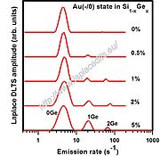
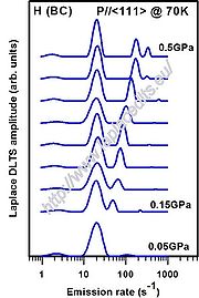 There is an extension to DLTS known as a high resolution Laplace transform DLTS (LDLTS). Laplace DLTS is an isothermal technique in which the capacitance transients are digitized
and averaged at a fixed temperature. Then the defect emission rates are obtained with a use of numerical methods being equivalent to the inverse Laplace transformation. The obtained emission rates are presented as a spectral plot. The main advantage of Laplace DLTS in comparison to conventional DLTS is the substantial increase in energy resolution understood here as an ability to distinguish very similar signals.
Laplace DLTS in combination with uniaxial stress
results in a splitting of the defect energy level. Assuming a random distribution of defects in non-equivalent orientations, the number of split lines and their intensity ratios reflect the symmetry class of the given
defect.
Application of LDLTS to MOS capacitors
needs device polarization voltages in a range where the Fermi level
extrapolated from semiconductor to the semiconductor-oxide interface
intersects this interface within the semiconductor bandgap
range. The electronic interface states present at this interface can trap carriers similarly to defects described above. If their occupancy with electron
s or holes
is disturbed by a small voltage pulse then the device capacitance recovers after the pulse to its initial value as the interface states start to emit carriers. This recovery process can be analyzed with the LDLTS method for different device polarization voltages. Such a procedure allows to obtain the energy state distribution of the interface electronic states at the semiconductor-oxide (or dielectric
) interfaces.
concentration. In cases when this assumption is not fulfilled then the constant capacitance DLTS (CCDLTS) method is used for more accurate determination of the trap concentration. When the defects recharge and their concentration is high then the width of the device space region varies making the analysis of the capacitance transient inaccurate. The additional electronic circuitry maintaining the total device capacitance constant by varying the device bias voltage helps to keep the depletion region width constant. As a result, the varying device voltage reflects the defect recharge process. An analysis of the CCDLTS system using feedback theory was provided by Lau and Lam in 1982.
.) For insulating materials it is difficult or impossible to produce a device having a space region which width could be changed by the external voltage bias and thus the capacitance measurement-based DLTS methods cannot be applied for the defect analysis. Basing on experiences of the thermally stimulated current
(TSC) spectroscopy, the current transients are analyzed with the DLTS methods (I-DLTS), where the light pulses are used for the defect occupancy disturbance. This method in the literature is sometimes called the Photoinduced Transient Spectroscopy (PITS). I-DLTS or PITS are also used for studying defects in the i-region of a p-i-n diode
.
Charge carrier
In physics, a charge carrier is a free particle carrying an electric charge, especially the particles that carry electric currents in electrical conductors. Examples are electrons and ions...
traps) in semiconductor
Semiconductor
A semiconductor is a material with electrical conductivity due to electron flow intermediate in magnitude between that of a conductor and an insulator. This means a conductivity roughly in the range of 103 to 10−8 siemens per centimeter...
s. DLTS establishes fundamental defect parameters and measures their concentration in the material. Some of the parameters are considered as defect “finger prints” used for their identifications and analysis.
DLTS investigates defects present in a space charge (depletion
Depletion region
In semiconductor physics, the depletion region, also called depletion layer, depletion zone, junction region or the space charge region, is an insulating region within a conductive, doped semiconductor material where the mobile charge carriers have diffused away, or have been forced away by an...
) region of a simple electronic device. The most commonly used are Schottky diode
Schottky diode
The Schottky diode is a semiconductor diode with a low forward voltage drop and a very fast switching action...
s or p-n junction
P-n junction
A p–n junction is formed at the boundary between a P-type and N-type semiconductor created in a single crystal of semiconductor by doping, for example by ion implantation, diffusion of dopants, or by epitaxy .If two separate pieces of material were used, this would...
s. In the measurement process the steady-state diode reverse polarization voltage is disturbed by a voltage pulse
Pulse (signal processing)
In signal processing, the term pulse has the following meanings:#A rapid, transient change in the amplitude of a signal from a baseline value to a higher or lower value, followed by a rapid return to the baseline value....
. This voltage pulse reduces the electric field in the space charge region and allows free carriers
Charge carrier
In physics, a charge carrier is a free particle carrying an electric charge, especially the particles that carry electric currents in electrical conductors. Examples are electrons and ions...
from the semiconductor bulk to penetrate this region and recharge the defects causing their non-equilibrium charge state. After the pulse, when the voltage returns to its steady-state value, the defects start to emit trapped carriers due to the thermal emission process. The technique observes the device space charge region capacitance
Capacitance
In electromagnetism and electronics, capacitance is the ability of a capacitor to store energy in an electric field. Capacitance is also a measure of the amount of electric potential energy stored for a given electric potential. A common form of energy storage device is a parallel-plate capacitor...
where the defect charge state recovery causes the capacitance transient. The voltage pulse followed by the defect charge state recovery are cycled allowing an application of different signal processing
Signal processing
Signal processing is an area of systems engineering, electrical engineering and applied mathematics that deals with operations on or analysis of signals, in either discrete or continuous time...
methods for defect recharging process analysis.
The DLTS technique has a higher sensitivity than almost any other semiconductor diagnostic technique. For example, in silicon
Silicon
Silicon is a chemical element with the symbol Si and atomic number 14. A tetravalent metalloid, it is less reactive than its chemical analog carbon, the nonmetal directly above it in the periodic table, but more reactive than germanium, the metalloid directly below it in the table...
it can detect impurities and defects at a concentration of one part in 1012 of the material host atoms. This feature together with a technical simplicity of its design made it very popular in research labs and semiconductor material production factories.
The DLTS technique was pioneered by D. V. Lang (David Vern Lang of Bell Laboratories) in 1974. US Patent was awarded to Lang in 1975.
Conventional DLTS
In conventional DLTS the capacitance transients are investigated by using a lock-in amplifierLock-in amplifier
A lock-in amplifier is a type of amplifier that can extract a signal with a known carrier wave from an extremely noisy environment . It is essentially a homodyne with an extremely low pass filter...
or double box-car averaging
Boxcar function
In mathematics, a boxcar function is any function which is zero over the entirereal line except for a single interval where it is equal to a constant, A; it is a simple step function...
technique when the sample temperature is slowly varied (usually in a range from liquid nitrogen
Liquid nitrogen
Liquid nitrogen is nitrogen in a liquid state at a very low temperature. It is produced industrially by fractional distillation of liquid air. Liquid nitrogen is a colourless clear liquid with density of 0.807 g/mL at its boiling point and a dielectric constant of 1.4...
temperature to room temperature 300K
Kelvin
The kelvin is a unit of measurement for temperature. It is one of the seven base units in the International System of Units and is assigned the unit symbol K. The Kelvin scale is an absolute, thermodynamic temperature scale using as its null point absolute zero, the temperature at which all...
or above). The equipment reference frequency is the voltage pulse repetition rate. In the conventional DLTS method this frequency multiplied by some constant (depending on the hardware used) is called the “rate window”. When during the sample temperature variation the emission rate of carriers from some defect equals to the rate window one obtains in the spectrum a peak. By setting up different rate windows in subsequent DLTS spectra measurements one obtains different temperatures at which some particular peak appears. Having a set of the emission rate and corresponding temperature pairs one can make an Arrhenius plot
Arrhenius equation
The Arrhenius equation is a simple, but remarkably accurate, formula for the temperature dependence of the reaction rate constant, and therefore, rate of a chemical reaction. The equation was first proposed by the Dutch chemist J. H. van 't Hoff in 1884; five years later in 1889, the Swedish...
which allows for the deduction of defect activation energy
Activation energy
In chemistry, activation energy is a term introduced in 1889 by the Swedish scientist Svante Arrhenius that is defined as the energy that must be overcome in order for a chemical reaction to occur. Activation energy may also be defined as the minimum energy required to start a chemical reaction...
for the thermal emission process. Usually this energy (sometimes called the defect energy level
Energy level
A quantum mechanical system or particle that is bound -- that is, confined spatially—can only take on certain discrete values of energy. This contrasts with classical particles, which can have any energy. These discrete values are called energy levels...
) together with the plot intersept value are defect parameters used for its identification or analysis.
Recently, DLTS has been used to study quantum dots.
MCTS and minority-carrier DLTS
For the Schottky diodes, majority carrierCharge carriers in semiconductors
There are two recognized types of charge carriers in semiconductors. One of them is electrons, which carry negative electric charge. In addition, it is convenient to treat the traveling vacancies in the valence-band electron population as the second type of charge carriers, which carry a positive...
traps are observed by the application of a reverse bias pulse, while minority carrier
Charge carriers in semiconductors
There are two recognized types of charge carriers in semiconductors. One of them is electrons, which carry negative electric charge. In addition, it is convenient to treat the traveling vacancies in the valence-band electron population as the second type of charge carriers, which carry a positive...
traps can be observed when the reverse bias voltage pulses are replaced with light pulses with the photon
Photon
In physics, a photon is an elementary particle, the quantum of the electromagnetic interaction and the basic unit of light and all other forms of electromagnetic radiation. It is also the force carrier for the electromagnetic force...
energy from the above semiconductor bandgap
Electronic band structure
In solid-state physics, the electronic band structure of a solid describes those ranges of energy an electron is "forbidden" or "allowed" to have. Band structure derives from the diffraction of the quantum mechanical electron waves in a periodic crystal lattice with a specific crystal system and...
spectral range. This method is called Minority Carrier Transient Spectroscopy (MCTS). The minority carrier traps can be also observed for the p-n junction
P-n junction
A p–n junction is formed at the boundary between a P-type and N-type semiconductor created in a single crystal of semiconductor by doping, for example by ion implantation, diffusion of dopants, or by epitaxy .If two separate pieces of material were used, this would...
s by application of forward bias pulses which inject minority carriers into the space charge region. In DLTS plots the minority carrier spectra usually are depicted with an opposite sign of amplitude in respect to the majority carrier trap spectra.
Laplace DLTS
Digitizing
Digitizing or digitization is the representation of an object, image, sound, document or a signal by a discrete set of its points or samples. The result is called digital representation or, more specifically, a digital image, for the object, and digital form, for the signal...
and averaged at a fixed temperature. Then the defect emission rates are obtained with a use of numerical methods being equivalent to the inverse Laplace transformation. The obtained emission rates are presented as a spectral plot. The main advantage of Laplace DLTS in comparison to conventional DLTS is the substantial increase in energy resolution understood here as an ability to distinguish very similar signals.
Laplace DLTS in combination with uniaxial stress
Stress (physics)
In continuum mechanics, stress is a measure of the internal forces acting within a deformable body. Quantitatively, it is a measure of the average force per unit area of a surface within the body on which internal forces act. These internal forces are a reaction to external forces applied on the body...
results in a splitting of the defect energy level. Assuming a random distribution of defects in non-equivalent orientations, the number of split lines and their intensity ratios reflect the symmetry class of the given
defect.
Application of LDLTS to MOS capacitors
MOSFET
The metal–oxide–semiconductor field-effect transistor is a transistor used for amplifying or switching electronic signals. The basic principle of this kind of transistor was first patented by Julius Edgar Lilienfeld in 1925...
needs device polarization voltages in a range where the Fermi level
Fermi level
The Fermi level is a hypothetical level of potential energy for an electron inside a crystalline solid. Occupying such a level would give an electron a potential energy \epsilon equal to its chemical potential \mu as they both appear in the Fermi-Dirac distribution function,which...
extrapolated from semiconductor to the semiconductor-oxide interface
Interface (chemistry)
An interface is a surface forming a common boundary among two different phases, such as an insoluble solid and a liquid, two immiscible liquids or a liquid and an insoluble gas. The importance of the interface depends on which type of system is being treated: the bigger the quotient area/volume,...
intersects this interface within the semiconductor bandgap
Electronic band structure
In solid-state physics, the electronic band structure of a solid describes those ranges of energy an electron is "forbidden" or "allowed" to have. Band structure derives from the diffraction of the quantum mechanical electron waves in a periodic crystal lattice with a specific crystal system and...
range. The electronic interface states present at this interface can trap carriers similarly to defects described above. If their occupancy with electron
Electron
The electron is a subatomic particle with a negative elementary electric charge. It has no known components or substructure; in other words, it is generally thought to be an elementary particle. An electron has a mass that is approximately 1/1836 that of the proton...
s or holes
Electron hole
An electron hole is the conceptual and mathematical opposite of an electron, useful in the study of physics, chemistry, and electrical engineering. The concept describes the lack of an electron at a position where one could exist in an atom or atomic lattice...
is disturbed by a small voltage pulse then the device capacitance recovers after the pulse to its initial value as the interface states start to emit carriers. This recovery process can be analyzed with the LDLTS method for different device polarization voltages. Such a procedure allows to obtain the energy state distribution of the interface electronic states at the semiconductor-oxide (or dielectric
Dielectric
A dielectric is an electrical insulator that can be polarized by an applied electric field. When a dielectric is placed in an electric field, electric charges do not flow through the material, as in a conductor, but only slightly shift from their average equilibrium positions causing dielectric...
) interfaces.
Constant-Capacitance DLTS
In general, the analysis of the capacitance transients in the DLTS measurements assumes that the concentration of investigated traps is much smaller than the material dopingDoping (semiconductor)
In semiconductor production, doping intentionally introduces impurities into an extremely pure semiconductor for the purpose of modulating its electrical properties. The impurities are dependent upon the type of semiconductor. Lightly and moderately doped semiconductors are referred to as extrinsic...
concentration. In cases when this assumption is not fulfilled then the constant capacitance DLTS (CCDLTS) method is used for more accurate determination of the trap concentration. When the defects recharge and their concentration is high then the width of the device space region varies making the analysis of the capacitance transient inaccurate. The additional electronic circuitry maintaining the total device capacitance constant by varying the device bias voltage helps to keep the depletion region width constant. As a result, the varying device voltage reflects the defect recharge process. An analysis of the CCDLTS system using feedback theory was provided by Lau and Lam in 1982.
I-DLTS and PITS
There is an important shortcoming for DLTS: it cannot be used for insulating materials. (Note: an insulator can be considered as a very large bandgap semiconductorWide bandgap semiconductors
Wide bandgap semiconductors are semiconductor materials with electronic band gaps larger than one or two electronvolts . The exact threshold of "wideness" often depends on the application, such as optoelectronic and power devices...
.) For insulating materials it is difficult or impossible to produce a device having a space region which width could be changed by the external voltage bias and thus the capacitance measurement-based DLTS methods cannot be applied for the defect analysis. Basing on experiences of the thermally stimulated current
Thermally stimulated current
Thermally stimulated current spectroscopy is an experimental technique which is used to study energy levels in semiconductors or insulators . Energy levels are first filled either by optical or electrical injection usually at a relatively low temperature, subsequently electrons or holes are...
(TSC) spectroscopy, the current transients are analyzed with the DLTS methods (I-DLTS), where the light pulses are used for the defect occupancy disturbance. This method in the literature is sometimes called the Photoinduced Transient Spectroscopy (PITS). I-DLTS or PITS are also used for studying defects in the i-region of a p-i-n diode
PIN diode
A PIN diode is a diode with a wide, lightly doped 'near' intrinsic semiconductor region between a p-type semiconductor and an n-type semiconductor region. The p-type and n-type regions are typically heavily doped because they are used for ohmic contacts....
.
See also
- Carrier generation and recombinationCarrier generation and recombinationIn the solid state physics of semiconductors, carrier generation and recombination are processes by which mobile charge carriers are created and eliminated. Carrier generation and recombination processes are fundamental to the operation of many optoelectronic semiconductor devices, such as...
- Bandgap
- Effective massEffective massIn solid state physics, a particle's effective mass is the mass it seems to carry in the semiclassical model of transport in a crystal. It can be shown that electrons and holes in a crystal respond to electric and magnetic fields almost as if they were particles with a mass dependence in their...
- Schottky diodeSchottky diodeThe Schottky diode is a semiconductor diode with a low forward voltage drop and a very fast switching action...
- Frenkel defectFrenkel defectThe Frenkel Defect is shown by ionic solids. The smaller ion is displaced from its lattice position to an interstitial site. It creates a vacancy defect at its original site and an interstitial defect at its new location.-Definition:...
- Schottky defectSchottky defectA Schottky defect is a type of point defect in a crystal lattice named after Walter H. Schottky.The defect forms when oppositely charged ions leave their lattice sites, creating vacancies. These vacancies are formed in stoichiometric units, to maintain an overall neutral charge in the ionic solid....
- Semiconductor deviceSemiconductor deviceSemiconductor devices are electronic components that exploit the electronic properties of semiconductor materials, principally silicon, germanium, and gallium arsenide, as well as organic semiconductors. Semiconductor devices have replaced thermionic devices in most applications...
- Vacancy (chemistry)
- Capacitance voltage profiling
- High-k dielectricHigh-k DielectricThe term high-κ dielectric refers to a material with a high dielectric constant κ used in semiconductor manufacturing processes which replaces the silicon dioxide gate dielectric...