
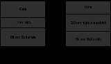
High-k Dielectric
Encyclopedia
The term high-κ dielectric refers to a material with a high dielectric constant
κ (as compared to silicon dioxide
) used in semiconductor manufacturing processes which replaces the silicon dioxide
gate dielectric. The implementation of high-κ gate dielectrics is one of several strategies developed to allow further miniaturization of microelectronic components, colloquially referred to as extending Moore's Law
.
can be modeled as a parallel plate capacitor. Ignoring quantum mechanical and depletion effects from the Si
substrate and gate, the capacitance
C of this parallel plate capacitor
is given by

 Where
Where
Since leakage limitation constrains further reduction of t, an alternative method to increase gate capacitance is alter κ by replacing silicon dioxide with a high-κ material. In such a scenario, a thicker gate layer might be used which can reduce the leakage current
flowing through the structure as well as improving the gate dielectric reliability
.
can be written (using the gradual channel approximation) as
Where
The term VG − Vth is limited in range due to reliability and room temperature operation constraints, since a too large VG would create an undesirable, high electric field across the oxide. Furthermore, Vth cannot easily be reduced below about 200 mV, because leakage currents due to increased oxide leakage (that is, assuming high-κ dielectrics are not available) and subthreshold conduction raise stand-by power consumption to unacceptable levels. (See the industry roadmap , which limits threshold to 200 mV, and Roy et al. ). Thus, according to this simplified list of factors, an increased ID,sat requires a reduction in the channel length or an increase in the gate dielectric capacitance.
the underlying silicon, ensuring a uniform, conformal oxide and high interface quality. As a consequence, development efforts have focused on finding a material with a requisitely high dielectric constant that can be easily integrated into a manufacturing process. Other key considerations include band
alignment to silicon
(which may alter leakage current), film morphology, thermal stability, maintenance of a high mobility
of charge carriers in the channel and minimization of electrical defects in the film/interface. Materials which have received considerable attention are hafnium silicate, zirconium silicate, hafnium dioxide and zirconium dioxide
, typically deposited using atomic layer deposition
.
It is expected that defect states in the high-k dielectric can influence its electrical properties. Defect states can be measured for example by using zero-bias thermally stimulated current, zero-temperature-gradient zero-bias thermally stimulated current spectroscopy
, or inelastic electron tunneling spectroscopy
(IETS).
gate dielectrics since the 1990s, wherein a conventionally formed silicon oxide dielectric is infused with a small amount of nitrogen. The nitride content subtly raises the dielectric constant and is thought to offer other advantages, such as resistance against dopant diffusion through the gate dielectric.
In early 2007, Intel announced the deployment of hafnium
-based high-k dielectrics in conjunction with a metallic gate for components built on 45 nanometer
technologies, and has shipped it in the 2007 processor series codenamed Penryn. At the same time, IBM
announced plans to transition to high-k materials, also hafnium-based, for some products in 2008. While not identified, it is most likely the dielectrics used by these companies are some form of nitrided hafnium silicates (HfSiON). HfO2 and HfSiO are susceptible to crystallization during dopant activation annealing. NEC
Electronics has also announced the use of a HfSiON dielectric in their 55 nm UltimateLowPower technology. However, even HfSiON is susceptible to trap-related leakage currents, which tend to increase with stress over device lifetime. The higher the hafnium concentration, the more severe the issue. However, there is no guarantee that hafnium will be the basis of future high-k dielectrics. The 2006 ITRS
roadmap predicted the implementation of high-k materials to be commonplace in the industry by 2010.
Dielectric constant
The relative permittivity of a material under given conditions reflects the extent to which it concentrates electrostatic lines of flux. In technical terms, it is the ratio of the amount of electrical energy stored in a material by an applied voltage, relative to that stored in a vacuum...
κ (as compared to silicon dioxide
Silicon dioxide
The chemical compound silicon dioxide, also known as silica , is an oxide of silicon with the chemical formula '. It has been known for its hardness since antiquity...
) used in semiconductor manufacturing processes which replaces the silicon dioxide
Silicon dioxide
The chemical compound silicon dioxide, also known as silica , is an oxide of silicon with the chemical formula '. It has been known for its hardness since antiquity...
gate dielectric. The implementation of high-κ gate dielectrics is one of several strategies developed to allow further miniaturization of microelectronic components, colloquially referred to as extending Moore's Law
Moore's Law
Moore's law describes a long-term trend in the history of computing hardware: the number of transistors that can be placed inexpensively on an integrated circuit doubles approximately every two years....
.
Need for high-κ materials
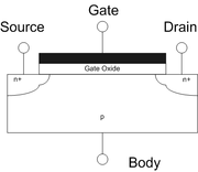
Silicon dioxide has been used as a gate oxide material for decades. As transistors have decreased in size, the thickness of the silicon dioxide gate dielectric has steadily decreased to increase the gate capacitance and thereby drive current and device performance. As the thickness scales below 2 nm, leakage currents due to tunneling increase drastically, leading to unwieldy power consumption and reduced device reliability. Replacing the silicon dioxide gate dielectric with a high-κ material allows increased gate capacitance without the concomitant leakage effects.First principles
The gate oxide in a MOSFETMOSFET
The metal–oxide–semiconductor field-effect transistor is a transistor used for amplifying or switching electronic signals. The basic principle of this kind of transistor was first patented by Julius Edgar Lilienfeld in 1925...
can be modeled as a parallel plate capacitor. Ignoring quantum mechanical and depletion effects from the Si
Silicon
Silicon is a chemical element with the symbol Si and atomic number 14. A tetravalent metalloid, it is less reactive than its chemical analog carbon, the nonmetal directly above it in the periodic table, but more reactive than germanium, the metalloid directly below it in the table...
substrate and gate, the capacitance
Capacitance
In electromagnetism and electronics, capacitance is the ability of a capacitor to store energy in an electric field. Capacitance is also a measure of the amount of electric potential energy stored for a given electric potential. A common form of energy storage device is a parallel-plate capacitor...
C of this parallel plate capacitor
Capacitor
A capacitor is a passive two-terminal electrical component used to store energy in an electric field. The forms of practical capacitors vary widely, but all contain at least two electrical conductors separated by a dielectric ; for example, one common construction consists of metal foils separated...
is given by

- A is the capacitor area
- κ is the relative dielectric constantDielectric constantThe relative permittivity of a material under given conditions reflects the extent to which it concentrates electrostatic lines of flux. In technical terms, it is the ratio of the amount of electrical energy stored in a material by an applied voltage, relative to that stored in a vacuum...
of the material (3.9 for silicon dioxideSilicon dioxideThe chemical compound silicon dioxide, also known as silica , is an oxide of silicon with the chemical formula '. It has been known for its hardness since antiquity...
) - ε0 is the permittivity of free space
- t is the thickness of the capacitor oxide insulator
Since leakage limitation constrains further reduction of t, an alternative method to increase gate capacitance is alter κ by replacing silicon dioxide with a high-κ material. In such a scenario, a thicker gate layer might be used which can reduce the leakage current
Subthreshold leakage
The Subthreshold conduction or the subthreshold leakage or the subthreshold drain current is the current that flows between the source and drain of a MOSFET when the transistor is in subthreshold region, or weak-inversion region, that is, for gate-to-source voltages below the threshold voltage. The...
flowing through the structure as well as improving the gate dielectric reliability
Reliability engineering
Reliability engineering is an engineering field, that deals with the study, evaluation, and life-cycle management of reliability: the ability of a system or component to perform its required functions under stated conditions for a specified period of time. It is often measured as a probability of...
.
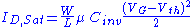
Gate capacitance impact on drive current
The drive current ID for a MOSFETMOSFET
The metal–oxide–semiconductor field-effect transistor is a transistor used for amplifying or switching electronic signals. The basic principle of this kind of transistor was first patented by Julius Edgar Lilienfeld in 1925...
can be written (using the gradual channel approximation) as
Where
- W is the width of the transistor channel
- L is the channel length
- μ is the channel carrier mobility (assumed constant here)
- Cinv is the capacitance density associated with the gate dielectric when the underlying channel is in the inverted state
- VG is the voltage applied to the transistor gate
- VD is the voltage applied to the transistor drain
- Vth is the threshold voltageThreshold voltageThe threshold voltage of a MOSFET is usually defined as the gate voltage where an inversion layer forms at the interface between the insulating layer and the substrate of the transistor. The purpose of the inversion layer's forming is to allow the flow of electrons through the gate-source junction...
The term VG − Vth is limited in range due to reliability and room temperature operation constraints, since a too large VG would create an undesirable, high electric field across the oxide. Furthermore, Vth cannot easily be reduced below about 200 mV, because leakage currents due to increased oxide leakage (that is, assuming high-κ dielectrics are not available) and subthreshold conduction raise stand-by power consumption to unacceptable levels. (See the industry roadmap , which limits threshold to 200 mV, and Roy et al. ). Thus, according to this simplified list of factors, an increased ID,sat requires a reduction in the channel length or an increase in the gate dielectric capacitance.
Materials and considerations
Replacing the silicon dioxide gate dielectric with another material adds complexity to the manufacturing process. Silicon dioxide can be formed by oxidizingThermal oxidation
In microfabrication, thermal oxidation is a way to produce a thin layer of oxide on the surface of a wafer. The technique forces an oxidizing agent to diffuse into the wafer at high temperature and react with it. The rate of oxide growth is often predicted by the Deal-Grove model...
the underlying silicon, ensuring a uniform, conformal oxide and high interface quality. As a consequence, development efforts have focused on finding a material with a requisitely high dielectric constant that can be easily integrated into a manufacturing process. Other key considerations include band
Electronic band structure
In solid-state physics, the electronic band structure of a solid describes those ranges of energy an electron is "forbidden" or "allowed" to have. Band structure derives from the diffraction of the quantum mechanical electron waves in a periodic crystal lattice with a specific crystal system and...
alignment to silicon
Silicon
Silicon is a chemical element with the symbol Si and atomic number 14. A tetravalent metalloid, it is less reactive than its chemical analog carbon, the nonmetal directly above it in the periodic table, but more reactive than germanium, the metalloid directly below it in the table...
(which may alter leakage current), film morphology, thermal stability, maintenance of a high mobility
Electron mobility
In solid-state physics, the electron mobility characterizes how quickly an electron can move through a metal or semiconductor, when pulled by an electric field. In semiconductors, there is an analogous quantity for holes, called hole mobility...
of charge carriers in the channel and minimization of electrical defects in the film/interface. Materials which have received considerable attention are hafnium silicate, zirconium silicate, hafnium dioxide and zirconium dioxide
Zirconium dioxide
Zirconium dioxide , sometimes known as zirconia , is a white crystalline oxide of zirconium. Its most naturally occurring form, with a monoclinic crystalline structure, is the rare mineral baddeleyite. The high temperature cubic crystalline form is rarely found in nature as mineral tazheranite O2...
, typically deposited using atomic layer deposition
Atomic layer deposition
Atomic layer deposition is a thin film deposition technique that is based on the sequential use of a gas phase chemical process. The majority of ALD reactions use two chemicals, typically called precursors. These precursors react with a surface one-at-a-time in a sequential manner...
.
It is expected that defect states in the high-k dielectric can influence its electrical properties. Defect states can be measured for example by using zero-bias thermally stimulated current, zero-temperature-gradient zero-bias thermally stimulated current spectroscopy
Dark current spectroscopy
Dark Current Spectroscopy is a technique that is used to determine contaminants in silicon....
, or inelastic electron tunneling spectroscopy
Inelastic electron tunneling spectroscopy
Inelastic electron tunneling spectroscopy is an experimental tool for studying the vibrations of molecular adsorbates on metal oxides. It yields vibrational spectra of the adsorbates with high resolution Inelastic electron tunneling spectroscopy (IETS) is an experimental tool for studying the...
(IETS).
Use in industry
The industry has employed oxynitrideSilicon oxynitride
Silicon oxynitride is a ceramic material with the chemical formula SiOxNy. While in amorphous forms its composition can continuously vary between SiO2 and Si3N4 , the only known intermediate crystalline phase is Si2N2O...
gate dielectrics since the 1990s, wherein a conventionally formed silicon oxide dielectric is infused with a small amount of nitrogen. The nitride content subtly raises the dielectric constant and is thought to offer other advantages, such as resistance against dopant diffusion through the gate dielectric.
In early 2007, Intel announced the deployment of hafnium
Hafnium
Hafnium is a chemical element with the symbol Hf and atomic number 72. A lustrous, silvery gray, tetravalent transition metal, hafnium chemically resembles zirconium and is found in zirconium minerals. Its existence was predicted by Dmitri Mendeleev in 1869. Hafnium was the penultimate stable...
-based high-k dielectrics in conjunction with a metallic gate for components built on 45 nanometer
45 nanometer
Per the International Technology Roadmap for Semiconductors, the 45 nm technology node should refer to the average half-pitch of a memory cell manufactured at around the 2007–2008 time frame....
technologies, and has shipped it in the 2007 processor series codenamed Penryn. At the same time, IBM
IBM
International Business Machines Corporation or IBM is an American multinational technology and consulting corporation headquartered in Armonk, New York, United States. IBM manufactures and sells computer hardware and software, and it offers infrastructure, hosting and consulting services in areas...
announced plans to transition to high-k materials, also hafnium-based, for some products in 2008. While not identified, it is most likely the dielectrics used by these companies are some form of nitrided hafnium silicates (HfSiON). HfO2 and HfSiO are susceptible to crystallization during dopant activation annealing. NEC
NEC
, a Japanese multinational IT company, has its headquarters in Minato, Tokyo, Japan. NEC, part of the Sumitomo Group, provides information technology and network solutions to business enterprises, communications services providers and government....
Electronics has also announced the use of a HfSiON dielectric in their 55 nm UltimateLowPower technology. However, even HfSiON is susceptible to trap-related leakage currents, which tend to increase with stress over device lifetime. The higher the hafnium concentration, the more severe the issue. However, there is no guarantee that hafnium will be the basis of future high-k dielectrics. The 2006 ITRS
International Technology Roadmap for Semiconductors
The International Technology Roadmap for Semiconductors is a set of documents produced by a group of semiconductor industry experts. These experts are representative of the sponsoring organisations which include the Semiconductor Industry Associations of the US, Europe, Japan, South Korea and...
roadmap predicted the implementation of high-k materials to be commonplace in the industry by 2010.
Further reading
- Review article by Wilk et al. in the Journal of Applied PhysicsJournal of Applied PhysicsThe Journal of Applied Physics is a peer-reviewed scientific journal published since 1931 by the American Institute of Physics. Its emphasis is on the understanding of the physics underpinning modern technology....
- Houssa, M. (Ed.) (2003) High-k Dielectrics Institute of Physics ISBN 0-7503-0906-7 CRC Press Online
- Huff, H.R., Gilmer, D.C. (Ed.) (2005) High Dielectric Constant Materials : VLSI MOSFET applications Springer ISBN 3-540-21081-4
- Demkov, A.A, Navrotsky, A., (Ed.) (2005) Materials Fundamentals of Gate Dielectrics Springer ISBN 1-4020-3077-0
- "High dielectric constant gate oxides for metal oxide Si transistors" Robertson, J. (Rep. Prog. Phys. 69 327-396 2006) Institute Physics Publishing High dielectric constant gate oxides
- Media coverage of March, 2007 Intel/IBM announcements BBC NEWS|Technology|Chips push through nano-barrier, NY Times Article (1/27/07)
- Gusev, E. P. (Ed.) (2006) "Defects in High-k Gate Dielectric Stacks: Nano-Electronic Semiconductor Devices", Springer ISBN 1-402-04366X