
Athlon
Encyclopedia
Athlon is the brand name applied to a series of x86-compatible microprocessor
s designed and manufactured by Advanced Micro Devices
(AMD). The original Athlon (now called Athlon Classic) was the first seventh-generation x86 processor and, in a first, retained the initial performance lead it had over Intel
's competing processors for a significant period of time. The original Athlon also had the distinction of being the first desktop processor to reach speeds of one gigahertz (GHz). AMD has continued using the Athlon name with the Athlon 64
, an eighth-generation processor featuring x86-64
(later renamed AMD64) architecture, and the Athlon II
.
The Athlon made its debut on June 23, 1999. Athlon is the ancient Greek word for "Champion/trophy of the games".
developed strategic partnerships during the late 1990s to improve AMD's presence in the PC market based on the success of the AMD K6
architecture. One major partnership announced in 1998 paired AMD with semiconductor giant Motorola
. In the announcement, Sanders referred to the partnership as creating a "virtual gorilla" that would enable AMD to compete with Intel on fabrication capacity while limiting AMD's financial outlay for new facilities. This partnership also helped to co-develop copper-based semiconductor technology
, which would become a cornerstone of the K7 production process.
In August 1999, AMD released the Athlon (K7) processor. Notably, the design team was led by Dirk Meyer
, who had worked as a lead engineer on multiple Alpha
microprocessors during his employment at DEC
. Jerry Sanders had approached many of the engineering staff to work for AMD as DEC wound down their semiconductor business, and brought in a near-complete team of engineering experts. The balance of the Athlon design team comprised AMD K5
and K6
veterans.
By working with Motorola, AMD was able to refine copper interconnect manufacturing to the production stage about one year before Intel. The revised process permitted 180-nanometer processor production. The accompanying die-shrink resulted in lower power consumption, permitting AMD to increase Athlon clock speeds to the 1 GHz range. Yields on the new process exceeded expectations, permitting AMD to deliver high speed chips in volume in March 2000.
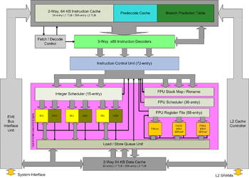 Internally, the Athlon is a fully seventh generation x86 processor, the first of its kind. Like the AMD K5 and K6, the Athlon dynamically buffers internal micro-instructions at runtime resulting from parallel x86 instruction decoding. The CPU is an out-of-order
design, again like previous post-5x86 AMD CPUs. The Athlon utilizes the Alpha 21264
's EV6 bus architecture with double data rate
(DDR) technology. This means that at 100 MHz, the Athlon front side bus actually transfers at a rate similar to a 200 MHz single data rate bus (referred to as 200 MT/s), which was superior to the method used on Intel's Pentium III
(with SDR bus speeds of 100 MHz and 133 MHz).
AMD designed the CPU with more robust x86 instruction decoding capabilities than that of K6, to enhance its ability to keep more data in-flight at once. The Athlon's three decoders could potentially decode three x86 instructions to six microinstructions per clock, although this was somewhat unlikely in real-world use. The critical branch predictor unit, essential to keeping the pipeline busy, was enhanced compared to what was on board the K6. Deeper pipelining with more stages allowed higher clock speeds to be attained. Whereas the AMD K6-III
+ topped out at 570 MHz due to its short pipeline, even when built on the 180 nm process, the Athlon was capable of clocking much higher.
AMD ended its long-time handicap with floating point
x87
performance by designing a super-pipelined, out-of-order, triple-issue floating point unit
. Each of its three units was tailored to be able to calculate an optimal type of instructions with some redundancy. By having separate units, it was possible to operate on more than one floating point instruction at once. This FPU was a huge step forward for AMD. While the K6 FPU had looked anemic compared to the Intel P6
FPU, with Athlon this was no longer the case.
The 3DNow!
floating point
SIMD
technology, again present, received some revisions and a name change to "Enhanced 3DNow!". Additions included DSP
instructions and an implementation of the extended MMX subset of Intel SSE
.
The Athlon's CPU cache
consisted of the typical two levels. Athlon was the first x86 processor with a 128 kB
split level 1 cache; a 2-way associative
, later 16-way, cache separated into 2×64 kB for data and instructions (Harvard architecture
). This cache was double the size of K6's already large 2×32 kB cache, and quadruple the size of Pentium II
and III's 2×16 kB L1 cache. The initial Athlon (Slot A, later called Athlon Classic) used 512 kB of level 2 cache separate from the CPU, on the processor cartridge board, running at 50% to 33% of core speed. This was done because the 250 nm manufacturing process was too large to allow for on-die cache while maintaining cost-effective die size. Later Athlon CPUs, afforded greater transistor budgets by smaller 180 nm
and 130 nm
process nodes, moved to on-die L2 cache at full CPU clock speed.


 The Athlon, later called Athlon Classic, launched on June 23, 1999 and was generally available in August of that year. It demonstrated superior performance compared to the reigning champion, Intel's Pentium III, in every benchmark.
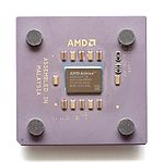
The Athlon Classic is a cartridge-based processor. The design, called Slot A
, was similar to Intel's Slot 1
cartridge used for Pentium II and Pentium III. The mating motherboard
receptacle was the same part used with Intel products but keyed differently to prevent installation of the wrong CPU. The cartridge assembly allowed the use of higher speed cache memory than can be put on the motherboard. Like Pentium II and the Katmai-based Pentium III, the Athlon Classic contained 512 kB of L2 cache. This cache, again like its competitors, ran at a fraction of the core clock rate and had its own 64-bit bus, called a "back-side bus", that allowed concurrent system front side bus and cache accesses. Initially, the L2 cache was run at half the CPU clock speed, on Athlon CPUs clocked up to 700 MHz. Faster Slot-A processors were forced to compromise with cache clock speed and ran at 2/5 (up to 850 MHz) or 1/3 (up to 1 GHz). The SRAM
available at the time was incapable of matching the Athlon's clock scalability, due both to cache chip technology limitations and electrical/cache latency complications of running an external cache at such a high speed.
The Slot-A Athlons were the first multiplier-locked CPUs from AMD. This was partly done to hinder CPU remarking being done by questionable resellers around the globe. AMD's older CPUs could simply be set to run at whatever clock speed the user chose on the motherboard, making it trivial to relabel a CPU and sell it as a faster grade than it was originally intended. These relabeled CPUs were not always stable, being overclocked and not tested properly, and this was damaging to AMD's reputation. Although the Athlon was multiplier locked, crafty enthusiasts eventually discovered that a connector on the PCB of the cartridge could control the multiplier. Eventually a product called the "Goldfingers device" was created that could unlock the CPU, named after the gold connector pads on the processor board that it attached to.
In commercial terms, the Athlon "Classic" was an enormous success—not just because of its own merits, but also because Intel endured a series of major production, design, and quality control issues at this time. In particular, Intel's transition to the 180 nm production process, starting in late 1999 and running through to mid-2000, suffered delays. There was a shortage of Pentium III parts. In contrast, AMD enjoyed a remarkably smooth process transition and had ample supplies available, causing Athlon sales to become quite strong.
The Argon-based Athlon contained 22 million transistors and measured 184 mm2. It was fabricated by AMD in a slightly modified version of their CS44E process, a 0.25 µm complementary metal–oxide–semiconductor (CMOS) process with six levels of aluminium interconnect. "Pluto" and "Orion" Athlons were fabricated in a 0.18 µm process.
Specifications
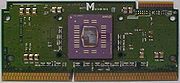 The second generation Athlon, the Thunderbird, debuted on June 5, 2000. This version of the Athlon shipped in a more traditional pin-grid array
(PGA) format that plugged into a socket ("Socket A
") on the motherboard (it also shipped in the slot A package). It was sold at speeds ranging from 600 MHz to 1.4 GHz (Athlon Classics using the Slot A package could clock up to 1 GHz). The major difference, however, was cache design. Just as Intel had done when they replaced the old Katmai-based Pentium III
with the much faster Coppermine-based Pentium III, AMD replaced the 512 kB external reduced-speed cache of the Athlon Classic with 256 kB of on-chip, full-speed exclusive cache. As a general rule, more cache improves performance, but faster cache improves it further still.
AMD changed cache design significantly with the Thunderbird core. With the older Athlon CPUs, the CPU caching was of an inclusive design where data from the L1 is duplicated in the L2 cache. Thunderbird moved to an exclusive design where the L1 cache's contents are not duplicated in the L2. This increases total cache size of the processor and effectively makes caching behave as if there is a very large L1 cache with a slower region (the L2) and a very fast region (the L1). Because of Athlon's very large L1 cache and the exclusive design which turns the L2 cache into basically a "victim cache", the need for high L2 performance and size was lessened. AMD kept the 64-bit L2 cache data bus from the older Athlons, as a result, and allowed it to have a relatively high latency. A simpler L2 cache reduced the possibility of the L2 cache causing clock scaling and yield issues. Still, instead of the 2-way associative scheme used in older Athlons, Thunderbird did move to a more efficient 16-way associative layout.
The Thunderbird was AMD's most successful product since the Am386DX-40
ten years earlier. Mainboard designs had improved considerably by this time, and the initial trickle of Athlon mainboard makers had swollen to include every major manufacturer. AMD's new fab in Dresden
came online, allowing further production increases, and the process technology was improved by a switch to copper interconnects. In October 2000, the Athlon "C" was introduced, raising the mainboard front side bus
speed from 100 MHz to 133 MHz (266 MT/s) and providing roughly 10% extra performance per clock over the "B" model Thunderbird.
Specifications
 AMD released the third-generation Athlon, code-named "Palomino", on October 9, 2001 as the Athlon XP. The "XP" suffix is interpreted to mean eXtreme Performance and also as an unofficial reference to Microsoft Windows XP
. The Athlon XP was marketed using a PR system, which compared its relative performance to an Athlon utilizing the earlier "Thunderbird" core. Athlon XP launched at speeds between 1.33 GHz (PR1500+) and 1.53 GHz (PR1800+), giving AMD the x86 performance lead with the 1800+ model. Less than a month later, it enhanced that lead with the release of the 1600 MHz 1900+, and subsequent 1.67 GHz Athlon XP 2000+ in January, 2002.
Palomino was the first K7 core to include the full SSE
instruction set from the Intel Pentium III
, as well as AMD's 3DNow! Professional
. It is roughly 10% faster than Thunderbird at the same clock speed, thanks in part to the new SIMD functionality and to several additional improvements. The core has enhancements to the K7's TLB
architecture and added a hardware data prefetch
mechanism to take better advantage of available memory bandwidth. Palomino was also the first socketed Athlon officially supporting dual processing, with chips certified for that purpose branded as the Athlon MP.
Changes in core layout also resulted in Palomino being more frugal with its electrical demands, consuming approximately 20% less power than its predecessor, and thus reducing heat output comparatively as well. While the proceeding Athlon "Thunderbird" was capable of clock speeds exceeding 1400 MHz, the power and thermal considerations required to reach those speeds would have made it increasingly impractical as a marketable product. Thus, Palomino's goals of lowered power consumption (and resultant heat produced) allowed AMD to increase performance within a reasonable power envelope. Palomino's design also allowed AMD to continue using the same 180 nm manufacturing process node and core voltages as the proceeding Thunderbird.
Interestingly, the Palomino core actually debuted earlier in the mobile market — creatively branded the Mobile Athlon 4 with the codename "Corvette". It distinctively used a ceramic interposer
much like the Thunderbird instead of the organic pin grid array package used on all later Palomino processors.
Specifications
 The fourth-generation Athlon Thoroughbred was released on 10 June 2002 at 1.8 GHz (Athlon XP PR2200+). The "Thoroughbred" core marked AMD's first production 130 nm silicon, resulting in a significant reduction in die size compared to its 180 nm predecessor.
There came to be two steppings
(revisions) of this core commonly referred to as Tbred-A (cpuid
:6 8 0) and Tbred-B (cpuid
:6 8 1). The initial version (later known as A) was simply a direct die shrink
of the Palomino, and demonstrated that AMD had successfully transitioned to a 130 nm process. While successful in reducing the production cost per processor, the unmodified Palomino design did not demonstrate the expected reduction in heat and clock scalability usually seen when a design is shrunk to a smaller process. As a result, AMD was not able to increase Thoroughbred-A clock speeds much above those of the Palomino it was to replace. Tbred-A was only sold in versions from 1333 MHz to 1800 MHz, and was only able to dis-place the more production-costly Palomino from AMD's lineup.
AMD thus reworked the Thoroughbred's design to better match the process node on which it was produced, in turn creating the Thoroughbred-B. A significant aspect of this redesign was the addition of another ninth "metal layer" to the already quite complex eight-layered Thoroughbred-A. For comparison, the competing Pentium 4 Northwood only utilized six, and its successor Prescott seven layers. While the addition of more layers itself does not improve performance, it gives more flexibility for chip designers routing electrical pathways within a chip, and importantly for the Thoroughbred core, more flexibility in working around electrical bottlenecks that prevented the processor from attaining higher clock speeds. The Tbred-B offered a startling improvement in headroom over the Tbred-A, which made it very popular for overclocking
. The Tbred-A often struggled to reach clock speeds above 1.9Ghz, while the Tbred-B often could easily reach 2.3Ghz and above.
The Thoroughbred line received an increased front side bus clock during its lifetime, from 133 MHz (266 MT/s) to 166 MHz (333 MT/s) improving the processor's ability to access memory and I/O efficiency, and resulted in improved per-clock performance. AMD shifted their PR rating scheme accordingly, making lower clock speeds equate to higher PR ratings.
The Thoroughbred-B was the direct basis for its successor — the Tbred-B with an additional 256 kB of L2 cache (for 512 kB total) became the Barton core.
Specifications
 Fifth-generation Athlon Barton-core processors released in early 2003 with PR ratings of 2500+, 2600+, 2800+, 3000+, and 3200+. While not operating at higher clock rates than Thoroughbred-core processors, they were marked with higher PR-ratings by featuring an increased 512 kB L2 cache; later models additionally supported an increased 200 MHz (400 MT/s) front side bus. The Thorton core was a later variant of the Barton with half of the L2 cache disabled, and thus was functionally identical to the Thoroughbred-B core. The name Thorton is a portmanteau of Thoroughbred and Barton.
By the time of Barton's release, the Northwood-based Pentium 4
had become more than competitive with AMD's processors. Unfortunately for AMD, a simple increase in size of the L2 cache to 512 kB did not have nearly the same impact as it did for Intel's Pentium 4 line, as the Athlon architecture was not nearly as cache-constrained as the Pentium 4. The Athlon's exclusive-cache architecture and shorter pipeline made it less sensitive to L2 cache size, and the Barton only saw an increase of several percent gained in per-clock performance over the Throughbred-B it was derived from. While the increased performance was welcome, it was not sufficient to overtake the Pentium 4 line in overall performance. The PR rating also became somewhat inaccurate because some Barton models with lower clock rates were being given higher PR ratings than higher-clocked Thoroughbred processors. Instances where a computational task did not "benefit more" from the additional cache to make up for the loss in raw clock speed created situations where a lower rated (but faster clocked) Thoroughbred would outperform a higher-rated (but lower clocked) Barton.
The Barton was also used to officially introduce a higher 400 MT/s bus clock for the Socket A platform, which was used to gain some Barton models more efficiency (and increased PR ratings). However, it was clear by this time that Intel's quad-pumped bus was scaling well above AMD's double-pumped EV6 bus. The 800 MT/s bus used by many later Pentium 4 processors was well out of the Athlon XP's reach. In order to reach the same bandwidth levels, the Athlon XP's bus would have to be clocked at levels simply unreachable.
By this point, the four year old Athlon EV6 bus architecture had scaled to its limit. To maintain or exceed the performance of Intel's newer processors would require a significant redesign. The K7 derived Athlons were replaced in March 2003 by the Athlon 64
family, which featured an on-chip memory controller
and a completely new HyperTransport
bus to replace EV6.
Specifications:
Barton (130 nm)
Thorton (130 nm)
 Mobile Athlon XPs (Athlon XP-M) are identical to normal Athlon XPs, apart from running at lower voltages, often lower bus speeds, and not being multiplier
-locked. The lower Vcore rating caused the CPU to have lower power consumption (ideal for battery-powered laptops) and lower heat production. Athlon XP-M CPUs also have a higher-rated heat tolerance, a requirement of the tight conditions within a notebook PC.
The Athlon XP-M replaced the older Mobile Athlon 4. The Mobile Athlon 4 used the older Palomino core, while the Athlon XP-M used the newer Thoroughbred and Barton cores. Some specialized low-power Athlon XP-Ms utilize the microPGA socket 563
rather than the standard Socket A.
The CPUs, like their mobile K6+
predecessors, were also capable of dynamic clock adjustment for power optimization. When the system is idle
, the CPU clocks itself down through a lower bus multiplier and also reduces its voltage. Then, when a program demands more computational resources, the CPU very quickly (there is some latency) returns to intermediate or maximum speed to meet the demand. This technology was marketed as "PowerNow!
". It was similar to Intel's SpeedStep
power saving technique. The feature was controlled by the CPU, motherboard BIOS
, and operating system
. AMD later renamed the technology to Cool'n'Quiet
on their K8-based CPUs (Athlon 64
, etc.), and introduced it for use on desktop PCs as well.
Athlon XP-Ms were popular with desktop overclockers
, as well as underclockers
. The lower voltage requirement and higher heat rating resulted in CPUs that were basically "cherry picked" from the manufacturing line. Being the best of the cores off the line, the CPUs typically were more reliably overclocked than their desktop-headed counterparts. Also, the fact that they were not locked to a single multiplier was a significant simplification for the overclocking process. Some Barton core Athlon XP-Ms have been successfully overclocked to as high as 3.1 GHz.
As stated, the chips were also liked for their underclocking ability. Underclocking is a process of determining the lowest Vcore at which a CPU can remain stable at for a given clock speed. The Athlon XP-M CPUs were capable of running lower voltages per clock rate compared to their desktop siblings. As such, the chips were used in home theater PC
systems due to their high performance and low heat output at low Vcore settings.
Besides not being locked to multiplier, they were also not disabled from SMP operation as were other Athlon XPs. Thus one could use them instead of the more expensive Athlon MP in dual socket A motherboards. Since those boards lacked multiplier and voltage adjustments, and could run only 133 MHz FSB the adjustment could have been made by wire-modding the CPU socket by connecting adjacent CPU pins. It was normal to overclock mobile 2500+ CPU to 2.26 GHz with 17x multiplier, thus being faster than fastest official 2800+ MP CPU running at 2.13 GHz.
Microprocessor
A microprocessor incorporates the functions of a computer's central processing unit on a single integrated circuit, or at most a few integrated circuits. It is a multipurpose, programmable device that accepts digital data as input, processes it according to instructions stored in its memory, and...
s designed and manufactured by Advanced Micro Devices
Advanced Micro Devices
Advanced Micro Devices, Inc. or AMD is an American multinational semiconductor company based in Sunnyvale, California, that develops computer processors and related technologies for commercial and consumer markets...
(AMD). The original Athlon (now called Athlon Classic) was the first seventh-generation x86 processor and, in a first, retained the initial performance lead it had over Intel
Intel Corporation
Intel Corporation is an American multinational semiconductor chip maker corporation headquartered in Santa Clara, California, United States and the world's largest semiconductor chip maker, based on revenue. It is the inventor of the x86 series of microprocessors, the processors found in most...
's competing processors for a significant period of time. The original Athlon also had the distinction of being the first desktop processor to reach speeds of one gigahertz (GHz). AMD has continued using the Athlon name with the Athlon 64
Athlon 64
The Athlon 64 is an eighth-generation, AMD64-architecture microprocessor produced by AMD, released on September 23, 2003. It is the third processor to bear the name Athlon, and the immediate successor to the Athlon XP...
, an eighth-generation processor featuring x86-64
X86-64
x86-64 is an extension of the x86 instruction set. It supports vastly larger virtual and physical address spaces than are possible on x86, thereby allowing programmers to conveniently work with much larger data sets. x86-64 also provides 64-bit general purpose registers and numerous other...
(later renamed AMD64) architecture, and the Athlon II
Athlon II
Athlon II is a family of AMD multi-core 45 nm central processing units, which is aimed at the midrange to budget market and is a complementary product lineup to the Phenom II.-Features:...
.
The Athlon made its debut on June 23, 1999. Athlon is the ancient Greek word for "Champion/trophy of the games".
Background
AMD ex-CEO and founder Jerry SandersJerry Sanders (businessman)
Walter Jeremiah Sanders III was a co-founder and a long-time CEO of the American semiconductor manufacturer Advanced Micro Devices ....
developed strategic partnerships during the late 1990s to improve AMD's presence in the PC market based on the success of the AMD K6
AMD K6
The K6 microprocessor was launched by AMD in 1997. The main advantage of this particular microprocessor is that it was designed to fit into existing desktop designs for Pentium branded CPUs. It was marketed as a product which could perform as well as its Intel Pentium II equivalent but at a...
architecture. One major partnership announced in 1998 paired AMD with semiconductor giant Motorola
Motorola
Motorola, Inc. was an American multinational telecommunications company based in Schaumburg, Illinois, which was eventually divided into two independent public companies, Motorola Mobility and Motorola Solutions on January 4, 2011, after losing $4.3 billion from 2007 to 2009...
. In the announcement, Sanders referred to the partnership as creating a "virtual gorilla" that would enable AMD to compete with Intel on fabrication capacity while limiting AMD's financial outlay for new facilities. This partnership also helped to co-develop copper-based semiconductor technology
Copper-based chips
Copper-based chips are semiconductor integrated circuits, usually microprocessors, which use copper for interconnections. Since copper is a better conductor than aluminium, chips using this technology can have smaller metal components, and use less energy to pass electricity through them...
, which would become a cornerstone of the K7 production process.
In August 1999, AMD released the Athlon (K7) processor. Notably, the design team was led by Dirk Meyer
Dirk Meyer
Derrick R. "Dirk" Meyer was a former Chief Executive Officer of Advanced Micro Devices, serving in the position since July 18, 2008 and resigning on January 10, 2011.- Education :...
, who had worked as a lead engineer on multiple Alpha
DEC Alpha
Alpha, originally known as Alpha AXP, is a 64-bit reduced instruction set computer instruction set architecture developed by Digital Equipment Corporation , designed to replace the 32-bit VAX complex instruction set computer ISA and its implementations. Alpha was implemented in microprocessors...
microprocessors during his employment at DEC
Digital Equipment Corporation
Digital Equipment Corporation was a major American company in the computer industry and a leading vendor of computer systems, software and peripherals from the 1960s to the 1990s...
. Jerry Sanders had approached many of the engineering staff to work for AMD as DEC wound down their semiconductor business, and brought in a near-complete team of engineering experts. The balance of the Athlon design team comprised AMD K5
AMD K5
The K5 was AMD's first x86 processor to be developed entirely in-house. Introduced in March 1996, its primary competition was Intel's Pentium microprocessor. The K5 was an ambitious design, closer to a Pentium Pro than a Pentium regarding technical solutions and internal architecture...
and K6
AMD K6
The K6 microprocessor was launched by AMD in 1997. The main advantage of this particular microprocessor is that it was designed to fit into existing desktop designs for Pentium branded CPUs. It was marketed as a product which could perform as well as its Intel Pentium II equivalent but at a...
veterans.
By working with Motorola, AMD was able to refine copper interconnect manufacturing to the production stage about one year before Intel. The revised process permitted 180-nanometer processor production. The accompanying die-shrink resulted in lower power consumption, permitting AMD to increase Athlon clock speeds to the 1 GHz range. Yields on the new process exceeded expectations, permitting AMD to deliver high speed chips in volume in March 2000.
General architecture
Out-of-order execution
In computer engineering, out-of-order execution is a paradigm used in most high-performance microprocessors to make use of instruction cycles that would otherwise be wasted by a certain type of costly delay...
design, again like previous post-5x86 AMD CPUs. The Athlon utilizes the Alpha 21264
Alpha 21264
The Alpha 21264 was a Digital Equipment Corporation RISC microprocessor introduced in October, 1996. The 21264 implemented the Alpha instruction set architecture .- Description :...
's EV6 bus architecture with double data rate
Double data rate
In computing, a computer bus operating with double data rate transfers data on both the rising and falling edges of the clock signal. This is also known as double pumped, dual-pumped, and double transition....
(DDR) technology. This means that at 100 MHz, the Athlon front side bus actually transfers at a rate similar to a 200 MHz single data rate bus (referred to as 200 MT/s), which was superior to the method used on Intel's Pentium III
Pentium III
The Pentium III brand refers to Intel's 32-bit x86 desktop and mobile microprocessors based on the sixth-generation P6 microarchitecture introduced on February 26, 1999. The brand's initial processors were very similar to the earlier Pentium II-branded microprocessors...
(with SDR bus speeds of 100 MHz and 133 MHz).
AMD designed the CPU with more robust x86 instruction decoding capabilities than that of K6, to enhance its ability to keep more data in-flight at once. The Athlon's three decoders could potentially decode three x86 instructions to six microinstructions per clock, although this was somewhat unlikely in real-world use. The critical branch predictor unit, essential to keeping the pipeline busy, was enhanced compared to what was on board the K6. Deeper pipelining with more stages allowed higher clock speeds to be attained. Whereas the AMD K6-III
AMD K6-III
The K6-III, code-named "Sharptooth", was an x86 microprocessor manufactured by AMD, released on 22 February 1999, with 400 and 450 MHz models. It was the last Socket 7 desktop processor. For an extremely short time after its release, the fastest available desktop processor from Intel was the...
+ topped out at 570 MHz due to its short pipeline, even when built on the 180 nm process, the Athlon was capable of clocking much higher.
AMD ended its long-time handicap with floating point
Floating point
In computing, floating point describes a method of representing real numbers in a way that can support a wide range of values. Numbers are, in general, represented approximately to a fixed number of significant digits and scaled using an exponent. The base for the scaling is normally 2, 10 or 16...
x87
X87
x87 is a floating point-related subset of the x86 architecture instruction set. It originated as an extension of the 8086 instruction set in the form of optional floating point coprocessors that worked in tandem with corresponding x86 CPUs. These microchips had names ending in "87"...
performance by designing a super-pipelined, out-of-order, triple-issue floating point unit
Floating point unit
A floating-point unit is a part of a computer system specially designed to carry out operations on floating point numbers. Typical operations are addition, subtraction, multiplication, division, and square root...
. Each of its three units was tailored to be able to calculate an optimal type of instructions with some redundancy. By having separate units, it was possible to operate on more than one floating point instruction at once. This FPU was a huge step forward for AMD. While the K6 FPU had looked anemic compared to the Intel P6
P6 (microarchitecture)
The P6 microarchitecture is the sixth generation Intel x86 microarchitecture, implemented by the Pentium Pro microprocessor that was introduced in November 1995. It is sometimes referred to as i686. It was succeeded by the NetBurst microarchitecture in 2000, but eventually revived in the Pentium M...
FPU, with Athlon this was no longer the case.
The 3DNow!
3DNow!
3DNow! is an extension to the x86 instruction set developed by Advanced Micro Devices . It adds single instruction multiple data instructions to the base x86 instruction set, enabling it to perform simple vector processing, which improves the performance of many graphic-intensive applications...
floating point
Floating point
In computing, floating point describes a method of representing real numbers in a way that can support a wide range of values. Numbers are, in general, represented approximately to a fixed number of significant digits and scaled using an exponent. The base for the scaling is normally 2, 10 or 16...
SIMD
SIMD
Single instruction, multiple data , is a class of parallel computers in Flynn's taxonomy. It describes computers with multiple processing elements that perform the same operation on multiple data simultaneously...
technology, again present, received some revisions and a name change to "Enhanced 3DNow!". Additions included DSP
Digital signal processing
Digital signal processing is concerned with the representation of discrete time signals by a sequence of numbers or symbols and the processing of these signals. Digital signal processing and analog signal processing are subfields of signal processing...
instructions and an implementation of the extended MMX subset of Intel SSE
Streaming SIMD Extensions
In computing, Streaming SIMD Extensions is a SIMD instruction set extension to the x86 architecture, designed by Intel and introduced in 1999 in their Pentium III series processors as a reply to AMD's 3DNow! . SSE contains 70 new instructions, most of which work on single precision floating point...
.
The Athlon's CPU cache
CPU cache
A CPU cache is a cache used by the central processing unit of a computer to reduce the average time to access memory. The cache is a smaller, faster memory which stores copies of the data from the most frequently used main memory locations...
consisted of the typical two levels. Athlon was the first x86 processor with a 128 kB
Kilobyte
The kilobyte is a multiple of the unit byte for digital information. Although the prefix kilo- means 1000, the term kilobyte and symbol KB have historically been used to refer to either 1024 bytes or 1000 bytes, dependent upon context, in the fields of computer science and information...
split level 1 cache; a 2-way associative
CPU cache
A CPU cache is a cache used by the central processing unit of a computer to reduce the average time to access memory. The cache is a smaller, faster memory which stores copies of the data from the most frequently used main memory locations...
, later 16-way, cache separated into 2×64 kB for data and instructions (Harvard architecture
Harvard architecture
The Harvard architecture is a computer architecture with physically separate storage and signal pathways for instructions and data. The term originated from the Harvard Mark I relay-based computer, which stored instructions on punched tape and data in electro-mechanical counters...
). This cache was double the size of K6's already large 2×32 kB cache, and quadruple the size of Pentium II
Pentium II
The Pentium II brand refers to Intel's sixth-generation microarchitecture and x86-compatible microprocessors introduced on May 7, 1997. Containing 7.5 million transistors, the Pentium II featured an improved version of the first P6-generation core of the Pentium Pro, which contained 5.5 million...
and III's 2×16 kB L1 cache. The initial Athlon (Slot A, later called Athlon Classic) used 512 kB of level 2 cache separate from the CPU, on the processor cartridge board, running at 50% to 33% of core speed. This was done because the 250 nm manufacturing process was too large to allow for on-die cache while maintaining cost-effective die size. Later Athlon CPUs, afforded greater transistor budgets by smaller 180 nm
180 nanometer
The 180 nm process refers to the level of semiconductor process technology that was reached in the 1999–2000 timeframe, by most leading semiconductor companies, like Intel, Texas Instruments, IBM, and TSMC....
and 130 nm
130 nanometer
The 130 nm process refers to the level of semiconductor process technology that was reached in the 2000–2001 timeframe, by most leading semiconductor companies, like Intel, Texas Instruments, IBM, and TSMC....
process nodes, moved to on-die L2 cache at full CPU clock speed.
Athlon "Classic"
The Athlon Classic is a cartridge-based processor. The design, called Slot A
Slot A
Slot A refers to the physical and electrical specification for a 242-lead single-edge-connector used by early versions of AMD's Athlon processor.The Slot A connector allows for a higher bus rate than Socket 7 or Super Socket 7...
, was similar to Intel's Slot 1
Slot 1
Slot 1 refers to the physical and electrical specification for the connector used by some of Intel's microprocessors, including the Pentium Pro, Celeron, Pentium II and the Pentium III...
cartridge used for Pentium II and Pentium III. The mating motherboard
Motherboard
In personal computers, a motherboard is the central printed circuit board in many modern computers and holds many of the crucial components of the system, providing connectors for other peripherals. The motherboard is sometimes alternatively known as the mainboard, system board, or, on Apple...
receptacle was the same part used with Intel products but keyed differently to prevent installation of the wrong CPU. The cartridge assembly allowed the use of higher speed cache memory than can be put on the motherboard. Like Pentium II and the Katmai-based Pentium III, the Athlon Classic contained 512 kB of L2 cache. This cache, again like its competitors, ran at a fraction of the core clock rate and had its own 64-bit bus, called a "back-side bus", that allowed concurrent system front side bus and cache accesses. Initially, the L2 cache was run at half the CPU clock speed, on Athlon CPUs clocked up to 700 MHz. Faster Slot-A processors were forced to compromise with cache clock speed and ran at 2/5 (up to 850 MHz) or 1/3 (up to 1 GHz). The SRAM
Static random access memory
Static random-access memory is a type of semiconductor memory where the word static indicates that, unlike dynamic RAM , it does not need to be periodically refreshed, as SRAM uses bistable latching circuitry to store each bit...
available at the time was incapable of matching the Athlon's clock scalability, due both to cache chip technology limitations and electrical/cache latency complications of running an external cache at such a high speed.
The Slot-A Athlons were the first multiplier-locked CPUs from AMD. This was partly done to hinder CPU remarking being done by questionable resellers around the globe. AMD's older CPUs could simply be set to run at whatever clock speed the user chose on the motherboard, making it trivial to relabel a CPU and sell it as a faster grade than it was originally intended. These relabeled CPUs were not always stable, being overclocked and not tested properly, and this was damaging to AMD's reputation. Although the Athlon was multiplier locked, crafty enthusiasts eventually discovered that a connector on the PCB of the cartridge could control the multiplier. Eventually a product called the "Goldfingers device" was created that could unlock the CPU, named after the gold connector pads on the processor board that it attached to.
In commercial terms, the Athlon "Classic" was an enormous success—not just because of its own merits, but also because Intel endured a series of major production, design, and quality control issues at this time. In particular, Intel's transition to the 180 nm production process, starting in late 1999 and running through to mid-2000, suffered delays. There was a shortage of Pentium III parts. In contrast, AMD enjoyed a remarkably smooth process transition and had ample supplies available, causing Athlon sales to become quite strong.
The Argon-based Athlon contained 22 million transistors and measured 184 mm2. It was fabricated by AMD in a slightly modified version of their CS44E process, a 0.25 µm complementary metal–oxide–semiconductor (CMOS) process with six levels of aluminium interconnect. "Pluto" and "Orion" Athlons were fabricated in a 0.18 µm process.
Specifications
- L1-Cache: 64 + 64 kB (Data + Instructions)
- L2-Cache: 512 kB, external chips on CPU module with 50%, 40% or 33% of CPU speed
- MMX, 3DNow!3DNow!3DNow! is an extension to the x86 instruction set developed by Advanced Micro Devices . It adds single instruction multiple data instructions to the base x86 instruction set, enabling it to perform simple vector processing, which improves the performance of many graphic-intensive applications...
- Slot ASlot ASlot A refers to the physical and electrical specification for a 242-lead single-edge-connector used by early versions of AMD's Athlon processor.The Slot A connector allows for a higher bus rate than Socket 7 or Super Socket 7...
(EV6) - Front side busFront side busA front-side bus is a computer communication interface often used in computers during the 1990s and 2000s.It typically carries data between the central processing unit and a memory controller hub, known as the northbridge....
: 200 MT/s (100 MHz double-pumped) - VCore: 1.6 V (K7), 1.6–1.8 V (K75)
- First release: June 23, 1999 (K7), November 29, 1999 (K75)
- Clockrate: 500–700 MHz (K7), 550–1000 MHz (K75)
Thunderbird (T-Bird)
Pin grid array
A pin grid array, often abbreviated PGA, is a type of integrated circuit packaging. In a PGA, the package is square or roughly square, and the pins are arranged in a regular array on the underside of the package...
(PGA) format that plugged into a socket ("Socket A
Socket A
Socket A is the CPU socket used for AMD processors ranging from the Athlon Thunderbird to the Athlon XP/MP 3200+, and AMD budget processors including the Duron and Sempron. Socket A also supports AMD Geode NX embedded processors...
") on the motherboard (it also shipped in the slot A package). It was sold at speeds ranging from 600 MHz to 1.4 GHz (Athlon Classics using the Slot A package could clock up to 1 GHz). The major difference, however, was cache design. Just as Intel had done when they replaced the old Katmai-based Pentium III
Pentium III
The Pentium III brand refers to Intel's 32-bit x86 desktop and mobile microprocessors based on the sixth-generation P6 microarchitecture introduced on February 26, 1999. The brand's initial processors were very similar to the earlier Pentium II-branded microprocessors...
with the much faster Coppermine-based Pentium III, AMD replaced the 512 kB external reduced-speed cache of the Athlon Classic with 256 kB of on-chip, full-speed exclusive cache. As a general rule, more cache improves performance, but faster cache improves it further still.
AMD changed cache design significantly with the Thunderbird core. With the older Athlon CPUs, the CPU caching was of an inclusive design where data from the L1 is duplicated in the L2 cache. Thunderbird moved to an exclusive design where the L1 cache's contents are not duplicated in the L2. This increases total cache size of the processor and effectively makes caching behave as if there is a very large L1 cache with a slower region (the L2) and a very fast region (the L1). Because of Athlon's very large L1 cache and the exclusive design which turns the L2 cache into basically a "victim cache", the need for high L2 performance and size was lessened. AMD kept the 64-bit L2 cache data bus from the older Athlons, as a result, and allowed it to have a relatively high latency. A simpler L2 cache reduced the possibility of the L2 cache causing clock scaling and yield issues. Still, instead of the 2-way associative scheme used in older Athlons, Thunderbird did move to a more efficient 16-way associative layout.
The Thunderbird was AMD's most successful product since the Am386DX-40
Am386
The Am386 CPU was a 100%-compatible clone of the Intel 80386 design released by AMD in 1991. It sold millions of units, positioning AMD as a legitimate competitor to Intel, rather than being merely a second source for x86 CPUs ....
ten years earlier. Mainboard designs had improved considerably by this time, and the initial trickle of Athlon mainboard makers had swollen to include every major manufacturer. AMD's new fab in Dresden
Dresden
Dresden is the capital city of the Free State of Saxony in Germany. It is situated in a valley on the River Elbe, near the Czech border. The Dresden conurbation is part of the Saxon Triangle metropolitan area....
came online, allowing further production increases, and the process technology was improved by a switch to copper interconnects. In October 2000, the Athlon "C" was introduced, raising the mainboard front side bus
Front side bus
A front-side bus is a computer communication interface often used in computers during the 1990s and 2000s.It typically carries data between the central processing unit and a memory controller hub, known as the northbridge....
speed from 100 MHz to 133 MHz (266 MT/s) and providing roughly 10% extra performance per clock over the "B" model Thunderbird.
Specifications
- L1-Cache: 64 + 64 kB (Data + Instructions)
- L2-Cache: 256 kB, fullspeed
- MMX, 3DNow!3DNow!3DNow! is an extension to the x86 instruction set developed by Advanced Micro Devices . It adds single instruction multiple data instructions to the base x86 instruction set, enabling it to perform simple vector processing, which improves the performance of many graphic-intensive applications...
- Slot ASlot ASlot A refers to the physical and electrical specification for a 242-lead single-edge-connector used by early versions of AMD's Athlon processor.The Slot A connector allows for a higher bus rate than Socket 7 or Super Socket 7...
& Socket ASocket ASocket A is the CPU socket used for AMD processors ranging from the Athlon Thunderbird to the Athlon XP/MP 3200+, and AMD budget processors including the Duron and Sempron. Socket A also supports AMD Geode NX embedded processors...
(EV6) - Front side busFront side busA front-side bus is a computer communication interface often used in computers during the 1990s and 2000s.It typically carries data between the central processing unit and a memory controller hub, known as the northbridge....
: 100 MHz (Slot-A, B-models), 133 MHz (C-models) (200 MT/s, 266 MT/s) - VCore: 1.70–1.75 V
- First release: June 5, 2000
- Clockrate:
- Slot ASlot ASlot A refers to the physical and electrical specification for a 242-lead single-edge-connector used by early versions of AMD's Athlon processor.The Slot A connector allows for a higher bus rate than Socket 7 or Super Socket 7...
: 650–1000 MHz - Socket ASocket ASocket A is the CPU socket used for AMD processors ranging from the Athlon Thunderbird to the Athlon XP/MP 3200+, and AMD budget processors including the Duron and Sempron. Socket A also supports AMD Geode NX embedded processors...
, 100 MHz FSB (B-models): 600–1400 MHz - Socket ASocket ASocket A is the CPU socket used for AMD processors ranging from the Athlon Thunderbird to the Athlon XP/MP 3200+, and AMD budget processors including the Duron and Sempron. Socket A also supports AMD Geode NX embedded processors...
, 133 MHz FSB (C-models): 1000–1400 MHz
- Slot A
Palomino
Windows XP
Windows XP is an operating system produced by Microsoft for use on personal computers, including home and business desktops, laptops and media centers. First released to computer manufacturers on August 24, 2001, it is the second most popular version of Windows, based on installed user base...
. The Athlon XP was marketed using a PR system, which compared its relative performance to an Athlon utilizing the earlier "Thunderbird" core. Athlon XP launched at speeds between 1.33 GHz (PR1500+) and 1.53 GHz (PR1800+), giving AMD the x86 performance lead with the 1800+ model. Less than a month later, it enhanced that lead with the release of the 1600 MHz 1900+, and subsequent 1.67 GHz Athlon XP 2000+ in January, 2002.
Palomino was the first K7 core to include the full SSE
Streaming SIMD Extensions
In computing, Streaming SIMD Extensions is a SIMD instruction set extension to the x86 architecture, designed by Intel and introduced in 1999 in their Pentium III series processors as a reply to AMD's 3DNow! . SSE contains 70 new instructions, most of which work on single precision floating point...
instruction set from the Intel Pentium III
Pentium III
The Pentium III brand refers to Intel's 32-bit x86 desktop and mobile microprocessors based on the sixth-generation P6 microarchitecture introduced on February 26, 1999. The brand's initial processors were very similar to the earlier Pentium II-branded microprocessors...
, as well as AMD's 3DNow! Professional
3DNow!
3DNow! is an extension to the x86 instruction set developed by Advanced Micro Devices . It adds single instruction multiple data instructions to the base x86 instruction set, enabling it to perform simple vector processing, which improves the performance of many graphic-intensive applications...
. It is roughly 10% faster than Thunderbird at the same clock speed, thanks in part to the new SIMD functionality and to several additional improvements. The core has enhancements to the K7's TLB
Translation Lookaside Buffer
A translation lookaside buffer is a CPU cache that memory management hardware uses to improve virtual address translation speed. All current desktop and server processors use a TLB to map virtual and physical address spaces, and it is ubiquitous in any hardware which utilizes virtual memory.The...
architecture and added a hardware data prefetch
Prefetching
Prefetching may refer to:* Instruction prefetch, in computer architecture, a microprocessor speedup technique* Prefetch input queue , in computer architecture, pre-loading machine code from memory...
mechanism to take better advantage of available memory bandwidth. Palomino was also the first socketed Athlon officially supporting dual processing, with chips certified for that purpose branded as the Athlon MP.
Changes in core layout also resulted in Palomino being more frugal with its electrical demands, consuming approximately 20% less power than its predecessor, and thus reducing heat output comparatively as well. While the proceeding Athlon "Thunderbird" was capable of clock speeds exceeding 1400 MHz, the power and thermal considerations required to reach those speeds would have made it increasingly impractical as a marketable product. Thus, Palomino's goals of lowered power consumption (and resultant heat produced) allowed AMD to increase performance within a reasonable power envelope. Palomino's design also allowed AMD to continue using the same 180 nm manufacturing process node and core voltages as the proceeding Thunderbird.
Interestingly, the Palomino core actually debuted earlier in the mobile market — creatively branded the Mobile Athlon 4 with the codename "Corvette". It distinctively used a ceramic interposer
Interposer
An interposer is an electrical interface routing between one socket or connection to another. The purpose of an interposer is to spread a connection to a wider pitch or to reroute a connection to a different connection....
much like the Thunderbird instead of the organic pin grid array package used on all later Palomino processors.
Specifications
- L1-Cache: 64 + 64 kB (Data + Instructions)
- L2-Cache: 256 kB, fullspeed
- MMX, 3DNow!3DNow!3DNow! is an extension to the x86 instruction set developed by Advanced Micro Devices . It adds single instruction multiple data instructions to the base x86 instruction set, enabling it to perform simple vector processing, which improves the performance of many graphic-intensive applications...
, SSEStreaming SIMD ExtensionsIn computing, Streaming SIMD Extensions is a SIMD instruction set extension to the x86 architecture, designed by Intel and introduced in 1999 in their Pentium III series processors as a reply to AMD's 3DNow! . SSE contains 70 new instructions, most of which work on single precision floating point... - Socket ASocket ASocket A is the CPU socket used for AMD processors ranging from the Athlon Thunderbird to the Athlon XP/MP 3200+, and AMD budget processors including the Duron and Sempron. Socket A also supports AMD Geode NX embedded processors...
(EV6) - Front side busFront side busA front-side bus is a computer communication interface often used in computers during the 1990s and 2000s.It typically carries data between the central processing unit and a memory controller hub, known as the northbridge....
: 133 MHz (266 MT/s) - VCore: 1.50 to 1.75 V
- Power consumption: 68 W
- First release: October 9, 2001
- Clockrate:
- Athlon 4: 850–1400 MHz
- Athlon XP: 1333–1733 MHz (1500+ to 2100+)
- Athlon MP: 1000–1733 MHz
Thoroughbred (T-Bred)
There came to be two steppings
Stepping level
The term stepping level in the context of CPU architecture or integrated circuitry is a version number.Stepping level refers to the introduction or revision of the lithographic mask or masks within the set of plates that generate the pattern that produces the CPU or integrated circuit...
(revisions) of this core commonly referred to as Tbred-A (cpuid
CPUID
The CPUID opcode is a processor supplementary instruction for the x86 architecture. It was introduced by Intel in 1993 when it introduced the Pentium and SL-Enhanced 486 processors....
:6 8 0) and Tbred-B (cpuid
CPUID
The CPUID opcode is a processor supplementary instruction for the x86 architecture. It was introduced by Intel in 1993 when it introduced the Pentium and SL-Enhanced 486 processors....
:6 8 1). The initial version (later known as A) was simply a direct die shrink
Die shrink
The term "die shrink" refers to a simple semiconductor scaling of semiconductor devices, mainly transistors. The act of shrinking a die is to create a somewhat identical circuitry using a more advanced fabrication process, usually involving an advance of lithographic node...
of the Palomino, and demonstrated that AMD had successfully transitioned to a 130 nm process. While successful in reducing the production cost per processor, the unmodified Palomino design did not demonstrate the expected reduction in heat and clock scalability usually seen when a design is shrunk to a smaller process. As a result, AMD was not able to increase Thoroughbred-A clock speeds much above those of the Palomino it was to replace. Tbred-A was only sold in versions from 1333 MHz to 1800 MHz, and was only able to dis-place the more production-costly Palomino from AMD's lineup.
AMD thus reworked the Thoroughbred's design to better match the process node on which it was produced, in turn creating the Thoroughbred-B. A significant aspect of this redesign was the addition of another ninth "metal layer" to the already quite complex eight-layered Thoroughbred-A. For comparison, the competing Pentium 4 Northwood only utilized six, and its successor Prescott seven layers. While the addition of more layers itself does not improve performance, it gives more flexibility for chip designers routing electrical pathways within a chip, and importantly for the Thoroughbred core, more flexibility in working around electrical bottlenecks that prevented the processor from attaining higher clock speeds. The Tbred-B offered a startling improvement in headroom over the Tbred-A, which made it very popular for overclocking
Overclocking
Overclocking is the process of operating a computer component at a higher clock rate than it was designed for or was specified by the manufacturer, but some manufacturers purposely underclock their components to improve battery life. Many people just overclock or 'rightclock' their hardware to...
. The Tbred-A often struggled to reach clock speeds above 1.9Ghz, while the Tbred-B often could easily reach 2.3Ghz and above.
The Thoroughbred line received an increased front side bus clock during its lifetime, from 133 MHz (266 MT/s) to 166 MHz (333 MT/s) improving the processor's ability to access memory and I/O efficiency, and resulted in improved per-clock performance. AMD shifted their PR rating scheme accordingly, making lower clock speeds equate to higher PR ratings.
The Thoroughbred-B was the direct basis for its successor — the Tbred-B with an additional 256 kB of L2 cache (for 512 kB total) became the Barton core.
Specifications
- L1-Cache: 64 + 64 kB (Data + Instructions)
- L2-Cache: 256 kB, fullspeed
- MMX, 3DNow!3DNow!3DNow! is an extension to the x86 instruction set developed by Advanced Micro Devices . It adds single instruction multiple data instructions to the base x86 instruction set, enabling it to perform simple vector processing, which improves the performance of many graphic-intensive applications...
, SSEStreaming SIMD ExtensionsIn computing, Streaming SIMD Extensions is a SIMD instruction set extension to the x86 architecture, designed by Intel and introduced in 1999 in their Pentium III series processors as a reply to AMD's 3DNow! . SSE contains 70 new instructions, most of which work on single precision floating point... - Socket ASocket ASocket A is the CPU socket used for AMD processors ranging from the Athlon Thunderbird to the Athlon XP/MP 3200+, and AMD budget processors including the Duron and Sempron. Socket A also supports AMD Geode NX embedded processors...
(EV6) - Front side busFront side busA front-side bus is a computer communication interface often used in computers during the 1990s and 2000s.It typically carries data between the central processing unit and a memory controller hub, known as the northbridge....
: 133/166 MHz (266/333 MT/s) - VCore: 1.50–1.65 V
- First release: June 10, 2002 (A), August 21, 2002 (B)
- Clockrate:
- Thoroughbred "A": 1400–1800 MHz (1600+ to 2200+)
- Thoroughbred "B": 1400–2250 MHz (1600+ to 2800+)
- 133 MHz FSB: 1400–2133 MHz (1600+ to 2600+)
- 166 MHz FSB: 2083–2250 MHz (2600+ to 2800+)
Barton and Thorton
By the time of Barton's release, the Northwood-based Pentium 4
Pentium 4
Pentium 4 was a line of single-core desktop and laptop central processing units , introduced by Intel on November 20, 2000 and shipped through August 8, 2008. They had a 7th-generation x86 microarchitecture, called NetBurst, which was the company's first all-new design since the introduction of the...
had become more than competitive with AMD's processors. Unfortunately for AMD, a simple increase in size of the L2 cache to 512 kB did not have nearly the same impact as it did for Intel's Pentium 4 line, as the Athlon architecture was not nearly as cache-constrained as the Pentium 4. The Athlon's exclusive-cache architecture and shorter pipeline made it less sensitive to L2 cache size, and the Barton only saw an increase of several percent gained in per-clock performance over the Throughbred-B it was derived from. While the increased performance was welcome, it was not sufficient to overtake the Pentium 4 line in overall performance. The PR rating also became somewhat inaccurate because some Barton models with lower clock rates were being given higher PR ratings than higher-clocked Thoroughbred processors. Instances where a computational task did not "benefit more" from the additional cache to make up for the loss in raw clock speed created situations where a lower rated (but faster clocked) Thoroughbred would outperform a higher-rated (but lower clocked) Barton.
The Barton was also used to officially introduce a higher 400 MT/s bus clock for the Socket A platform, which was used to gain some Barton models more efficiency (and increased PR ratings). However, it was clear by this time that Intel's quad-pumped bus was scaling well above AMD's double-pumped EV6 bus. The 800 MT/s bus used by many later Pentium 4 processors was well out of the Athlon XP's reach. In order to reach the same bandwidth levels, the Athlon XP's bus would have to be clocked at levels simply unreachable.
By this point, the four year old Athlon EV6 bus architecture had scaled to its limit. To maintain or exceed the performance of Intel's newer processors would require a significant redesign. The K7 derived Athlons were replaced in March 2003 by the Athlon 64
AMD K8
The AMD K8 is a computer processor microarchitecture designed by AMD as the successor to the AMD K7 microarchitecture. The K8 was the first implementation of the AMD64 64-bit extension to the x86 processor architecture.Processors based on the K8 core include:...
family, which featured an on-chip memory controller
Memory controller
The memory controller is a digital circuit which manages the flow of data going to and from the main memory. It can be a separate chip or integrated into another chip, such as on the die of a microprocessor...
and a completely new HyperTransport
HyperTransport
HyperTransport , formerly known as Lightning Data Transport , is a technology for interconnection of computer processors. It is a bidirectional serial/parallel high-bandwidth, low-latency point-to-point link that was introduced on April 2, 2001...
bus to replace EV6.
Specifications:
Barton (130 nm)
- L1-Cache: 64 + 64 kB (Data + Instructions)
- L2-Cache: 512 kB, fullspeed
- MMX, 3DNow!3DNow!3DNow! is an extension to the x86 instruction set developed by Advanced Micro Devices . It adds single instruction multiple data instructions to the base x86 instruction set, enabling it to perform simple vector processing, which improves the performance of many graphic-intensive applications...
, SSEStreaming SIMD ExtensionsIn computing, Streaming SIMD Extensions is a SIMD instruction set extension to the x86 architecture, designed by Intel and introduced in 1999 in their Pentium III series processors as a reply to AMD's 3DNow! . SSE contains 70 new instructions, most of which work on single precision floating point... - Socket ASocket ASocket A is the CPU socket used for AMD processors ranging from the Athlon Thunderbird to the Athlon XP/MP 3200+, and AMD budget processors including the Duron and Sempron. Socket A also supports AMD Geode NX embedded processors...
(EV6) - Front side busFront side busA front-side bus is a computer communication interface often used in computers during the 1990s and 2000s.It typically carries data between the central processing unit and a memory controller hub, known as the northbridge....
: 166/200 MHz (333/400 MT/s) - VCore: 1.65 V
- First release: February 10, 2003
- Clockrate: 1833–2333 MHz (2500+ to 3200+)
- 166 MHz FSB: 1833–2333 MHz (2500+ to 3200+)
- 200 MHz FSB: 2100, 2200 MHz (3000+, 3200+)
Thorton (130 nm)
- L1-Cache: 64 + 64 kB (Data + Instructions)
- L2-Cache: 256 kB, fullspeed
- MMX, 3DNow!3DNow!3DNow! is an extension to the x86 instruction set developed by Advanced Micro Devices . It adds single instruction multiple data instructions to the base x86 instruction set, enabling it to perform simple vector processing, which improves the performance of many graphic-intensive applications...
, SSEStreaming SIMD ExtensionsIn computing, Streaming SIMD Extensions is a SIMD instruction set extension to the x86 architecture, designed by Intel and introduced in 1999 in their Pentium III series processors as a reply to AMD's 3DNow! . SSE contains 70 new instructions, most of which work on single precision floating point... - Socket ASocket ASocket A is the CPU socket used for AMD processors ranging from the Athlon Thunderbird to the Athlon XP/MP 3200+, and AMD budget processors including the Duron and Sempron. Socket A also supports AMD Geode NX embedded processors...
(EV6) - Front side busFront side busA front-side bus is a computer communication interface often used in computers during the 1990s and 2000s.It typically carries data between the central processing unit and a memory controller hub, known as the northbridge....
: 133/166/200 MHz (266/333/400 MT/s) - VCore: 1.50–1.65 V
- First release: September 2003
- Clockrate: 1667–2200 MHz (2000+ to 3100+)
- 133 MHz FSB: 1600–2133 MHz (2000+ to 2600+)
- 166 MHz FSB: 2083 MHz (2600+)
- 200 MHz FSB: 2200 MHz (3100+)
Mobile Athlon XP
CPU multiplier
In computing, the clock multiplier measures the ratio of an internal CPU clock rate to the externally supplied clock. A CPU with a 10x multiplier will thus see 10 internal cycles for every external clock cycle...
-locked. The lower Vcore rating caused the CPU to have lower power consumption (ideal for battery-powered laptops) and lower heat production. Athlon XP-M CPUs also have a higher-rated heat tolerance, a requirement of the tight conditions within a notebook PC.
The Athlon XP-M replaced the older Mobile Athlon 4. The Mobile Athlon 4 used the older Palomino core, while the Athlon XP-M used the newer Thoroughbred and Barton cores. Some specialized low-power Athlon XP-Ms utilize the microPGA socket 563
Socket 563
Socket 563 is a microPGA CPU socket used exclusively for low-power Athlon XP-M processors .This socket can usually be found in laptops and requires a low-power mobile part in a special 563-pin µPGA package which is different from the Socket A package used for other Athlon processors.There are...
rather than the standard Socket A.
The CPUs, like their mobile K6+
AMD K6-III
The K6-III, code-named "Sharptooth", was an x86 microprocessor manufactured by AMD, released on 22 February 1999, with 400 and 450 MHz models. It was the last Socket 7 desktop processor. For an extremely short time after its release, the fastest available desktop processor from Intel was the...
predecessors, were also capable of dynamic clock adjustment for power optimization. When the system is idle
Idle
Idle is a term which generally refers to a lack of motion and/or energy.- Uses :In describing a person or machine, idle means the act of nothing or no work...
, the CPU clocks itself down through a lower bus multiplier and also reduces its voltage. Then, when a program demands more computational resources, the CPU very quickly (there is some latency) returns to intermediate or maximum speed to meet the demand. This technology was marketed as "PowerNow!
PowerNow!
PowerNow! is speed throttling and power saving technology of AMD's processors used in laptops. The CPU's clock speed and VCore are automatically decreased when the computer is under low load or idle, to save battery power, reduce heat and noise...
". It was similar to Intel's SpeedStep
SpeedStep
SpeedStep is a trademark for a series of dynamic frequency scaling technologies built into some Intel microprocessors that allow the clock speed of the processor to be dynamically changed by software...
power saving technique. The feature was controlled by the CPU, motherboard BIOS
BIOS
In IBM PC compatible computers, the basic input/output system , also known as the System BIOS or ROM BIOS , is a de facto standard defining a firmware interface....
, and operating system
Operating system
An operating system is a set of programs that manage computer hardware resources and provide common services for application software. The operating system is the most important type of system software in a computer system...
. AMD later renamed the technology to Cool'n'Quiet
Cool'n'Quiet
Cool'n'Quiet is a CPU speed throttling and power saving technology introduced by AMD with its Athlon 64 processor line. It works by reducing the processor's clock rate and voltage when the processor is idle. The aim of this technology is to reduce overall power consumption and lower heat...
on their K8-based CPUs (Athlon 64
Athlon 64
The Athlon 64 is an eighth-generation, AMD64-architecture microprocessor produced by AMD, released on September 23, 2003. It is the third processor to bear the name Athlon, and the immediate successor to the Athlon XP...
, etc.), and introduced it for use on desktop PCs as well.
Athlon XP-Ms were popular with desktop overclockers
Overclocking
Overclocking is the process of operating a computer component at a higher clock rate than it was designed for or was specified by the manufacturer, but some manufacturers purposely underclock their components to improve battery life. Many people just overclock or 'rightclock' their hardware to...
, as well as underclockers
Underclocking
Underclocking, also known as downclocking, is the practice of modifying a synchronous circuit's timing settings to run at a lower clock rate than it was specified to operate at. It may be said to be the computer equivalent of driving a car below the speed limit...
. The lower voltage requirement and higher heat rating resulted in CPUs that were basically "cherry picked" from the manufacturing line. Being the best of the cores off the line, the CPUs typically were more reliably overclocked than their desktop-headed counterparts. Also, the fact that they were not locked to a single multiplier was a significant simplification for the overclocking process. Some Barton core Athlon XP-Ms have been successfully overclocked to as high as 3.1 GHz.
As stated, the chips were also liked for their underclocking ability. Underclocking is a process of determining the lowest Vcore at which a CPU can remain stable at for a given clock speed. The Athlon XP-M CPUs were capable of running lower voltages per clock rate compared to their desktop siblings. As such, the chips were used in home theater PC
Home theater PC
A Home Theater PC or Media Center appliance is a convergence device that combines some or all the capabilities of a personal computer with a software application that supports video, photo, music playback, and sometimes video recording functionality...
systems due to their high performance and low heat output at low Vcore settings.
Besides not being locked to multiplier, they were also not disabled from SMP operation as were other Athlon XPs. Thus one could use them instead of the more expensive Athlon MP in dual socket A motherboards. Since those boards lacked multiplier and voltage adjustments, and could run only 133 MHz FSB the adjustment could have been made by wire-modding the CPU socket by connecting adjacent CPU pins. It was normal to overclock mobile 2500+ CPU to 2.26 GHz with 17x multiplier, thus being faster than fastest official 2800+ MP CPU running at 2.13 GHz.
Athlon competitors
- Intel Pentium IIIPentium IIIThe Pentium III brand refers to Intel's 32-bit x86 desktop and mobile microprocessors based on the sixth-generation P6 microarchitecture introduced on February 26, 1999. The brand's initial processors were very similar to the earlier Pentium II-branded microprocessors...
, Pentium 4Pentium 4Pentium 4 was a line of single-core desktop and laptop central processing units , introduced by Intel on November 20, 2000 and shipped through August 8, 2008. They had a 7th-generation x86 microarchitecture, called NetBurst, which was the company's first all-new design since the introduction of the...
, and CeleronCeleronCeleron is a brand name given by Intel Corp. to a number of different x86 computer microprocessor models targeted at budget personal computers.... - VIA C3VIA C3The VIA C3 is a family of x86 central processing units for personal computers designed by Centaur Technology and sold by VIA Technologies. The different CPU cores are built following the design methodology of Centaur Technology.-Samuel 2 and Ezra cores:...
and C7VIA C7The VIA C7 is an x86 central processing unit designed by Centaur Technology and sold by VIA Technologies.- Product history :The C7 delivers a number of improvements to the older VIA C3 cores but is nearly identical to the latest VIA C3 Nehemiah core. The C7 was officially launched in May 2005,... - Transmeta EfficeonEfficeonThe Efficeon processor is Transmeta's second-generation 256-bit VLIW design which employs a software engine to convert code written for x86 processors to the native instruction set of the chip...
Supercomputers
The fastest supercomputers based on AthlonMP:- Rutgers University, Department of Physics & Astronomy. Machine: NOW Cluster — AMD Athlon. CPU: 512 AthlonMP (1.65 GHz). Rmax: 794 GFLOPS.
See also
- List of AMD Athlon microprocessors
- List of AMD Duron microprocessors
- List of AMD Athlon XP microprocessors
- List of AMD Athlon 64 microprocessors
- List of AMD Sempron microprocessors
External links
- cpu-collection.de AMD Athlon processor images and descriptions
- amdboard.com AMD Athlon/Duron/Sempron CPU identification and OPN breakdown
- AMD's Technical Specifications for 7th generation CPUs (.pdf)
- Easy identification with Interactive AMD product ID
- Xbit Labs EV6 vs GTL+ System Bus
- motherboards.org Unlocking the Duron and Athlon Using the Pencil Trick