
Electron Beam Physical Vapor Deposition
Encyclopedia
Electron Beam Physical Vapor Deposition or EBPVD is a form of physical vapor deposition
in which a target anode is bombarded with an electron beam given off by a charged tungsten filament under high vacuum. The electron beam causes atoms from the target to transform into the gaseous phase. These atoms then precipitate into solid form, coating everything in the vacuum chamber (within line of sight) with a thin layer of the anode material.
industry to grow electronic materials, in the aerospace
industry to form thermal and chemical barrier coatings to protect surfaces against corrosive environments, in optics to impart the desired reflective and transmissive properties to a substrate and elswhere in industry to modify surfaces to have a variety of desired properties. The deposition process can be broadly classified into physical vapor deposition
(PVD) and chemical vapor deposition
(CVD). In CVD, the film growth takes place at high temperatures, leading to the formation of corrosive gaseous products, and it may leave impurities in the film. The PVD process can be carried out at lower deposition temperatures and without corrosive products, but deposition rates are typically lower. Electron
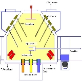
beam physical vapor deposition, however, yields a high deposition rate from 0.1 μm / min to 100 μm / min at relatively low substrate temperatures, with very high material utilization efficiency. The schematic of an EBPVD system is shown in Fig 1.
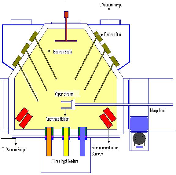
of 10-4 Torr
. The material to be evaporated is in the form of ingots. There are as many as six electron guns, each having a power from tens to hundreds of kW. Electron beams can be generated by thermionic emission
, field electron emission or the anodic arc method. The generated electron beam is accelerated to a high kinetic energy and focused towards the ingot. When the accelerating voltage is between 20 kV – 25 kV and the beam current is a few amperes, 85% of the kinetic energy of the electrons is converted into thermal energy as the beam bombards the surface of the ingot. The surface temperature of the ingot increases resulting in the formation of a liquid melt. Although some of incident electron energy is lost in the excitation of X-rays and secondary emission, the liquid ingot material evaporates under vacuum.
The ingot itself is enclosed in a copper
crucible, which is cooled by water
circulation. The level of molten liquid pool on the surface of the ingot is kept constant by vertical displacement of the ingot. The number of ingot feeders depends upon the material to be deposited. The evaporation rate may be of the order of 10-2 g/cm2 sec.
carbides like titanium carbide
and borides like titanium boride
and zirconium boride can evaporate without undergoing decomposition in the vapor phase. These compounds are deposited by direct evaporation. In this process these compounds, compacted in the form of an ingot, are evaporated in vacuum by the focused high energy electron beam and the vapors are directly condensed over the substrate.
Certain refractory oxides and carbides undergo fragmentation during their evaporation by the electron
beam, resulting in a stoichiometry that is different from the initial material. For example, alumina, when evaporated by electron beam, dissociates into aluminum, AlO3 and Al2O. Some refractory carbides like silicon carbide and tungsten carbide decompose upon heating and the dissociated elements have different volatilities. These compounds can be deposited on the substrate either by reactive evaporation or by co-evaporation. In the reactive evaporation process, the metal
is evaporated from the ingot by the electron beam. The vapors are carried by the reactive gas, which is oxygen in case of metal oxides or acetylene
in case of metal carbides. When the thermodynamic conditions are met, the vapors react with the gas in the vicinity of the substrate to form films. Metal carbide films can also be deposited by co-evaporation
. In this process, two ingots are used, one for metal and the other for carbon
. Each ingot is heated with a different beam energy so that their evaporation rate can be controlled. As the vapors arrive at the surface, they chemically combine under proper thermodynamic conditions to form a metal carbide film.
of 200 V – 400 V can be applied to the substrate. Often, focused high energy electrons from one of the electron guns or infrared light from heater lamps is used to preheat the substrate.
sources are used for substrate etching
and cleaning, sputtering
the target and controlling the microstructure
of the substrate. The ion beams bombard the surface and alter the microstructure of the film. When the deposition reaction takes place on the hot substrate surface, the films can develop an internal tensile stress due to the mismatch in the coefficient of thermal expansion between the substrate and the film. High energy ions can be used to bombard these ceramic thermal barrier coatings and change the tensile stress into compressive stress. Ion bombardment also increases the density of the film, changes the grain size and modifies amorphous films to polycrystalline
films. Low energy
ions are used for the surfaces of semiconductor films.
resistant and thermal barrier coatings in aerospace industries, hard coatings for cutting
and tool
industries, and electronic and optical films for semiconductor industries.
Physical vapor deposition
Physical vapor deposition is a variety of vacuum deposition and is a general term used to describe any of a variety of methods to deposit thin films by the condensation of a vaporized form of the desired film material onto various workpiece surfaces...
in which a target anode is bombarded with an electron beam given off by a charged tungsten filament under high vacuum. The electron beam causes atoms from the target to transform into the gaseous phase. These atoms then precipitate into solid form, coating everything in the vacuum chamber (within line of sight) with a thin layer of the anode material.
Introduction
Thin film deposition is a process applied in the semiconductorSemiconductor
A semiconductor is a material with electrical conductivity due to electron flow intermediate in magnitude between that of a conductor and an insulator. This means a conductivity roughly in the range of 103 to 10−8 siemens per centimeter...
industry to grow electronic materials, in the aerospace
Aerospace
Aerospace comprises the atmosphere of Earth and surrounding space. Typically the term is used to refer to the industry that researches, designs, manufactures, operates, and maintains vehicles moving through air and space...
industry to form thermal and chemical barrier coatings to protect surfaces against corrosive environments, in optics to impart the desired reflective and transmissive properties to a substrate and elswhere in industry to modify surfaces to have a variety of desired properties. The deposition process can be broadly classified into physical vapor deposition
Physical vapor deposition
Physical vapor deposition is a variety of vacuum deposition and is a general term used to describe any of a variety of methods to deposit thin films by the condensation of a vaporized form of the desired film material onto various workpiece surfaces...
(PVD) and chemical vapor deposition
Chemical vapor deposition
Chemical vapor deposition is a chemical process used to produce high-purity, high-performance solid materials. The process is often used in the semiconductor industry to produce thin films. In a typical CVD process, the wafer is exposed to one or more volatile precursors, which react and/or...
(CVD). In CVD, the film growth takes place at high temperatures, leading to the formation of corrosive gaseous products, and it may leave impurities in the film. The PVD process can be carried out at lower deposition temperatures and without corrosive products, but deposition rates are typically lower. Electron
Electron
The electron is a subatomic particle with a negative elementary electric charge. It has no known components or substructure; in other words, it is generally thought to be an elementary particle. An electron has a mass that is approximately 1/1836 that of the proton...
beam physical vapor deposition, however, yields a high deposition rate from 0.1 μm / min to 100 μm / min at relatively low substrate temperatures, with very high material utilization efficiency. The schematic of an EBPVD system is shown in Fig 1.
Thin film deposition process
In an EBPVD system, the deposition chamber is evacuated to a pressurePressure
Pressure is the force per unit area applied in a direction perpendicular to the surface of an object. Gauge pressure is the pressure relative to the local atmospheric or ambient pressure.- Definition :...
of 10-4 Torr
Torr
The torr is a non-SI unit of pressure with the ratio of 760 to 1 standard atmosphere, chosen to be roughly equal to the fluid pressure exerted by a millimetre of mercury, i.e., a pressure of 1 torr is approximately equal to 1 mmHg...
. The material to be evaporated is in the form of ingots. There are as many as six electron guns, each having a power from tens to hundreds of kW. Electron beams can be generated by thermionic emission
Thermionic emission
Thermionic emission is the heat-induced flow of charge carriers from a surface or over a potential-energy barrier. This occurs because the thermal energy given to the carrier overcomes the binding potential, also known as work function of the metal. The charge carriers can be electrons or ions, and...
, field electron emission or the anodic arc method. The generated electron beam is accelerated to a high kinetic energy and focused towards the ingot. When the accelerating voltage is between 20 kV – 25 kV and the beam current is a few amperes, 85% of the kinetic energy of the electrons is converted into thermal energy as the beam bombards the surface of the ingot. The surface temperature of the ingot increases resulting in the formation of a liquid melt. Although some of incident electron energy is lost in the excitation of X-rays and secondary emission, the liquid ingot material evaporates under vacuum.
The ingot itself is enclosed in a copper
Copper
Copper is a chemical element with the symbol Cu and atomic number 29. It is a ductile metal with very high thermal and electrical conductivity. Pure copper is soft and malleable; an exposed surface has a reddish-orange tarnish...
crucible, which is cooled by water
Water
Water is a chemical substance with the chemical formula H2O. A water molecule contains one oxygen and two hydrogen atoms connected by covalent bonds. Water is a liquid at ambient conditions, but it often co-exists on Earth with its solid state, ice, and gaseous state . Water also exists in a...
circulation. The level of molten liquid pool on the surface of the ingot is kept constant by vertical displacement of the ingot. The number of ingot feeders depends upon the material to be deposited. The evaporation rate may be of the order of 10-2 g/cm2 sec.
Material evaporation methods
RefractoryRefractory
A refractory material is one that retains its strength at high temperatures. ASTM C71 defines refractories as "non-metallic materials having those chemical and physical properties that make them applicable for structures, or as components of systems, that are exposed to environments above...
carbides like titanium carbide
Carbide
In chemistry, a carbide is a compound composed of carbon and a less electronegative element. Carbides can be generally classified by chemical bonding type as follows: salt-like, covalent compounds, interstitial compounds, and "intermediate" transition metal carbides...
and borides like titanium boride
Boride
In chemistry a boride is a chemical compound between boron and a less electronegative element, for example silicon boride . The borides are a very large group of compounds that are generally high melting and are not ionic in nature. Some borides exhibit very useful physical properties. The term...
and zirconium boride can evaporate without undergoing decomposition in the vapor phase. These compounds are deposited by direct evaporation. In this process these compounds, compacted in the form of an ingot, are evaporated in vacuum by the focused high energy electron beam and the vapors are directly condensed over the substrate.
Certain refractory oxides and carbides undergo fragmentation during their evaporation by the electron
Electron
The electron is a subatomic particle with a negative elementary electric charge. It has no known components or substructure; in other words, it is generally thought to be an elementary particle. An electron has a mass that is approximately 1/1836 that of the proton...
beam, resulting in a stoichiometry that is different from the initial material. For example, alumina, when evaporated by electron beam, dissociates into aluminum, AlO3 and Al2O. Some refractory carbides like silicon carbide and tungsten carbide decompose upon heating and the dissociated elements have different volatilities. These compounds can be deposited on the substrate either by reactive evaporation or by co-evaporation. In the reactive evaporation process, the metal
Metal
A metal , is an element, compound, or alloy that is a good conductor of both electricity and heat. Metals are usually malleable and shiny, that is they reflect most of incident light...
is evaporated from the ingot by the electron beam. The vapors are carried by the reactive gas, which is oxygen in case of metal oxides or acetylene
Acetylene
Acetylene is the chemical compound with the formula C2H2. It is a hydrocarbon and the simplest alkyne. This colorless gas is widely used as a fuel and a chemical building block. It is unstable in pure form and thus is usually handled as a solution.As an alkyne, acetylene is unsaturated because...
in case of metal carbides. When the thermodynamic conditions are met, the vapors react with the gas in the vicinity of the substrate to form films. Metal carbide films can also be deposited by co-evaporation
Evaporation
Evaporation is a type of vaporization of a liquid that occurs only on the surface of a liquid. The other type of vaporization is boiling, which, instead, occurs on the entire mass of the liquid....
. In this process, two ingots are used, one for metal and the other for carbon
Carbon
Carbon is the chemical element with symbol C and atomic number 6. As a member of group 14 on the periodic table, it is nonmetallic and tetravalent—making four electrons available to form covalent chemical bonds...
. Each ingot is heated with a different beam energy so that their evaporation rate can be controlled. As the vapors arrive at the surface, they chemically combine under proper thermodynamic conditions to form a metal carbide film.
The substrate
The substrate on which the film deposition takes place is ultrasonically cleaned and fastened to the substrate holder. The substrate holder is attached to the manipulator shaft. The manipulator shaft moves translationally to adjust the distance between the ingot source and the substrate. The shaft also rotates the substrate at a particular speed so that the film is uniformly deposited on the substrate. A negative bias D.C. voltageVoltage
Voltage, otherwise known as electrical potential difference or electric tension is the difference in electric potential between two points — or the difference in electric potential energy per unit charge between two points...
of 200 V – 400 V can be applied to the substrate. Often, focused high energy electrons from one of the electron guns or infrared light from heater lamps is used to preheat the substrate.
Ion beam assisted deposition
EBPVD systems are equipped with ion sources. These ionIon
An ion is an atom or molecule in which the total number of electrons is not equal to the total number of protons, giving it a net positive or negative electrical charge. The name was given by physicist Michael Faraday for the substances that allow a current to pass between electrodes in a...
sources are used for substrate etching
Etching (microfabrication)
Etching is used in microfabrication to chemically remove layers from the surface of a wafer during manufacturing. Etching is a critically important process module, and every wafer undergoes many etching steps before it is complete....
and cleaning, sputtering
Sputtering
Sputtering is a process whereby atoms are ejected from a solid target material due to bombardment of the target by energetic particles. It is commonly used for thin-film deposition, etching and analytical techniques .-Physics of sputtering:...
the target and controlling the microstructure
Microstructure
Microstructure is defined as the structure of a prepared surface or thin foil of material as revealed by a microscope above 25× magnification...
of the substrate. The ion beams bombard the surface and alter the microstructure of the film. When the deposition reaction takes place on the hot substrate surface, the films can develop an internal tensile stress due to the mismatch in the coefficient of thermal expansion between the substrate and the film. High energy ions can be used to bombard these ceramic thermal barrier coatings and change the tensile stress into compressive stress. Ion bombardment also increases the density of the film, changes the grain size and modifies amorphous films to polycrystalline
Polycrystalline
Polycrystalline materials are solids that are composed of many crystallites of varying size and orientation. The variation in direction can be random or directed, possibly due to growth and processing conditions. Fiber texture is an example of the latter.Almost all common metals, and many ceramics...
films. Low energy
Energy
In physics, energy is an indirectly observed quantity. It is often understood as the ability a physical system has to do work on other physical systems...
ions are used for the surfaces of semiconductor films.
Advantages of EBPVD
The deposition rate in this process can be as low as 1 nm per minute to as high as few micrometers per minute. The material utilization efficiency is high relative to other methods and the process offers structural and morphological control of films. Due to the very high deposition rate, this process has potential industrial application for wearWear
In materials science, wear is erosion or sideways displacement of material from its "derivative" and original position on a solid surface performed by the action of another surface....
resistant and thermal barrier coatings in aerospace industries, hard coatings for cutting
Cutting
Cutting is the separation of a physical object, or a portion of a physical object, into two portions, through the application of an acutely directed force. An implement commonly used for cutting is the knife or in medical cases the scalpel...
and tool
Tool
A tool is a device that can be used to produce an item or achieve a task, but that is not consumed in the process. Informally the word is also used to describe a procedure or process with a specific purpose. Tools that are used in particular fields or activities may have different designations such...
industries, and electronic and optical films for semiconductor industries.