

Shallow trench isolation
Encyclopedia
Integrated circuit
An integrated circuit or monolithic integrated circuit is an electronic circuit manufactured by the patterned diffusion of trace elements into the surface of a thin substrate of semiconductor material...
feature which prevents electrical current leakage
Leakage (electronics)
In electronics, leakage may refer to a gradual loss of energy from a charged capacitor. It is primarily caused by electronic devices attached to the capacitors, such as transistors or diodes, which conduct a small amount of current even when they are turned off...
between adjacent semiconductor device
Semiconductor device
Semiconductor devices are electronic components that exploit the electronic properties of semiconductor materials, principally silicon, germanium, and gallium arsenide, as well as organic semiconductors. Semiconductor devices have replaced thermionic devices in most applications...
components. STI is generally used on CMOS
CMOS
Complementary metal–oxide–semiconductor is a technology for constructing integrated circuits. CMOS technology is used in microprocessors, microcontrollers, static RAM, and other digital logic circuits...
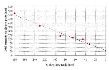
process technology nodes of 250 nanometer
250 nanometer
The 250 nm process refers to a level of semiconductor process technology.-Products featuring 250 nm manufacturing process:*The DEC Alpha 21264A, which was made commercially available in 1999.*The AMD K6-2 Chomper and Chomper Extended...
s and smaller. Older CMOS technologies and non-MOS technologies commonly use isolation based on LOCOS
LOCOS
LOCOS, short for LOCal Oxidation of Silicon, is a microfabrication process where silicon dioxide is formed in selected areas on a silicon wafer having the Si-SiO2 interface at a lower point than the rest of the silicon surface....
.
STI is created early during the semiconductor device fabrication process, before transistors are formed. The key steps of the STI process involve etching
Etching
Etching is the process of using strong acid or mordant to cut into the unprotected parts of a metal surface to create a design in intaglio in the metal...
a pattern of trenches in the silicon, depositing one or more dielectric
Dielectric
A dielectric is an electrical insulator that can be polarized by an applied electric field. When a dielectric is placed in an electric field, electric charges do not flow through the material, as in a conductor, but only slightly shift from their average equilibrium positions causing dielectric...
materials (such as silicon dioxide
Silicon dioxide
The chemical compound silicon dioxide, also known as silica , is an oxide of silicon with the chemical formula '. It has been known for its hardness since antiquity...
) to fill the trenches, and removing the excess dielectric using a technique such as chemical-mechanical planarization
Chemical-mechanical planarization
Chemical Mechanical Polishing/Planarization is a process of smoothing surfaces with the combination of chemical and mechanical forces. It can be thought of as a hybrid of chemical etching and free abrasive polishing.-Description:...
.http://smtbook.com/features.htm
Certain semiconductor fabrication technologies also include deep trench isolation, a related feature often found in analog integrated circuits
Analog chip
An analog chip is a set of miniature electronic analog circuits formed on a single piece of semiconductor material.-Description:The voltage and current at specified points in the circuits of an analog chips vary continuously in time. In contrast, digital chips only use and create voltages or...
.
The effect of the trench edge has given rise to what has recently been termed the "reverse narrow channel effect" or "inverse narrow width effect". Basically, due to the electric field
Electric field
In physics, an electric field surrounds electrically charged particles and time-varying magnetic fields. The electric field depicts the force exerted on other electrically charged objects by the electrically charged particle the field is surrounding...
enhancement at the edge, it is easier to form a conducting channel (by inversion) at a lower voltage. The threshold voltage
Threshold voltage
The threshold voltage of a MOSFET is usually defined as the gate voltage where an inversion layer forms at the interface between the insulating layer and the substrate of the transistor. The purpose of the inversion layer's forming is to allow the flow of electrons through the gate-source junction...
is effectively reduced for a narrower transistor width. The main concern for electronic devices is the resulting subthreshold leakage
Subthreshold leakage
The Subthreshold conduction or the subthreshold leakage or the subthreshold drain current is the current that flows between the source and drain of a MOSFET when the transistor is in subthreshold region, or weak-inversion region, that is, for gate-to-source voltages below the threshold voltage. The...
current, which is substantially larger after the threshold voltage reduction.
Process flow
- Stack deposition (oxide + protective nitride)
- Lithography print
- Dry etch
- Trench fill with oxide
- Chemical-mechanical polishing of the oxide
- Removal of the protective nitride
- Adjusting the oxide height to Si