
Dislocation
Encyclopedia
In materials science
, a dislocation is a crystallographic defect
, or irregularity, within a crystal structure
. The presence of dislocations strongly influences many of the properties of materials. The theory was originally developed by Vito Volterra
in 1905 but the term 'dislocation' was not coined until later by the late Professor Sir Frederick Charles Frank
of the Physics Department at the University of Bristol
.
Some types of dislocations can be visualized as being caused by the termination of a plane of atom
s in the middle of a crystal
. In such a case, the surrounding planes
are not straight, but instead bend around the edge of the terminating plane so that the crystal structure is perfectly ordered on either side. The analogy with a stack of paper is apt: if a half a piece of paper is inserted in a stack of paper, the defect in the stack is only noticeable at the edge of the half sheet.
There are two primary types: edge dislocations and screw dislocations. Mixed dislocations are intermediate between these.
 Mathematically, dislocations are a type of topological defect
, sometimes called a soliton
. The mathematical theory explains why dislocations behave as stable particles: they can be moved about, but maintain their identity as they move. Two dislocations of opposite orientation, when brought together, can cancel each other (this is the process of annihilation
), but a single dislocation typically cannot "disappear" on its own.
 Two main types of dislocation exist: edge and screw. Dislocations found in real materials typically are mixed, meaning that they have characteristics of both.
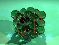
A crystalline material consists of a regular array of atoms, arranged into lattice planes (imagine stacking oranges in a grocery, each of the trays of oranges are the lattice planes). One approach is to begin by considering a 3-d representation of a perfect crystal lattice, with the atoms represented by spheres. The viewer may then start to simplify the representation by visualising planes of atoms instead of the atoms themselves (Figure A).
which describes the magnitude and direction of distortion to the lattice. In an edge dislocation, the Burgers vector is perpendicular to the line direction. (see also Jog (dislocations)
)
The stresses caused by an edge dislocation are complex due to its inherent asymmetry. These stresses are described by three equations:


where μ is the shear modulus of the material, b is the Burgers vector
, ν is Poisson's ratio
and x and y are coordinates.
These equations suggest a vertically oriented dumbbell of stresses surrounding the dislocation, with compression experienced by the atoms near the "extra" plane, and tension experienced by those atoms near the "missing" plane.
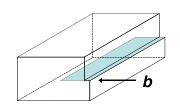
 A screw dislocation is much harder to visualize. Imagine cutting a crystal along a plane and slipping one half across the other by a lattice vector, the halves fitting back together without leaving a defect. If the cut only goes part way through the crystal, and then slipped, the boundary of the cut is a screw dislocation. It comprises a structure in which a helical path is traced around the linear defect (dislocation line) by the atomic planes in the crystal lattice (Figure C). Perhaps the closest analogy is a spiral-sliced ham. In pure screw dislocations, the Burgers vector is parallel to the line direction.
Despite the difficulty in visualization, the stresses caused by a screw dislocation are less complex than those of an edge dislocation. These stresses need only one equation, as symmetry allows only one radial coordinate to be used:

where μ is the shear modulus of the material, b is the Burgers vector, and r is a radial coordinate.
This equation suggests a long cylinder of stress radiating outward from the cylinder and decreasing with distance. Please note, this simple model results in an infinite value for the core of the dislocation at r=0 and so it is only valid for stresses outside of the core of the dislocation.
 When a dislocation line intersects the surface of a metallic material, the associated strain field locally increases the relative susceptibility of the material to acidic etching and an etch pit
of regular geometrical format results. If the material is strained (deformed) and repeatedly re-etched, a series of etch pits can be produced which effectively trace the movement of the dislocation in question.
Transmission electron microscopy
can be used to observe dislocations within the microstructure
of the material. Thin foils of metallic samples are prepared to render them transparent to the electron beam of the microscope. The electron
beam suffers diffraction
by the regular crystal lattice planes of the metal atoms and the differing relative angles between the beam and the lattice planes of each grain in the metal's microstructure result in image contrast (between grains of different crystallographic orientation). The less regular atomic structures of the grain boundaries and in the strain fields around dislocation lines have different diffractive properties than the regular lattice within the grains, and therefore present different contrast effects in the electron micrographs. (The dislocations are seen as dark lines in the lighter, central region of the micrographs on the right). Transmission electron micrographs of dislocations typically utilize magnifications of 50,000 to 300,000 times (though the equipment itself offers a wider range of magnifications than this).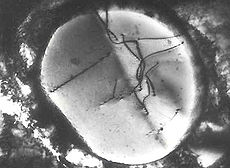 Some microscopes also permit the in-situ heating and/or deformation of samples, thereby permitting the direct observation of dislocation movement and their interactions. Note the characteristic 'wiggly' contrast of the dislocation lines as they pass through the thickness of the material. Note also that a dislocation cannot end within a crystal; the dislocation lines in these images end at the sample surface. A dislocation can only be contained within a crystal as a complete loop.
Field ion microscopy and atom probe
techniques offer methods of producing much higher magnifications (typically 3 million times and above) and permit the observation of dislocations at an atomic level. Where surface relief can be resolved to the level of an atomic step, screw dislocations appear as distinctive spiral features - thus revealing an important mechanism of crystal growth: where there is a surface step, atoms can more easily add to the crystal, and the surface step associated with a screw dislocation is never destroyed no matter how many atoms are added to it.
(By contrast, traditional optical microscopy, which is not appropriate for the direct observation of dislocations, typically offers magnifications up to a maximum of only around 2000 times).
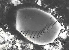
After chemical etching, small pits are formed where the etching solution preferentially attacks the sample surface around the dislocations intercepting this surface, due to the more highly strained state of the material . Thus, the image features indicate points at which dislocations intercept the sample surface. In this way, dislocations in silicon, for example, can be observed indirectly using an interference microscope. Crystal orientation can be determined by the shape of the etch pits associated with the dislocations (in the case of the illustration below; 100 elliptical, 111 - triangular/pyramidal).
 . Since the dislocation density increases with plastic deformation, a mechanism for the creation of dislocations must be activated in the material. Three mechanisms for dislocation formation are formed by homogeneous nucleation, grain boundary initiation, and interfaces the lattice and the surface, precipitates, dispersed phases, or reinforcing fibers.
The creation of a dislocation by homogeneous nucleation is a result of the rupture of the atomic bonds along a line in the lattice. A plane in the lattice is sheared, resulting in 2 oppositely faced half planes or dislocations. These dislocations move away from each other through the lattice. Since homogeneous nucleation forms dislocations from perfect crystals and requires the simultaneous breaking of many bonds, the energy required for homogeneous nucleation is high. For instance the stress required for homogeneous nucleation in copper has been shown to be , where G is the shear modulus of copper (46 GPa). Solving for
  , we see that the required stress is 3.4 GPa, which is very close to the theoretical strength of the crystal. Therefore, in conventional deformation homogeneous nucleation requires a concentrated stress, and is very unlikely. Grain boundary initiation and interface interaction are more common sources of dislocations.
Irregularities at the grain boundaries in materials can produce dislocations which propagate into the grain. The steps and ledges at the grain boundary are an important source of dislocations in the early stages of plastic deformation.
The surface of a crystal can produce dislocations in the crystal. Due to the small steps on the surface of most crystals, stress in certain regions on the surface is much larger than the average stress in the lattice. The dislocations are then propagated into the lattice in the same manner as in grain boundary initiation. In monocrystals, the majority of dislocations are formed at the surface. The dislocation density 200 micrometres into the surface of a material has been shown to be six times higher than the density in the bulk. However, in polycrystalline materials the surface sources cannot have a major effect because most grains are not in contact with the surface.
The interface between a metal and an oxide can greatly increase the number of dislocations created. The oxide layer puts the surface of the metal in tension because the oxygen atoms squeeze into the lattice, and the oxygen atoms are under compression. This greatly increases the stress on the surface of the metal and consequently the amount of dislocations formed at the surface. The increased amount of stress on the surface steps results in an increase of dislocations.
in microscopic terms. A naive attempt to calculate the shear stress
at which neighbouring atomic planes slip over each other in a perfect crystal suggests that, for a material with shear modulus G, shear strength τm is given approximately by:

As shear modulus in metal
s is typically within the range 20 000 to 150 000 MPa
, this is difficult to reconcile with shear stresses in the range 0.5 to 10 MPa observed to produce plastic deformation in experiments.
In 1934, Egon Orowan
, Michael Polanyi
and G. I. Taylor
, roughly simultaneously, realized that plastic deformation could be explained in terms of the theory of dislocations. Dislocations can move if the atoms from one of the surrounding planes break their bonds and rebond with the atoms at the terminating edge. In effect, a half plane of atoms is moved in response to shear stress by breaking and reforming a line of bonds, one (or a few) at a time. The energy required to break a single bond is far less than that required to break all the bonds on an entire plane of atoms at once. Even this simple model of the force required to move a dislocation shows that plasticity is possible at much lower stresses than in a perfect crystal. In many materials, particularly ductile materials, dislocations are the "carrier" of plastic deformation, and the energy required to move them is less than the energy required to fracture the material. Dislocations give rise to the characteristic malleability of metals.
When metals are subjected to "cold working" (deformation at temperatures which are relatively low as compared to the material's absolute melting temperature, Tm, i.e., typically less than 0.3 Tm) the dislocation density increases due to the formation of new dislocations and dislocation multiplication. The consequent increasing overlap between the strain fields of adjacent dislocations gradually increases the resistance to further dislocation motion. This causes a hardening of the metal as deformation progresses. This effect is known as strain hardening (also “work hardening”). Tangles of dislocations are found at the early stage of deformation and appear as non well-defined boundaries; the process of dynamic recovery
leads eventually to the formation of a cellular structure containing boundaries with misorientation lower than 15° (low angle grain boundaries). In addition, adding pinning points that inhibit the motion of dislocations, such as alloying elements, can introduce stress fields that ultimately strengthen the material by requiring a higher applied stress to overcome the pinning stress and continue dislocation motion.
The effects of strain hardening by accumulation of dislocations and the grain structure formed at high strain can be removed by appropriate heat treatment (annealing
) which promotes the recovery
and subsequent recrystallisation
of the material.
The combined processing techniques of work hardening
and annealing
allow for control over dislocation density, the degree of dislocation entanglement, and ultimately the yield strength of the material.
The driving force for dislocation climb is the movement of vacancies through a crystal lattice. If a vacancy moves next to the boundary of the extra half plane of atoms that forms an edge dislocation, the atom in the half plane closest to the vacancy can "jump" and fill the vacancy. This atom shift "moves" the vacancy in line with the half plane of atoms, causing a shift, or positive climb, of the dislocation. The process of a vacancy being absorbed at the boundary of a half plane of atoms, rather than created, is known as negative climb. Since dislocation climb results from individual atoms "jumping" into vacancies, climb occurs in single atom diameter increments.
During positive climb, the crystal shrinks in the direction perpendicular to the extra half plane of atoms because atoms are being removed from the half plane. Since negative climb involves an addition of atoms to the half plane, the crystal grows in the direction perpendicular to the half plane. Therefore, compressive stress in the direction perpendicular to the half plane promotes positive climb, while tensile stress promotes negative climb. This is one main difference between slip and climb, since slip is caused by only shear stress.
One additional difference between dislocation slip and climb is the temperature dependence. Climb occurs much more rapidly at high temperatures than low temperatures due to an increase in vacancy motion. Slip, on the other hand, has only a small dependence on temperature.
Materials science
Materials science is an interdisciplinary field applying the properties of matter to various areas of science and engineering. This scientific field investigates the relationship between the structure of materials at atomic or molecular scales and their macroscopic properties. It incorporates...
, a dislocation is a crystallographic defect
Crystallographic defect
Crystalline solids exhibit a periodic crystal structure. The positions of atoms or molecules occur on repeating fixed distances, determined by the unit cell parameters. However, the arrangement of atom or molecules in most crystalline materials is not perfect...
, or irregularity, within a crystal structure
Crystal structure
In mineralogy and crystallography, crystal structure is a unique arrangement of atoms or molecules in a crystalline liquid or solid. A crystal structure is composed of a pattern, a set of atoms arranged in a particular way, and a lattice exhibiting long-range order and symmetry...
. The presence of dislocations strongly influences many of the properties of materials. The theory was originally developed by Vito Volterra
Vito Volterra
Vito Volterra was an Italian mathematician and physicist, known for his contributions to mathematical biology and integral equations....
in 1905 but the term 'dislocation' was not coined until later by the late Professor Sir Frederick Charles Frank
Frederick Charles Frank
Sir Frederick Charles Frank FRS was a British theoretical physicist.He was born in Durban, South Africa, although his parents returned to England soon afterwards...
of the Physics Department at the University of Bristol
University of Bristol
The University of Bristol is a public research university located in Bristol, United Kingdom. One of the so-called "red brick" universities, it received its Royal Charter in 1909, although its predecessor institution, University College, Bristol, had been in existence since 1876.The University is...
.
Some types of dislocations can be visualized as being caused by the termination of a plane of atom
Atom
The atom is a basic unit of matter that consists of a dense central nucleus surrounded by a cloud of negatively charged electrons. The atomic nucleus contains a mix of positively charged protons and electrically neutral neutrons...
s in the middle of a crystal
Crystal
A crystal or crystalline solid is a solid material whose constituent atoms, molecules, or ions are arranged in an orderly repeating pattern extending in all three spatial dimensions. The scientific study of crystals and crystal formation is known as crystallography...
. In such a case, the surrounding planes
Plane (mathematics)
In mathematics, a plane is a flat, two-dimensional surface. A plane is the two dimensional analogue of a point , a line and a space...
are not straight, but instead bend around the edge of the terminating plane so that the crystal structure is perfectly ordered on either side. The analogy with a stack of paper is apt: if a half a piece of paper is inserted in a stack of paper, the defect in the stack is only noticeable at the edge of the half sheet.
There are two primary types: edge dislocations and screw dislocations. Mixed dislocations are intermediate between these.
Topological defect
In mathematics and physics, a topological soliton or a topological defect is a solution of a system of partial differential equations or of a quantum field theory homotopically distinct from the vacuum solution; it can be proven to exist because the boundary conditions entail the existence of...
, sometimes called a soliton
Soliton
In mathematics and physics, a soliton is a self-reinforcing solitary wave that maintains its shape while it travels at constant speed. Solitons are caused by a cancellation of nonlinear and dispersive effects in the medium...
. The mathematical theory explains why dislocations behave as stable particles: they can be moved about, but maintain their identity as they move. Two dislocations of opposite orientation, when brought together, can cancel each other (this is the process of annihilation
Annihilation
Annihilation is defined as "total destruction" or "complete obliteration" of an object; having its root in the Latin nihil . A literal translation is "to make into nothing"....
), but a single dislocation typically cannot "disappear" on its own.
Dislocation geometry
A crystalline material consists of a regular array of atoms, arranged into lattice planes (imagine stacking oranges in a grocery, each of the trays of oranges are the lattice planes). One approach is to begin by considering a 3-d representation of a perfect crystal lattice, with the atoms represented by spheres. The viewer may then start to simplify the representation by visualising planes of atoms instead of the atoms themselves (Figure A).
Edge dislocations
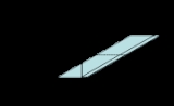
An edge dislocation is a defect where an extra half-plane of atoms is introduced mid way through the crystal, distorting nearby planes of atoms. When enough force is applied from one side of the crystal structure, this extra plane passes through planes of atoms breaking and joining bonds with them until it reaches the grain boundary. A simple schematic diagram of such atomic planes can be used to illustrate lattice defects such as dislocations. (Figure B represents the "extra half-plane" concept of an edge type dislocation). The dislocation has two properties, a line direction, which is the direction running along the bottom of the extra half plane, and the Burgers vectorBurgers vector
The Burgers vector, named after Dutch physicist Jan Burgers, is a vector, often denoted b, that represents the magnitude and direction of the lattice distortion of dislocation in a crystal lattice....
which describes the magnitude and direction of distortion to the lattice. In an edge dislocation, the Burgers vector is perpendicular to the line direction. (see also Jog (dislocations)
Jog (dislocations)
Jog is a term related to the concept of dislocation. It is used to describe the turns of a dislocation line inside a crystal structure. A dislocation line is rarely uniformly straight as in the figure, often containing many curves and/or steps to facilitate movement through the crystal in...
)
The stresses caused by an edge dislocation are complex due to its inherent asymmetry. These stresses are described by three equations:
where μ is the shear modulus of the material, b is the Burgers vector
Burgers vector
The Burgers vector, named after Dutch physicist Jan Burgers, is a vector, often denoted b, that represents the magnitude and direction of the lattice distortion of dislocation in a crystal lattice....
, ν is Poisson's ratio
Poisson's ratio
Poisson's ratio , named after Siméon Poisson, is the ratio, when a sample object is stretched, of the contraction or transverse strain , to the extension or axial strain ....
and x and y are coordinates.
These equations suggest a vertically oriented dumbbell of stresses surrounding the dislocation, with compression experienced by the atoms near the "extra" plane, and tension experienced by those atoms near the "missing" plane.
Screw dislocations
Despite the difficulty in visualization, the stresses caused by a screw dislocation are less complex than those of an edge dislocation. These stresses need only one equation, as symmetry allows only one radial coordinate to be used:
where μ is the shear modulus of the material, b is the Burgers vector, and r is a radial coordinate.
This equation suggests a long cylinder of stress radiating outward from the cylinder and decreasing with distance. Please note, this simple model results in an infinite value for the core of the dislocation at r=0 and so it is only valid for stresses outside of the core of the dislocation.
Mixed dislocations
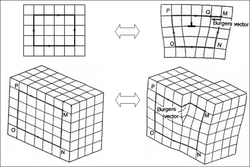
In many materials, dislocations are found where the line direction and Burgers vector are neither perpendicular nor parallel and these dislocations are called mixed dislocations, consisting of both screw and edge character.Observation of dislocations
Etch pit density
The etch pit density is a measure for the quality of semiconductor wafers. An etch solution is applied on the surface of the wafer where the etch rate is increased at dislocations of the crystal resulting in pits. For GaAs one uses typically molten KOH at 450 degrees Celsius for about 40 minutes...
of regular geometrical format results. If the material is strained (deformed) and repeatedly re-etched, a series of etch pits can be produced which effectively trace the movement of the dislocation in question.
Transmission electron microscopy
Transmission electron microscopy
Transmission electron microscopy is a microscopy technique whereby a beam of electrons is transmitted through an ultra thin specimen, interacting with the specimen as it passes through...
can be used to observe dislocations within the microstructure
Microstructure
Microstructure is defined as the structure of a prepared surface or thin foil of material as revealed by a microscope above 25× magnification...
of the material. Thin foils of metallic samples are prepared to render them transparent to the electron beam of the microscope. The electron
Electron
The electron is a subatomic particle with a negative elementary electric charge. It has no known components or substructure; in other words, it is generally thought to be an elementary particle. An electron has a mass that is approximately 1/1836 that of the proton...
beam suffers diffraction
Diffraction
Diffraction refers to various phenomena which occur when a wave encounters an obstacle. Italian scientist Francesco Maria Grimaldi coined the word "diffraction" and was the first to record accurate observations of the phenomenon in 1665...
by the regular crystal lattice planes of the metal atoms and the differing relative angles between the beam and the lattice planes of each grain in the metal's microstructure result in image contrast (between grains of different crystallographic orientation). The less regular atomic structures of the grain boundaries and in the strain fields around dislocation lines have different diffractive properties than the regular lattice within the grains, and therefore present different contrast effects in the electron micrographs. (The dislocations are seen as dark lines in the lighter, central region of the micrographs on the right). Transmission electron micrographs of dislocations typically utilize magnifications of 50,000 to 300,000 times (though the equipment itself offers a wider range of magnifications than this).
Field ion microscopy and atom probe
Atom probe
The atom probe is a microscope used in material science that was invented in 1967 by Erwin Wilhelm Müller, J. A. Panitz, and S. Brooks McLane. The atom probe is closely related to the method of Field Ion Microscopy, which is the first microscopic method to achieve atomic resolution, occurring in...
techniques offer methods of producing much higher magnifications (typically 3 million times and above) and permit the observation of dislocations at an atomic level. Where surface relief can be resolved to the level of an atomic step, screw dislocations appear as distinctive spiral features - thus revealing an important mechanism of crystal growth: where there is a surface step, atoms can more easily add to the crystal, and the surface step associated with a screw dislocation is never destroyed no matter how many atoms are added to it.
(By contrast, traditional optical microscopy, which is not appropriate for the direct observation of dislocations, typically offers magnifications up to a maximum of only around 2000 times).
After chemical etching, small pits are formed where the etching solution preferentially attacks the sample surface around the dislocations intercepting this surface, due to the more highly strained state of the material . Thus, the image features indicate points at which dislocations intercept the sample surface. In this way, dislocations in silicon, for example, can be observed indirectly using an interference microscope. Crystal orientation can be determined by the shape of the etch pits associated with the dislocations (in the case of the illustration below; 100 elliptical, 111 - triangular/pyramidal).
Sources of dislocations
Dislocation density in a material can be increased by plastic deformation by the following relationship:. Since the dislocation density increases with plastic deformation, a mechanism for the creation of dislocations must be activated in the material. Three mechanisms for dislocation formation are formed by homogeneous nucleation, grain boundary initiation, and interfaces the lattice and the surface, precipitates, dispersed phases, or reinforcing fibers.The creation of a dislocation by homogeneous nucleation is a result of the rupture of the atomic bonds along a line in the lattice. A plane in the lattice is sheared, resulting in 2 oppositely faced half planes or dislocations. These dislocations move away from each other through the lattice. Since homogeneous nucleation forms dislocations from perfect crystals and requires the simultaneous breaking of many bonds, the energy required for homogeneous nucleation is high. For instance the stress required for homogeneous nucleation in copper has been shown to be
, where G is the shear modulus of copper (46 GPa). Solving for , we see that the required stress is 3.4 GPa, which is very close to the theoretical strength of the crystal. Therefore, in conventional deformation homogeneous nucleation requires a concentrated stress, and is very unlikely. Grain boundary initiation and interface interaction are more common sources of dislocations.Irregularities at the grain boundaries in materials can produce dislocations which propagate into the grain. The steps and ledges at the grain boundary are an important source of dislocations in the early stages of plastic deformation.
The surface of a crystal can produce dislocations in the crystal. Due to the small steps on the surface of most crystals, stress in certain regions on the surface is much larger than the average stress in the lattice. The dislocations are then propagated into the lattice in the same manner as in grain boundary initiation. In monocrystals, the majority of dislocations are formed at the surface. The dislocation density 200 micrometres into the surface of a material has been shown to be six times higher than the density in the bulk. However, in polycrystalline materials the surface sources cannot have a major effect because most grains are not in contact with the surface.
The interface between a metal and an oxide can greatly increase the number of dislocations created. The oxide layer puts the surface of the metal in tension because the oxygen atoms squeeze into the lattice, and the oxygen atoms are under compression. This greatly increases the stress on the surface of the metal and consequently the amount of dislocations formed at the surface. The increased amount of stress on the surface steps results in an increase of dislocations.
Dislocations, slip and plasticity
Until the 1930s, one of the enduring challenges of materials science was to explain plasticityPlasticity (physics)
In physics and materials science, plasticity describes the deformation of a material undergoing non-reversible changes of shape in response to applied forces. For example, a solid piece of metal being bent or pounded into a new shape displays plasticity as permanent changes occur within the...
in microscopic terms. A naive attempt to calculate the shear stress
Shear stress
A shear stress, denoted \tau\, , is defined as the component of stress coplanar with a material cross section. Shear stress arises from the force vector component parallel to the cross section...
at which neighbouring atomic planes slip over each other in a perfect crystal suggests that, for a material with shear modulus G, shear strength τm is given approximately by:
As shear modulus in metal
Metal
A metal , is an element, compound, or alloy that is a good conductor of both electricity and heat. Metals are usually malleable and shiny, that is they reflect most of incident light...
s is typically within the range 20 000 to 150 000 MPa
MPA
-Academic degrees:* Master of Professional Accountancy* Master of Public Administration* Master of Public Affairs* Master of Physician's Assistant-Chemicals:* Medroxyprogesterone acetate, also known by the brand name Depo-Provera* Morpholide of pelargonic acid...
, this is difficult to reconcile with shear stresses in the range 0.5 to 10 MPa observed to produce plastic deformation in experiments.
In 1934, Egon Orowan
Egon Orowan
Egon Orowan was a Hungarian/British/U.S. physicist and metallurgist.-Life:Orowan was born in the Óbuda district of Budapest. His father, Berthold, was a mechanical engineer and factory manager, and his mother, Josze Spitzer Ságvári was the daughter of an impoverished land owner...
, Michael Polanyi
Michael Polanyi
Michael Polanyi, FRS was a Hungarian–British polymath, who made important theoretical contributions to physical chemistry, economics, and the theory of knowledge...
and G. I. Taylor
Geoffrey Ingram Taylor
Sir Geoffrey Ingram Taylor OM was a British physicist, mathematician and expert on fluid dynamics and wave theory. His biographer and one-time student, George Batchelor, described him as "one of the most notable scientists of this century".-Biography:Taylor was born in St. John's Wood, London...
, roughly simultaneously, realized that plastic deformation could be explained in terms of the theory of dislocations. Dislocations can move if the atoms from one of the surrounding planes break their bonds and rebond with the atoms at the terminating edge. In effect, a half plane of atoms is moved in response to shear stress by breaking and reforming a line of bonds, one (or a few) at a time. The energy required to break a single bond is far less than that required to break all the bonds on an entire plane of atoms at once. Even this simple model of the force required to move a dislocation shows that plasticity is possible at much lower stresses than in a perfect crystal. In many materials, particularly ductile materials, dislocations are the "carrier" of plastic deformation, and the energy required to move them is less than the energy required to fracture the material. Dislocations give rise to the characteristic malleability of metals.
When metals are subjected to "cold working" (deformation at temperatures which are relatively low as compared to the material's absolute melting temperature, Tm, i.e., typically less than 0.3 Tm) the dislocation density increases due to the formation of new dislocations and dislocation multiplication. The consequent increasing overlap between the strain fields of adjacent dislocations gradually increases the resistance to further dislocation motion. This causes a hardening of the metal as deformation progresses. This effect is known as strain hardening (also “work hardening”). Tangles of dislocations are found at the early stage of deformation and appear as non well-defined boundaries; the process of dynamic recovery
Recovery (metallurgy)
Recovery is a process by which deformed grains can reduce their stored energy by the removal or rearrangement of defects in their crystal structure. These defects, primarily dislocations, are introduced by plastic deformation of the material and act to increase the yield strength of a material...
leads eventually to the formation of a cellular structure containing boundaries with misorientation lower than 15° (low angle grain boundaries). In addition, adding pinning points that inhibit the motion of dislocations, such as alloying elements, can introduce stress fields that ultimately strengthen the material by requiring a higher applied stress to overcome the pinning stress and continue dislocation motion.
The effects of strain hardening by accumulation of dislocations and the grain structure formed at high strain can be removed by appropriate heat treatment (annealing
Annealing (metallurgy)
Annealing, in metallurgy and materials science, is a heat treatment wherein a material is altered, causing changes in its properties such as strength and hardness. It is a process that produces conditions by heating to above the recrystallization temperature, maintaining a suitable temperature, and...
) which promotes the recovery
Recovery (metallurgy)
Recovery is a process by which deformed grains can reduce their stored energy by the removal or rearrangement of defects in their crystal structure. These defects, primarily dislocations, are introduced by plastic deformation of the material and act to increase the yield strength of a material...
and subsequent recrystallisation
Recrystallization (metallurgy)
Recrystallization is a process by which deformed grains are replaced by a new set of undeformed grains that nucleate and grow until the original grains have been entirely consumed. Recrystallization is usually accompanied by a reduction in the strength and hardness of a material and a simultaneous...
of the material.
The combined processing techniques of work hardening
Work hardening
Work hardening, also known as strain hardening or cold working, is the strengthening of a metal by plastic deformation. This strengthening occurs because of dislocation movements within the crystal structure of the material. Any material with a reasonably high melting point such as metals and...
and annealing
Annealing (metallurgy)
Annealing, in metallurgy and materials science, is a heat treatment wherein a material is altered, causing changes in its properties such as strength and hardness. It is a process that produces conditions by heating to above the recrystallization temperature, maintaining a suitable temperature, and...
allow for control over dislocation density, the degree of dislocation entanglement, and ultimately the yield strength of the material.
Dislocation climb
Dislocations can slip in planes containing both the dislocation and the Burgers Vector. For a screw dislocation, the dislocation and the Burgers vector are parallel, so the dislocation may slip in any plane containing the dislocation. For an edge dislocation, the dislocation and the Burgers vector are perpendicular, so there is only one plane in which the dislocation can slip. There is an alternative mechanism of dislocation motion, fundamentally different from slip, that allows an edge dislocation to move out of its slip plane, known as dislocation climb. Dislocation climb allows an edge dislocation to move perpendicular to its slip plane.The driving force for dislocation climb is the movement of vacancies through a crystal lattice. If a vacancy moves next to the boundary of the extra half plane of atoms that forms an edge dislocation, the atom in the half plane closest to the vacancy can "jump" and fill the vacancy. This atom shift "moves" the vacancy in line with the half plane of atoms, causing a shift, or positive climb, of the dislocation. The process of a vacancy being absorbed at the boundary of a half plane of atoms, rather than created, is known as negative climb. Since dislocation climb results from individual atoms "jumping" into vacancies, climb occurs in single atom diameter increments.
During positive climb, the crystal shrinks in the direction perpendicular to the extra half plane of atoms because atoms are being removed from the half plane. Since negative climb involves an addition of atoms to the half plane, the crystal grows in the direction perpendicular to the half plane. Therefore, compressive stress in the direction perpendicular to the half plane promotes positive climb, while tensile stress promotes negative climb. This is one main difference between slip and climb, since slip is caused by only shear stress.
One additional difference between dislocation slip and climb is the temperature dependence. Climb occurs much more rapidly at high temperatures than low temperatures due to an increase in vacancy motion. Slip, on the other hand, has only a small dependence on temperature.
External links
- Defects in Crystals/ Prof. Dr. Helmut Föll website Chapter 5 contains a wealth of information on dislocations;
- DoITPoMS Online tutorial on dislocations, including movies of dislocations in bubble rafts;
- Scanning Tunneling Microscope - Gallery Image gallery, including a dislocations page, seen at the atomic level of metal surfaces, by the surface physics group at the Faculty of Physics, Vienna University of Technology, Austria.