
Atom probe
Encyclopedia
Erwin Wilhelm Müller
Erwin Wilhelm Müller was a German physicist who invented the Field Emission Electron Microscope , the Field Ion Microscope , and the Atom-Probe Field Ion Microscope...
, J. A. Panitz
J. A. Panitz
J. A. Panitz is the co-inventor of the Atom-Probe Field Ion Microscope and the inventor of the 10-cm atom-probe, the Imaging Atom-Probe, the LIFE detector , Isothermal Ramped Field-Desorption Spectroscopy , Field-Ion tomographyJ. A. Panitz is the co-inventor of the Atom-Probe Field Ion Microscope...
, and S. Brooks McLane
S. Brooks McLane
S. Brooks McLane co-invented the Atom-Probe Field Ion Microscope in 1967 along with J.A. Panitz and Erwin Wilhelm Müller. An electronics specialist and Professor of Physics, he co-authored the seminal "Field Absorption and desorption of helium and neon" that appeared in Surface Science in 1969...
. The atom probe is closely related to the method of Field Ion Microscopy, which is the first microscopic method to achieve atomic resolution, occurring in 1951.
Atom probes are unlike conventional optical or electron microscope
Electron microscope
An electron microscope is a type of microscope that uses a beam of electrons to illuminate the specimen and produce a magnified image. Electron microscopes have a greater resolving power than a light-powered optical microscope, because electrons have wavelengths about 100,000 times shorter than...
s, in that the magnification effect comes from the magnification provided by a highly curved electric field, rather than by the manipulation of radiation paths. Technically, the method is destructive in nature removing ions from a sample surface in order to image and identify them, generating magnifications sufficient to observe individual atoms as they are removed from the sample surface. Through coupling of this magnification method with time of flight mass spectrometry, ions evaporated by application of electric pulses can have their mass-to-charge ratio computed.
Through successive evaporation of material, layers of atoms are removed from a specimen, allowing for probing not only of the surface, but also through the material itself. Computer methods are utilised to rebuild a three dimensional view of the sample, prior to it being evaporated, providing atomic scale information on the structure of a sample, as well as providing the type atomic species information. The instrument allows the three-dimensional reconstruction of up to hundreds of millions of atom
Atom
The atom is a basic unit of matter that consists of a dense central nucleus surrounded by a cloud of negatively charged electrons. The atomic nucleus contains a mix of positively charged protons and electrically neutral neutrons...
s from a sharp tip (corresponding to specimen volumes of 10,000-1,000,000 nm3).
Overview
Atom probe samples are shaped to implicitly provide a highly curved electric potential to induce the resultant magnification, as opposed to direct use of lensing, such as via magnetic lensMagnetic lens
A magnetic lens is a device for the focusing or deflection of charged particles, such as electrons or ions. Charged particles are deflected based upon the strength of the magnetic field, which can be varied by controlling the current flowing through several electromagnets...
es. Furthermore, in normal operation (as opposed to a field ionization modes) the atom probe does not utilize a secondary source to probe the sample. Rather, the sample is evaporated in a controlled manner (field evaporation) and the evaporated ions are impacted onto a detector, which may be up to several meters from the specimen.
The samples used in atom probe are usually a metallic or semi-conducting material, with the needle geometry produced by electropolishing
Electropolishing
Electropolishing, also known as electrochemical polishing or electrolytic polishing , is an electrochemical process that removes material from a metallic workpiece. It is used to polish, passivate, and deburr metal parts. It is often described as the reverse of electroplating...
, or focused ion beam
Focused ion beam
Focused ion beam, also known as FIB, is a technique used particularly in the semiconductor industry, materials science and increasingly in the biological field for site-specific analysis, deposition, and ablation of materials. An FIB setup is a scientific instrument that resembles a scanning...
methods. Preparation is done, often by hand, to manufacture a tip radius sufficient to induce a high electric field, with radii on the order of 100 nm.
To conduct an atom probe experiment, such a needle is placed in an ultra high vacuum
Ultra high vacuum
Ultra-high vacuum is the vacuum regime characterised by pressures lower than about 10−7 pascal or 100 nanopascals . UHV requires the use of unusual materials in construction and by heating the entire system to 180°C for several hours to remove water and other trace gases which adsorb on the...
chamber. After introduction into the vacuum system, the sample is reduced to cryogenic temperatures (typically 20-100 K) and manipulated such that the needle's point is aimed towards an ion detector. A pulsed high voltage source (typically 1-2 kV) is generated and applied to the specimen, with pulse repetition rates in the hundreds of kilohertz range. The application of the pulsed voltage to the sample allows for individual ions at the sample surface to have their electric field, and hence atomic bonding, temporarily disrupted. This results in ejection of an ionised atom from the sample surface at a known time. The delay between application of the pulse and detection of the ion allows for the computation of a mass-to-charge ratio.
Whilst the uncertainty in the atomic mass computed by time-of-flight methods in atom probe is sufficiently small to allow for detection of individual isotopes within a material this uncertainty may still, in some cases, confound definitive identification of atomic species. Effects such as superposition of differing ions with multiple electrons removed, or through the presence of complex species formation during evaporation may cause two or more species to have sufficiently close time-of-flights to make definitive identification impossible.
Field Ion Microscopy
Field ion microscopy techniques were initially construed as a modification of field emissionField emission
Field emission is emission of electrons induced by an electrostatic field. The most common context is FE from a solid surface into vacuum. However, FE can take place from solid or liquid surfaces, into vacuum, air, a fluid, or any non-conducting or weakly-conducting dielectric...
, a technique which allows for a stream of electrons to be emitted from a sharp needle when subjected to a sufficiently high electric field (~3-6 V/nm). The needle is oriented towards a phosphor screen to create a projected image of the tip's work function
Work function
In solid-state physics, the work function is the minimum energy needed to remove an electron from a solid to a point immediately outside the solid surface...
, near the specimen surface. Whilst providing a projected image, the technique has limited resolution (2-2.5 nm), due to both quantum mechanical effects and lateral variation in electron velocity.
In field ion and atom probe methods, the polarity of the electric field is reversed, with a high positive field applied to the sample. For field ion microscopy a gas is introduced, known as the imaging gas, into the chamber at very low pressures. By application of a voltage during the presence of this gas, gas ions in the vicinity of the tip undergo ionisation, with greater numbers of ions generated immediately above atoms occupying edge or planar sites.
Imaging atom probe (IAP)
The imaging atom probe (IAP), invented in 1974 by J. A. PanitzJ. A. Panitz
J. A. Panitz is the co-inventor of the Atom-Probe Field Ion Microscope and the inventor of the 10-cm atom-probe, the Imaging Atom-Probe, the LIFE detector , Isothermal Ramped Field-Desorption Spectroscopy , Field-Ion tomographyJ. A. Panitz is the co-inventor of the Atom-Probe Field Ion Microscope...
, decreased the need to move the tip. In the IAP, ions emitted from the surface are recorded and mass analyzed at a detector placed within 12 cm of the tip (to provide a reasonably large field of view). By "time-gating" the detector for the arrival of a particular species of interest its crystallographic distribution on the surface, and as a function of depth, can be determined. Without time-gating all of the species reaching the detector are analyzed.
Atom-probe tomography (APT)
Atom-probe tomography (APT) uses a position-sensitive detector to deduce the lateral location of atoms. This allows 3-D reconstructions to be generated. The idea of the APT, inspired by J. A. Panitz's patent, was developed by Mike Miller starting in 1983 and culminated with the first prototype in 1986. Various refinements were made to the instrument, including the use of a so-called position-sensitive (PoS) detector by Alfred Cerezo, Terence Godfrey, and George D. W. Smith at Oxford University in 1988. The Tomographic Atom Probe (TAP), developed by researchers at the University of Rouen in France in 1993, introduced a multichannel timing system and multianode array. Both instruments (PoSAP and TAP) were commercialized by Oxford NanoscienceOxford Instruments
Oxford Instruments plc is a United Kingdom manufacturing and research company that designs and manufactures tools and systems for industry and research. The company is headquartered in Abingdon, Oxfordshire, England, with sites in the United Kingdom, United States, Europe, and Asia...
and Cameca
Cameca
Cameca is a manufacturer of scientific instruments, namely material analysis instruments based on Charged particle beam , ions or electrons- History :...
respectively. Since then, there have been many refinements to increase the field of view, mass and position resolution, and data acquisition rate of the instrument. In 2005, the commercialization of the pulsed laser atom probe (PLAP) expanded the avenues of research from highly conductive materials (metals) to poor conductors (semiconductors like silicon) and even insulating materials. AMETEK
AMETEK
AMETEK, Inc is a manufacturer of electronic instruments and electromechanical devices with headquarters in the United States and over 80 manufacturing sites worldwide....
acquired Cameca
Cameca
Cameca is a manufacturer of scientific instruments, namely material analysis instruments based on Charged particle beam , ions or electrons- History :...
in 2007 and Imago Scientific Instruments
Imago Scientific Instruments
Imago Scientific Instruments is a company founded in 1999 by Dr. Tom Kelly. At that time Tom Kelly was the Director of the Materials Science Center at the University of Wisconsin–Madison, but left his tenured position in 2001 to guide the company's growth...
(Madison, WI) in 2010, making the company the sole commercial developer of APTs.
Teeth of the radula
Radula
The radula is an anatomical structure that is used by molluscs for feeding, sometimes compared rather inaccurately to a tongue. It is a minutely toothed, chitinous ribbon, which is typically used for scraping or cutting food before the food enters the esophagus...
of chiton
Chiton
Chitons are small to large, primitive marine molluscs in the class Polyplacophora.There are 900 to 1,000 extant species of chitons in the class, which was formerly known as Amphineura....
Chaetopleura apiculata
Chaetopleura apiculata
Chaetopleura apiculata is a species of chiton in the family Chaetopleuridae. It is a marine mollusc.- Description :Teeth of the radula of this species has been studied by atom-probe tomography for the chemical structure and it have been published in 2011. It has been shown, that teeth contain...
has been studied by atom-probe tomography for the chemical structure and it have been published in 2011. It has been shown, that teeth contain fibres with surrounded by magnetite
Magnetite
Magnetite is a ferrimagnetic mineral with chemical formula Fe3O4, one of several iron oxides and a member of the spinel group. The chemical IUPAC name is iron oxide and the common chemical name is ferrous-ferric oxide. The formula for magnetite may also be written as FeO·Fe2O3, which is one part...
and some of them also with sodium
Sodium
Sodium is a chemical element with the symbol Na and atomic number 11. It is a soft, silvery-white, highly reactive metal and is a member of the alkali metals; its only stable isotope is 23Na. It is an abundant element that exists in numerous minerals, most commonly as sodium chloride...
or magnesium
Magnesium
Magnesium is a chemical element with the symbol Mg, atomic number 12, and common oxidation number +2. It is an alkaline earth metal and the eighth most abundant element in the Earth's crust and ninth in the known universe as a whole...
. It has been probably for the first time of using atom-probe tomography for the study of radula and in biominerals. This method can be used for example for further study of enamel
Tooth enamel
Tooth enamel, along with dentin, cementum, and dental pulp is one of the four major tissues that make up the tooth in vertebrates. It is the hardest and most highly mineralized substance in the human body. Tooth enamel is also found in the dermal denticles of sharks...
and dentin
Dentin
Dentine is a calcified tissue of the body, and along with enamel, cementum, and pulp is one of the four major components of teeth. Usually, it is covered by enamel on the crown and cementum on the root and surrounds the entire pulp...
of human teeth and bone
Bone
Bones are rigid organs that constitute part of the endoskeleton of vertebrates. They support, and protect the various organs of the body, produce red and white blood cells and store minerals. Bone tissue is a type of dense connective tissue...
s.
Field evaporation
Field evaporation is an effect that can occur when an atom bonded at the surface of a material is in the presence of a sufficiently high and appropriately directed electric field, where the electric field is the differential of electric potential (voltage) with respect to distance. Once this condition is met, it is sufficient that local bonding at the specimen surface is capable of being overcome by the field, allowing for evaporation of an atom from the surface to which it is otherwise bonded.Ion flight
Whether evaporated from the material itself, or ionised from the gas, the ions that are evaporated are accelerated by electrostatic force, acquiring most of their energy within a few tip-radii of the sample.Subsequently, the accelerative force on any given ion is controlled by the electrostatic equation, where n is the ionisation state of the ion, and e is the fundamental electric charge.

This can be equated with the mass of the ion, m, via Newton's law (F=ma):


Relativistic effects in the ion flight are usually ignored, as realisable ion speeds are only a very small fraction of the speed of light.
Assuming that the ion is accelerated during a very short interval, the ion can be assumed to be travelling at constant velocity. As the ion will travel from the tip at voltage V1 to some nominal ground potential, the speed at which the ion is travelling can be estimated by the energy transferred into the ion during (or near) ionisation. Therefore the ion speed can be computed with the following equation, which relates kinetic energy to energy gain due to the electric field.
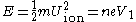
Where U is the ion velocity. Solving for U, the following relation is found:

For a singly charged hydrogen
Hydrogen
Hydrogen is the chemical element with atomic number 1. It is represented by the symbol H. With an average atomic weight of , hydrogen is the lightest and most abundant chemical element, constituting roughly 75% of the Universe's chemical elemental mass. Stars in the main sequence are mainly...
ion, ionised at 8 kV, the resulting velocity would be X ms−1. For a singly charged deuterium
Deuterium
Deuterium, also called heavy hydrogen, is one of two stable isotopes of hydrogen. It has a natural abundance in Earth's oceans of about one atom in of hydrogen . Deuterium accounts for approximately 0.0156% of all naturally occurring hydrogen in Earth's oceans, while the most common isotope ...
ion, the velocity would be Y ms−1. If a detector was placed at a distance of 1 m, the ion flight times would be X and Y ns. Thus, the time of the ion arrival can be used to infer the ion type itself, if the evaporation time is known.
From the above equation, it can be re-arranged to show that

given a known flight distance. F, for the ion, and a known flight time, t,

and thus one can substitute these values to obtain the mass-to-charge for the ion.

Thus for an ion which traverses a 1 m flight path, across a time of 2000 ns, given an initial accelerating voltage of 5000 V and noting that one amu is 1×10⁻²⁷ kg, the mass-to-charge ratio (more correctly the mass-to-ionisation value ratio) becomes Z amu/charge.
Magnification
The magnification in an atom is due to the projection of ions radially away from the small, sharp tip. Subsequently, in the far field, the ions will be greatly magnified. This magnification is sufficient to observe field variations due to individual atoms, thus allowing in field ion and field evaporation modes for the imaging of single atoms.The standard projection model for the atom probe is an emitter geometry that is based upon a revolution of a conic section
Conic section
In mathematics, a conic section is a curve obtained by intersecting a cone with a plane. In analytic geometry, a conic may be defined as a plane algebraic curve of degree 2...
, such as a sphere, hyperboloid or paraboloid
Paraboloid
In mathematics, a paraboloid is a quadric surface of special kind. There are two kinds of paraboloids: elliptic and hyperbolic. The elliptic paraboloid is shaped like an oval cup and can have a maximum or minimum point....
. For these tip models, solutions to the field may be approximated or obtained analytically. The magnification for a spherical emitter is inversely proportional to the radius of the tip, given a projection directly onto a spherical screen, the following equation can be obtained geometrically.

Where rscreen is the radius of the detection screen from the tip centre, and rtip the tip radius. Practical tip to screen distances may range from several centimeters to several meters, with increased detector area required at larger to subtend the same field of view
Field of view
The field of view is the extent of the observable world that is seen at any given moment....
.
Practically speaking, the usable magnification will be limited by several effects, such as lateral vibration of the atoms prior to evaporation.
Whilst the magnification of both the field ion and atom probe microscopes is extremely high, the exact magnification is dependant upon conditions specific to the examined specimen, so unlike for conventional electron microscope
Electron microscope
An electron microscope is a type of microscope that uses a beam of electrons to illuminate the specimen and produce a magnified image. Electron microscopes have a greater resolving power than a light-powered optical microscope, because electrons have wavelengths about 100,000 times shorter than...
s, there is often little direct control on magnification, and furthermore, obtained images may have strongly variable magnifications due to fluctuations in the shape of the electric field at the surface.
Reconstruction
The computational conversion of the ion sequence data, as obtained from a position sensitive detector, to a three dimensional visualisation of atomic types, is termed "reconstruction". Reconstruction algorithms are typically geometrically based, and have several literature formulations. Most models for reconstruction assume that the tip is a spherical object, and utilise empirical corrections to stereographic projectionStereographic projection
The stereographic projection, in geometry, is a particular mapping that projects a sphere onto a plane. The projection is defined on the entire sphere, except at one point — the projection point. Where it is defined, the mapping is smooth and bijective. It is conformal, meaning that it...
to convert detector positions back to a 2D surface embedded in R3. By sweeping this surface through R3 as a function of the ion sequence input data, such as via ion-ordering, a volume is generated onto which positions the 2D detector positions can be computed and placed three-dimensional space.
Typically the sweep takes the simple form of an advancement of the surface, such that the surface is expanded in a symmetric manner about its advancement axis, with the advancement rate set by some nominal volume attributed to each event, representative of the atomic volume of the atom prior to evaporation. This causes the final reconstructed volume to assume a rounded-conical shape, similar to a badminton shuttlecock
Shuttlecock
A shuttlecock, sometimes called a bird or birdie, is a high-drag projectile used in the sport of badminton. It has an open conical shape: the cone is formed from sixteen or so overlapping feathers, usually goose or duck and from the left wing only, embedded into a rounded cork base...
for . The detected events thus become a point cloud
Point cloud
A point cloud is a set of vertices in a three-dimensional coordinate system. These vertices are usually defined by X, Y, and Z coordinates, and typically are intended to be representative of the external surface of an object....
data with attributed experimentally measured values, such as ion time of flight or experimentally derived quantities, e.g. time of flight or detector data.
This form of data manipulation allows for rapid computer visualisation and analysis, with data presented as point cloud data with additional information, such as each ion's mass to charge (as computed from the velocity equation above), voltage or other auxiliary measured quantity or computation therefrom.
Data features
The canonical feature of atom probe data its high spatial resolution in the direction through the material, which has been attributed to an ordered evaporation sequence. This data can therefore image near atomically sharp interfaces with the associated chemical information.The data obtained from the evaporative process is however not without artefacts that form the physical evaporation or ionisation process. A key feature of the evaporation or field ion images is that the data density is highly inhomogeneous, due to the corrugation of the specimen surface at the atomic scale. This corrugation gives rise to strong electric field gradients in the near-tip zone (on the order of an atomic radii or less from the tip), which during ionisation deflects ions away from the electric field normal.
The resultant deflection means that in these regions of high curvature, atomic terraces are belied by a strong anisotropy in the detection density. Where this occurs due to a few atoms on a surface is usually referred to as a "pole", as these are coincident with the crystallographic axes of the specimen (FCC
Cubic crystal system
In crystallography, the cubic crystal system is a crystal system where the unit cell is in the shape of a cube. This is one of the most common and simplest shapes found in crystals and minerals....
, BCC
Cubic crystal system
In crystallography, the cubic crystal system is a crystal system where the unit cell is in the shape of a cube. This is one of the most common and simplest shapes found in crystals and minerals....
, HCP) etc. Where the edges of an atomic terrace causes deflection, a low density line is formed and is termed a "zone line".
These poles and zone-lines, whilst inducing fluctuations in data density in the reconstructed datasets, which can prove problematic during post-analysis, are critical for determining information such as angular magnification, as the crystallographic relationships between features are typically well known.
When reconstructing the data, owing to the evaporation of successive layers of material from the sample, the lateral and in-depth reconstruction values are highly anisotropic. Determination of the exact resolution of the instrument is of limited use, as the resolution of the device is set by the physical properties of the material under analysis.
Systems
Atom probe devices have only relatively recently been produced commercially, and many designs have been constructed since the method's inception. Initial field ion microscopes, precursors to modern atom probes, were usually glass blown devices developed by individual research laboratories.System layout
At a minimum, an atom probe will consist of several key pieces of equipment.- A vacuum system for maintaining the low pressures (~10−8 to 10−10 Pa) required.
- A system for manipulation of samples inside the vacuum, including sample viewing systems. Samples may be required to be cooled anywhere between room temperature to as low as 15 K.
- A cooling system to reduce atomic motion, such as a helium refrigeration circuit.
- A high voltage system to raise the sample voltage.
- A detection system for single ions for field evaporation.
Optionally, an atom probe may also include laser-optical systems for laser beam preparation, targeting and pulsing, if using laser-evaporation methods. Staged vacuum systems are regularly employed to ensure that the system vacuum conditions remain stable. In-situ reaction systems may also be employed for some studies.
Performance
Collectable ion volumes were previously limited to several thousand, or tens of thousands of ionic events. Subsequent electronics and instrumentation devleopment has increased the rate of data accumulation, with datasets of several tens of miillion atoms (dataset volumes of 105 nm3)Metallurgy
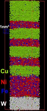
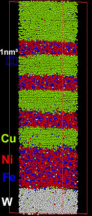
Atom probe has typically been employed in the chemical analysis of alloy systems at the atomic level. This has arisen as a result of voltage pulsed atom probes providing good chemical and sufficient spatial information in these materials. Metal samples from large grained alloys may be simple to fabricate, particularly from wire samples, with hand-electropolishing techniques giving good results.Subsequently, atom probe has been used in the analysis of the chemical composition of a wide range of alloys.
Such data is critical in determining the effeto of alloy constituents in a bulk material, identification of solid-state reaction features, such as solid phase precipitates. Such information may not be amenable to analysis by other means (e.g. TEM
Transmission electron microscopy
Transmission electron microscopy is a microscopy technique whereby a beam of electrons is transmitted through an ultra thin specimen, interacting with the specimen as it passes through...
) owing to the difficulty in generating a three dimensional dataset with composition.
Semiconductors
Semi-conductor materials are often analysable in atom probe, however sample preparation may be more difficult, and interpretation of results may be more complex, particularly if the semi-conductor contains phases which evaporate at differing electric field strengths.Applications such as ion implantation may be used to identify the distribution of dopants inside a semi-conducting material, which is increasingly critical in the correct design of modern nanometre scale electronics.
Limitations
- Materials implicitly control achievable, spatial resolution
- Specimen geometry is uncontrolled, yet controls projection behaviour, hence little control over the magnification. This may induce strong distortions into the computer generated 3D model dataset.
- Limited volume selectability, unlike EM methods. Site specific preparation methods, e.g. using Focussed ion beam preparation, although more time consuming, may be used to bypass such limitations.
- Features of interest may evaporate in a physically different manner to the bulk sample, altering projection geometry and the magnification of the reconstructed volume.
- Ion overlap in some samples (e.g. between oxygen and ) may result in ambiguous analysed species. This may be mitigated by selection of experiment temperature or laser input energy to influence the ionisation number (+, ++, 3+ etc.) of the ionised groups.
- Low molecular weight gases (Hydrogen & helium) may be difficult to remove from the analysis chamber, and may be adsorbed and emitted from the specimen, even though not present in the original specimen. This may also limit identification of Hydrogen in some samples. However deuterated samples have been used to overcome this limitation.
- Results may be contingent on the parameters used to convert the 2D detected data into 3D. Subsequently spatial measurements can be greatly affected, and careful analysis of the reconstructed volume is needd to ensure the correct results. In more problematic materials, correct reconstruction may be impossible due to limited knowledge of the true magnification; particularly if zone or pole regions cannot be observed.
External links
Americas
- Iowa State University
- Northwestern University Center for Atom-Probe Tomography
- Sandia National Laboratories
- The University of Alabama's Central Analytical Facility
- University of North Texas's Center for Advanced Research and Technology
- DOE's Environmental Molecular Sciences Laboratory