

Hybrid solar cell
Encyclopedia
Hybrid solar cells combine advantages of both organic
and inorganic semiconductors. Hybrid photovoltaics have organic materials that consist of conjugated polymers that absorb light as the donor and transport holes
. Inorganic materials in hybrid cell are used as the acceptor and electron
transporter in the structure. The hybrid photovoltaic devices have a significant potential for not only low-cost by roll-to-roll
processing but also scalable solar power conversion.
. Electrons in a solar cell absorb photon energy in sunlight, resulting in jumping to a conduction band
from a valence band
. This process generates a hole-electron pair
, which is separated by a potential barrier (such as p-n junction
), and induces a current flow.
 In hybrid solar cells, an organic material is mixed with a high electron transport material to form the photoactive layer. The two materials are assembled together in a heterojunction
type photoactive layer. By placing one material into contact with each other, the power conversion efficiency can be greater than a single material.
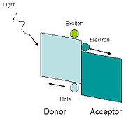
One of the materials acts as the photon absorber and exciton
donor, and the other facilitates exciton dissociation at the junction by charge transfer.
The steps for the charge transfer are:
The acceptor material needs a suitable energy offset to the binding energy of the exciton to the absorber. Charge transfer is favorable if the following condition is satisfied:

Where EA is the electron affinity and U is the coulombic binding energy of the exciton on the donor, and superscript A refers to the acceptor and superscript D refers to the donor. An energy diagram of the interface is shown in figure 1. In commonly used photovoltaic polymers such as MEH-PPV, the exciton binding energy ranges from 0.3 eV to 1.4 eV.
The energy required to separate the exciton is provided by the energy offset between the LUMOs
or conduction band of the donor and acceptor. After dissociation, the carriers are transported to the respective electrodes through a percolation network.
The average distance an exciton can diffuse through a material before annihilation by recombination happens is the exciton diffusion length. This is short in polymers, on the order of 5-10 nanometers. The time scale for radiative and non-radiative decay is from 1 picosecond to 1 nanosecond. Excitons generated within this length close to an acceptor would contribute to the photo current.
 To deal with the problem of the short exciton diffusion length, rather than a phase-separated bilayer, a bulk heterojunction structure is used. Dispersing the particles throughout the polymer matrix creates a larger interfacial area for charge transfer to occur. Figure 2 displays the difference between a bilayer and a bulk heterojunction.
There are several forms of controlling this nanoscale structure, with the main three being mesoporous inorganic films infused with electron-donating organic, alternatining inorganic-organic lamellar structures, and nanowire structures.
Mesoporous Films
Mesoporous films have been used a relatively high-efficiency hybrid solar cell. The structure of mesoporous thin film solar cells usually utilizes an inorganic, porous inorganic that is saturated with organic surfactant. The organic absorbs light, and transfers electrons to the inorganic-semiconductor (usually a transparent conducting oxide), which then transfers the electron to the electrode. Problems with these cells include their random ordering and the difficulty of controlling their nanoscale structure to promote charge conduction.
Order Lamellar Films
Recently, the use of alternating layers of organic and inorganic compounds have been controlled through electrodeposition-based self-assembly. These cells are of particular interest because it has been shown that the lamellar structure and periodicity of the alternating organic-inorganic layers can be controlled through solution chemistry. In order for these cells to be more efficient, however, larger organic surfactants that absorb more light in the visible spectrum must be deposited between the layers of electron-accepting inorganic so that their use is to be more practical.
Films of Ordered Nanostructures
Researchers have been able to grow nanostructure-based solar cells that use ordered nanostructures like nanowires or nanotubes of inorganic surrounding by electron-donating organics utilizing self-organization processes. Ordered nanostructures offer the advantage of directed charge transport and controlled phase separation between donor and acceptor materials. The nanowire-based morphology offers reduced internal reflection, facile strain relaxation and increased defect tolerance. The ability to make single-crystalline nanowires on low-cost substrates such as aluminum foil and to relax strain in subsequent layers removes two more major cost hurdles associated with high-efficiency cells. There have been rapid increases in efficiencies of nanowire-based solar cells and they seem to be one of the most promising nanoscale solar hybrid technologies.
Bandgap
Current organic photovoltaics have shown 70% of quantum efficiency for blue photons. However, the bandgap should be reduced to absorb red photons, which contains a significant fraction of the energy in the solar spectrum.
Interfaces
Contact resistance between each layer in the device should be minimized to offer higher fill factor and power conversion efficiency.
Charge transport
Higher charge carrier mobility allows the photovoltaics to have thicker active layers while photovoltaics minimize carrier recombination and keep the series resistance of the device low.
The photoactive layer can be created by mixing nanoparticles into a polymer matrix.
 For polymers used in this device, the hole mobilities are greater than electron mobilities, so the polymer phase is used to transport holes. The nanoparticles transport electrons to the electrode.
The interfacial area between the polymer phase and the nanoparticles needs to be large and this is achieved by dispersing the particles throughout the polymer matrix. However, the nanoparticles need to be interconnected to form percolation networks for electron transport, which occurs by hopping events.
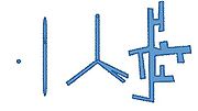
Aspect ratio, geometry, and volume fraction of the nanoparticles are factors in their efficiency. The structure of the nanoparticles can take a shape of a nanocrystal, nanorods, hyperbranched, and others. Figure 3 contains a picture of each structure. Implementing different structures changes the conversion efficiency in terms of nanoparticle dispersion in the polymer and providing pathways for electron transport.
The nanoparticle phase is required to provide a pathway for the electrons to reach the electrode. By using nanorods instead of nanocrystals, the hopping event from one crystal to another can be avoided.
Fabrication methods include mixing the two in a solution and spin-coating onto a substrate, and solvent evaporation (sol-gel). Most of these polymer fabrication methods do not involve high temperature processing. Annealing increases order in the polymer phase, increasing conductivity. However, annealing for too long would cause the polymer domain size to increase, eventually becoming larger than the exciton diffusion length, and possibly allowing some of the metal from the contact to diffuse into the photoactive layer, reducing the efficiency of the device.
level position and the ionization potential, which directly affects the open circuit voltage and the stability in air. The most common polymers used are P3HT (poly (3-hexylthiophene)), and M3H-PPV (poly[2-methoxy, 5-(2′-ethyl-hexyloxy)-p-phenylenevinylene)]). P3HT has a bandgap of 2.1 eV and M3H-PPV has a bandgap of around 2.4 eV. These values mesh with the bandgap of CdSe, which is 2.10 eV. The electron affinity of CdSe ranges from 4.4 to 4.7 eV. If the polymer used was MEH-PPV which has an electron affinity of 3.0 eV, the difference between the two is large enough to drive electron transfer from the CdSe to the polymer. CdSe also has a high electron mobility of 600 cm2/(V·s).
derivate as the polymer and CdSe tetropods as the nanoparticle phase has an open circuit voltage of 0.76 V, a short circuit current of 6.42 mA/cm2, a fill factor of 0.44, and a power conversion efficiency of 2.4%.
Problems include controlling the amount of nanoparticle aggregation as the photolayer forms. The particles need to be dispersed in order to maximize interface area, but need to aggregate to form networks for electron transport. The network formation is sensitive to the fabrication conditions. Dead end pathways can impede flow. A possible solution is implementing ordered heterojunctions, where the structure is well controlled.
The structures can undergo morphological changes over time, namely phase separation. Eventually, the polymer domain size will be greater than the carrier diffusion length, which lowers performance.
Even though the nanoparticle bandgap can be tuned, it needs to be matched with the corresponding polymer. The 2.0 eV bandgap of CdSe is larger than an ideal bandgap of 1.4 for absorbance of light.
Compared to bulk silicon semiconductors, the properties of these structures are lacking. The carrier mobilities are much smaller than that of silicon. Electron in silicon is 1000 cm2/(V·s) while in CdSe it’s 600 cm2/(V·s), and other quantum dot materials is less than 10 cm2/(V·s). Hole mobility in MEH-PPV is 0.1 cm2/(V·s), while in silicon it is 450 cm2/(V·s).
s (CNTs) have high electron conductivity, high thermal conductivity, robustness, and are flexible by nature. Field emission displays (FED), strain sensors, field effect transistor (FET) have been demonstrated. Each application shows the potential of CNT for nanoscale devices and for flexible electronics applications. Photovoltaic applications have also been explored for this novel material.
Mainly, CNT have been utilized as either the photo-induced exciton carrier transport medium impurity within a polymer-based photovoltaic layer or as the photoactive (photon-electron conversion) layer. The metallic CNT is preferred for the former application, while semiconducting CNT is preferred for the later.
 To increase the photovoltaic efficiency, electron accepting impurities must be added within the photoactive region. Thus, by incorporating CNT within the polymer, dissociation of the exciton pair can be accomplished by the CNT matrix. The high surface area (~1600 m2/g) of CNT offers a tremendous opportunity for exciton dissociation. The separated carriers within the polymer-CNT matrix are transported by the percolation pathways of adjacent CNTs, providing the means for high carrier mobility and efficient charge transfer. The factors of performance of CNT-polymer hybrid photovoltaic are low compared to inorganic photovoltaic. SWNT in P3OT semiconductor polymer demonstrated open circuit voltage (Voc) is under 0.94 V, with short circuit current (Isc) of 0.12 mA/cm2.
Metal nanoparticles may be applied to the exterior of CNT to increase the exciton separation efficiency. The metal provides a higher electric field at the CNT-polymer interface, hence accelerating the exciton carriers to be more effectively transferred to the CNT matrix. In this case, Voc is 0.3396 V, with Isc to be 5.88 mA/cm2. The fill factor is 0.3876%, with the white light conversion factor being 0.775%.
A strong built-in electric field in SWNT for efficient photogenerated electron-hole pair separation has been demonstrated by using two asymmetrical metal electrodes with high and low work functions. The open circuit voltage (Voc) is 0.28 V, with short circuit current (Isc) of 1.12 nA/cm2, with an incident light source of 8.8 W/cm2. The resulting white light conversion factor is 0.8%.
Challenges as efficient carrier transport medium
Additional challenges involve the dispersion of CNT within the polymer photoactive layer. The CNT is required to be well dispersed within the polymer matrix to form efficient pathways between the occurrence of the excitons and the electrode. Failure to do so will result in inefficient charge transfer.
Challenges as photoactive matrix layer
Challenges of CNT for the photoactive layer include the lack of capability to form a p-n junction
. The latter results in an internal built-in potential, providing pathway for efficient carrier separation within the photovoltaic. It is extremely difficult to dope certain segments of a CNT, hence the formation of PN junction has not been demonstrated thus far. To overcome this difficulty, energy band bending has been done by the use of two electrodes having different work functions. A strong built-in electric field covering the whole SWNT channel is formed for high-efficiency carrier separation. Also, oxidation issue of CNT is more critical for this application. Oxidized CNT have a tendency to become more metallic, losing merit as a photovoltaic material.
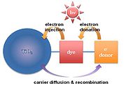 TiO2 nanoparticles are synthesized in several tens of nanometer scales (~100 nm). In order to make a photovoltaic cell, molecular sensitizers (dye molecules) are attached to the titania surface. The dye-absorbed titania is finally enclosed by a liquid electrolyte. This type of dye-sensitized solar cell is also known as a Grätzel cell. Dye-sensitized solar cell has a disadvantage of a short diffusion length. Recently, supermolecular or multifunctional sensitizers have been investigated so as to enhance carrier diffusion length. For example, a dye chromophore
has been modified by the addition of secondary electron donors. Minority carriers (holes in this case) diffuse to the attached electron donors to recombine. Therefore, electron-hole recombination is retarded by the physical separation between the dye–cation moiety and the TiO2 surface, as shown in Fig. 5. Finally, this process raises the carrier diffusion length, resulting in the increase of carrier lifetime.
Mesoporous materials contain pores with diameters between 2 and 50 nm. A dye-sensitized mesoporous film of TiO2 can be used for making photovoltaic cells and this solar cell is called a ‘solid-state dye sensitized solar cell’. The pores in mesoporous TiO2 thin film are filled with a solid hole-conducting material such as p-type semiconductors or organic hole conducting material. Replacing the liquid electrolyte in Grätzel’s cells with a solid charge-transport material can be beneficial. The process of electron-hole generation and recombination is the same as Grätzel cells. Electrons are injected from photoexcited dye into the conduction band of titania and holes are transported by a solid charge transport electrolyte to an electrode. Many organic materials have been tested to obtain a high solar-to-energy conversion efficiency in dye synthesized solar cells based on mesoporous titania thin film.
For solid-state dye sensitized solar cells, first challenge originates from disordered titania mesoporous structures. Mesoporous titnaia structures should be fabricated with well-ordered titania structures in uniform size (~ 10 nm). Second challenge comes from solid electrolyte. To develop the solid electrolyte, several requirements should be considered. The solid electrolyte is required to have special properties:
Although this system has not yet been incorporated into a photovoltaic device, preliminary photoconductivity measurements have shown that this system exhibits among the highest values measured for organic, hybrid, and amorphous silicon photoconductors, and so, offers promise in creating efficient hybrid photovoltaic devices.
Organic semiconductor
An organic semiconductor is an organic material with semiconductor properties. Single molecules, short chain and organic polymers can be semiconductive. Semiconducting small molecules include the polycyclic aromatic compounds pentacene, anthracene, and rubrene...
and inorganic semiconductors. Hybrid photovoltaics have organic materials that consist of conjugated polymers that absorb light as the donor and transport holes
Electron hole
An electron hole is the conceptual and mathematical opposite of an electron, useful in the study of physics, chemistry, and electrical engineering. The concept describes the lack of an electron at a position where one could exist in an atom or atomic lattice...
. Inorganic materials in hybrid cell are used as the acceptor and electron
Electron
The electron is a subatomic particle with a negative elementary electric charge. It has no known components or substructure; in other words, it is generally thought to be an elementary particle. An electron has a mass that is approximately 1/1836 that of the proton...
transporter in the structure. The hybrid photovoltaic devices have a significant potential for not only low-cost by roll-to-roll
Roll-to-roll processing
In the field of electronic devices, Roll-to-roll processing, also known as web processing, reel-to-reel processing or R2R, is the process of creating electronic devices on a roll of flexible plastic or metal foil...
processing but also scalable solar power conversion.
Solar cell
Solar cells are devices that convert sunlight directly into electricity by the photovoltaic effectPhotovoltaic effect
The photovoltaic effect is the creation of voltage or electric current in a material upon exposure to light. Though the photovoltaic effect is directly related to the photoelectric effect, they are different processes. In the photoelectric effect, electrons are ejected from a material's surface...
. Electrons in a solar cell absorb photon energy in sunlight, resulting in jumping to a conduction band
Conduction band
In the solid-state physics field of semiconductors and insulators, the conduction band is the range of electron energies, higher than that of the valence band, sufficient to free an electron from binding with its individual atom and allow it to move freely within the atomic lattice of the material...
from a valence band
Valence band
In solids, the valence band is the highest range of electron energies in which electrons are normally present at absolute zero temperature....
. This process generates a hole-electron pair
Exciton
An exciton is a bound state of an electron and hole which are attracted to each other by the electrostatic Coulomb force. It is an electrically neutral quasiparticle that exists in insulators, semiconductors and some liquids...
, which is separated by a potential barrier (such as p-n junction
P-n junction
A p–n junction is formed at the boundary between a P-type and N-type semiconductor created in a single crystal of semiconductor by doping, for example by ion implantation, diffusion of dopants, or by epitaxy .If two separate pieces of material were used, this would...
), and induces a current flow.
Organic solar cell
Organic solar cells use organic materials in the active layer of the devices. Molecular, polymer, and hybrid organic photovoltaics are the main kinds of organic photovoltaic devices that are currently studied.Hybrid solar cell
Heterojunction
A heterojunction is the interface that occurs between two layers or regions of dissimilar crystalline semiconductors. These semiconducting materials have unequal band gaps as opposed to a homojunction...
type photoactive layer. By placing one material into contact with each other, the power conversion efficiency can be greater than a single material.
One of the materials acts as the photon absorber and exciton
Exciton
An exciton is a bound state of an electron and hole which are attracted to each other by the electrostatic Coulomb force. It is an electrically neutral quasiparticle that exists in insulators, semiconductors and some liquids...
donor, and the other facilitates exciton dissociation at the junction by charge transfer.
The steps for the charge transfer are:
- Excitation on donor
- Excitation delocalized on a donor-acceptor complex
- Charge-transfer initiated.
- Charge separation.
The acceptor material needs a suitable energy offset to the binding energy of the exciton to the absorber. Charge transfer is favorable if the following condition is satisfied:
Where EA is the electron affinity and U is the coulombic binding energy of the exciton on the donor, and superscript A refers to the acceptor and superscript D refers to the donor. An energy diagram of the interface is shown in figure 1. In commonly used photovoltaic polymers such as MEH-PPV, the exciton binding energy ranges from 0.3 eV to 1.4 eV.
The energy required to separate the exciton is provided by the energy offset between the LUMOs
HOMO/LUMO
HOMO and LUMO are acronyms for highest occupied molecular orbital and lowest unoccupied molecular orbital, respectively. The energy difference between the HOMO and LUMO is termed the HOMO-LUMO gap...
or conduction band of the donor and acceptor. After dissociation, the carriers are transported to the respective electrodes through a percolation network.
The average distance an exciton can diffuse through a material before annihilation by recombination happens is the exciton diffusion length. This is short in polymers, on the order of 5-10 nanometers. The time scale for radiative and non-radiative decay is from 1 picosecond to 1 nanosecond. Excitons generated within this length close to an acceptor would contribute to the photo current.
Types of Interfaces and Structures
Controlling the interface of inorganic-orgnaic hybrid solar cells can increase the efficiency of the cells. This increased efficiency can be achieved by increasing the interfacial surface area between the organic and the inorganic to facilitate charge separation and by controlling the nanoscale lengths and periodicity of each structure so that charges are allowed to separate and move toward the appropriate electrode without recombining.There are several forms of controlling this nanoscale structure, with the main three being mesoporous inorganic films infused with electron-donating organic, alternatining inorganic-organic lamellar structures, and nanowire structures.
Mesoporous Films
Mesoporous films have been used a relatively high-efficiency hybrid solar cell. The structure of mesoporous thin film solar cells usually utilizes an inorganic, porous inorganic that is saturated with organic surfactant. The organic absorbs light, and transfers electrons to the inorganic-semiconductor (usually a transparent conducting oxide), which then transfers the electron to the electrode. Problems with these cells include their random ordering and the difficulty of controlling their nanoscale structure to promote charge conduction.
Order Lamellar Films
Recently, the use of alternating layers of organic and inorganic compounds have been controlled through electrodeposition-based self-assembly. These cells are of particular interest because it has been shown that the lamellar structure and periodicity of the alternating organic-inorganic layers can be controlled through solution chemistry. In order for these cells to be more efficient, however, larger organic surfactants that absorb more light in the visible spectrum must be deposited between the layers of electron-accepting inorganic so that their use is to be more practical.
Films of Ordered Nanostructures
Researchers have been able to grow nanostructure-based solar cells that use ordered nanostructures like nanowires or nanotubes of inorganic surrounding by electron-donating organics utilizing self-organization processes. Ordered nanostructures offer the advantage of directed charge transport and controlled phase separation between donor and acceptor materials. The nanowire-based morphology offers reduced internal reflection, facile strain relaxation and increased defect tolerance. The ability to make single-crystalline nanowires on low-cost substrates such as aluminum foil and to relax strain in subsequent layers removes two more major cost hurdles associated with high-efficiency cells. There have been rapid increases in efficiencies of nanowire-based solar cells and they seem to be one of the most promising nanoscale solar hybrid technologies.
Fundamental challenge factors
In order to start large-scale manufacturing, the efficiency must be higher. There are three factors that must be considered: 1) bandgap, 2) interfaces, and 3) charge transport.Bandgap
Current organic photovoltaics have shown 70% of quantum efficiency for blue photons. However, the bandgap should be reduced to absorb red photons, which contains a significant fraction of the energy in the solar spectrum.
Interfaces
Contact resistance between each layer in the device should be minimized to offer higher fill factor and power conversion efficiency.
Charge transport
Higher charge carrier mobility allows the photovoltaics to have thicker active layers while photovoltaics minimize carrier recombination and keep the series resistance of the device low.
Polymer–nanoparticle composite
Nanoparticles are a class of semiconductor materials whose size in at least one dimension ranges from 1 to 100 nanometers, on the order of exciton wavelengths. This size control creates quantum confinement and allows for the tuning of optoelectronic properties, such as band gap and electron affinity. Nanoparticles also have a large surface area to volume ratio, which presents more area for charge transfer to occur.The photoactive layer can be created by mixing nanoparticles into a polymer matrix.
Structure and processing
The interfacial area between the polymer phase and the nanoparticles needs to be large and this is achieved by dispersing the particles throughout the polymer matrix. However, the nanoparticles need to be interconnected to form percolation networks for electron transport, which occurs by hopping events.
Aspect ratio, geometry, and volume fraction of the nanoparticles are factors in their efficiency. The structure of the nanoparticles can take a shape of a nanocrystal, nanorods, hyperbranched, and others. Figure 3 contains a picture of each structure. Implementing different structures changes the conversion efficiency in terms of nanoparticle dispersion in the polymer and providing pathways for electron transport.
The nanoparticle phase is required to provide a pathway for the electrons to reach the electrode. By using nanorods instead of nanocrystals, the hopping event from one crystal to another can be avoided.
Fabrication methods include mixing the two in a solution and spin-coating onto a substrate, and solvent evaporation (sol-gel). Most of these polymer fabrication methods do not involve high temperature processing. Annealing increases order in the polymer phase, increasing conductivity. However, annealing for too long would cause the polymer domain size to increase, eventually becoming larger than the exciton diffusion length, and possibly allowing some of the metal from the contact to diffuse into the photoactive layer, reducing the efficiency of the device.
Materials
Inorganic semiconductor nanoparticles used in hybrid cells include CdSe (size ranges from 6-20 nm), ZnO, TiO, and PbS. Common polymers used as photo materials have extensive conjugation and also happen to be hydrophobic. Their efficiency as a photo material is affected by the HOMOHOMO/LUMO
HOMO and LUMO are acronyms for highest occupied molecular orbital and lowest unoccupied molecular orbital, respectively. The energy difference between the HOMO and LUMO is termed the HOMO-LUMO gap...
level position and the ionization potential, which directly affects the open circuit voltage and the stability in air. The most common polymers used are P3HT (poly (3-hexylthiophene)), and M3H-PPV (poly[2-methoxy, 5-(2′-ethyl-hexyloxy)-p-phenylenevinylene)]). P3HT has a bandgap of 2.1 eV and M3H-PPV has a bandgap of around 2.4 eV. These values mesh with the bandgap of CdSe, which is 2.10 eV. The electron affinity of CdSe ranges from 4.4 to 4.7 eV. If the polymer used was MEH-PPV which has an electron affinity of 3.0 eV, the difference between the two is large enough to drive electron transfer from the CdSe to the polymer. CdSe also has a high electron mobility of 600 cm2/(V·s).
Performance values
Values demonstrated for a cell with a PPVPoly(p-phenylene vinylene)
Poly is a conducting polymer of the rigid-rod polymer host family.PPV is the only polymer of this type that has so far been successfully processed into a highly ordered crystalline thin film. PPV and its derivatives are conducting polymers of rigid-rod polymer family...
derivate as the polymer and CdSe tetropods as the nanoparticle phase has an open circuit voltage of 0.76 V, a short circuit current of 6.42 mA/cm2, a fill factor of 0.44, and a power conversion efficiency of 2.4%.
Challenges
These structures need increased efficiency values and good stability over time before commercialization is feasible. Silicon photodevices has power conversion efficiencies greater than 20%, much greater than the 2.4% of the CdSe-PPV system.Problems include controlling the amount of nanoparticle aggregation as the photolayer forms. The particles need to be dispersed in order to maximize interface area, but need to aggregate to form networks for electron transport. The network formation is sensitive to the fabrication conditions. Dead end pathways can impede flow. A possible solution is implementing ordered heterojunctions, where the structure is well controlled.
The structures can undergo morphological changes over time, namely phase separation. Eventually, the polymer domain size will be greater than the carrier diffusion length, which lowers performance.
Even though the nanoparticle bandgap can be tuned, it needs to be matched with the corresponding polymer. The 2.0 eV bandgap of CdSe is larger than an ideal bandgap of 1.4 for absorbance of light.
Compared to bulk silicon semiconductors, the properties of these structures are lacking. The carrier mobilities are much smaller than that of silicon. Electron in silicon is 1000 cm2/(V·s) while in CdSe it’s 600 cm2/(V·s), and other quantum dot materials is less than 10 cm2/(V·s). Hole mobility in MEH-PPV is 0.1 cm2/(V·s), while in silicon it is 450 cm2/(V·s).
Carbon nanotubes
Carbon nanotubeCarbon nanotube
Carbon nanotubes are allotropes of carbon with a cylindrical nanostructure. Nanotubes have been constructed with length-to-diameter ratio of up to 132,000,000:1, significantly larger than for any other material...
s (CNTs) have high electron conductivity, high thermal conductivity, robustness, and are flexible by nature. Field emission displays (FED), strain sensors, field effect transistor (FET) have been demonstrated. Each application shows the potential of CNT for nanoscale devices and for flexible electronics applications. Photovoltaic applications have also been explored for this novel material.
Mainly, CNT have been utilized as either the photo-induced exciton carrier transport medium impurity within a polymer-based photovoltaic layer or as the photoactive (photon-electron conversion) layer. The metallic CNT is preferred for the former application, while semiconducting CNT is preferred for the later.
Efficient carrier transport medium
Metal nanoparticles may be applied to the exterior of CNT to increase the exciton separation efficiency. The metal provides a higher electric field at the CNT-polymer interface, hence accelerating the exciton carriers to be more effectively transferred to the CNT matrix. In this case, Voc is 0.3396 V, with Isc to be 5.88 mA/cm2. The fill factor is 0.3876%, with the white light conversion factor being 0.775%.
Photoactive matrix layer
CNT may be used as a photovoltaic device not only as an add-in material to increase carrier transport, but also as the photoactive layer itself. The semiconducting single walled CNT (SWCNT) is a potentially attractive material for photovoltaic applications for the unique structural and electrical properties. SWCNT has high electric conductivity (100 times that of copper) and show ballistic carrier transport, greatly decreasing carrier recombination. Bandgap of the SWCNT is inversely proportional to the tube diameter. Hence this single material may show multiple direct bandgaps matching the solar spectrum.A strong built-in electric field in SWNT for efficient photogenerated electron-hole pair separation has been demonstrated by using two asymmetrical metal electrodes with high and low work functions. The open circuit voltage (Voc) is 0.28 V, with short circuit current (Isc) of 1.12 nA/cm2, with an incident light source of 8.8 W/cm2. The resulting white light conversion factor is 0.8%.
Challenges
Several challenges must be addressed for CNT to be used in photovoltaic applications. CNT degrades overtime in oxygen rich environment. The passivation layer required to prevent CNT oxidation may reduce the optical transparency of the electrode region, hence lowering the photovoltaic efficiency.Challenges as efficient carrier transport medium
Additional challenges involve the dispersion of CNT within the polymer photoactive layer. The CNT is required to be well dispersed within the polymer matrix to form efficient pathways between the occurrence of the excitons and the electrode. Failure to do so will result in inefficient charge transfer.
Challenges as photoactive matrix layer
Challenges of CNT for the photoactive layer include the lack of capability to form a p-n junction
P-n junction
A p–n junction is formed at the boundary between a P-type and N-type semiconductor created in a single crystal of semiconductor by doping, for example by ion implantation, diffusion of dopants, or by epitaxy .If two separate pieces of material were used, this would...
. The latter results in an internal built-in potential, providing pathway for efficient carrier separation within the photovoltaic. It is extremely difficult to dope certain segments of a CNT, hence the formation of PN junction has not been demonstrated thus far. To overcome this difficulty, energy band bending has been done by the use of two electrodes having different work functions. A strong built-in electric field covering the whole SWNT channel is formed for high-efficiency carrier separation. Also, oxidation issue of CNT is more critical for this application. Oxidized CNT have a tendency to become more metallic, losing merit as a photovoltaic material.
Dye-sensitized
Dye-sensitized solar cells consists of a photo-sensitized anode, an electrolyte, and a photo-electrochemical system. Hybrid solar cells based on dye-sensitized solar cells are formed with inorganic materials (TiO2) and organic materials.Materials
Hybrid solar cells based on dye-sensitized solar cells are fabricated by dye-absorbed inorganic materials and organic materials. TiO2 is the preferred inorganic material since this material is easy to synthesize and acts as a n-type semiconductor due to the donor-like oxygen vacancies. However, titania only absorbs a small fraction of the UV spectrum. Molecular sensitizers (dye molecules) attached to the semiconductor surface are used to collect a greater portion of the spectrum. In the case of titania dye-sensitized solar cells, a photon absorbed by a dye-sensitizer molecule layer induces electron injection into the conduction band of titania, resulting in current flow. However, short diffusion length (diffusivity, Dn≤10−4cm2/s) in titania dye-sensitized solar cells decrease the solar-to-energy conversion efficiency. To enhance diffusion length (or carrier lifetime), a variety of organic materials are attached to the titania.Dye-sensitized photoelectrochemical cell (Grätzel cell)
Chromophore
A chromophore is the part of a molecule responsible for its color. The color arises when a molecule absorbs certain wavelengths of visible light and transmits or reflects others. The chromophore is a region in the molecule where the energy difference between two different molecular orbitals falls...
has been modified by the addition of secondary electron donors. Minority carriers (holes in this case) diffuse to the attached electron donors to recombine. Therefore, electron-hole recombination is retarded by the physical separation between the dye–cation moiety and the TiO2 surface, as shown in Fig. 5. Finally, this process raises the carrier diffusion length, resulting in the increase of carrier lifetime.
Solid-state dye sensitized solar cell
Mesoporous materials contain pores with diameters between 2 and 50 nm. A dye-sensitized mesoporous film of TiO2 can be used for making photovoltaic cells and this solar cell is called a ‘solid-state dye sensitized solar cell’. The pores in mesoporous TiO2 thin film are filled with a solid hole-conducting material such as p-type semiconductors or organic hole conducting material. Replacing the liquid electrolyte in Grätzel’s cells with a solid charge-transport material can be beneficial. The process of electron-hole generation and recombination is the same as Grätzel cells. Electrons are injected from photoexcited dye into the conduction band of titania and holes are transported by a solid charge transport electrolyte to an electrode. Many organic materials have been tested to obtain a high solar-to-energy conversion efficiency in dye synthesized solar cells based on mesoporous titania thin film.
Efficiency factors
Efficiency factors demonstrated for dye-sensitized solar cells are| Cell type | Grätzel cell | Solid-state dye sensitized solar cell |
|---|---|---|
| Efficiency | ~ 10-11% | ~ 4% |
| Voc | ~ 0.7 V | ~ 0.40 V |
| Jsc | ~ 20 mA/cm2 | ~ 9.10 mA/cm2 |
| Fill factor | ~ 0.67 | ~ 0.6 |
Challenges
Liquid organic electrolytes contain highly corrosive iodine, leading to problems of leakage, sealing, handling, dye desorption, and maintenance. Therefore, much effort are now involved in the electrolyte to overcome the above problems.For solid-state dye sensitized solar cells, first challenge originates from disordered titania mesoporous structures. Mesoporous titnaia structures should be fabricated with well-ordered titania structures in uniform size (~ 10 nm). Second challenge comes from solid electrolyte. To develop the solid electrolyte, several requirements should be considered. The solid electrolyte is required to have special properties:
- The electrolyte should be transparent to the visible spectrum (wide band gap)
- Fabrication should be possible for depositing the solid electrolyte without degrading the dye molecule layer on titania.
- LUMO level of dye molecule should be higher than the conduction band of titania.
- Several p-type semiconductors tend to crystallize inside the mesoporous titania films, destroying the dye molecule-titania contact. Therefore, the solid electrolyte needs to be stable during operation.
Nanostructured inorganic–small molecules
Recently, scientists have been able to achieve a nanostructured lamellar structure that provides an ideal design for bulk heterojunction solar cells. The observed structure is composed of ZnO and small, conducting organic molecules, which co-assemble into alternating layers of organic and inorganic components. This highly organized structure, which is stabilized by π-π stacking between the organic molecules, enables the presence of conducting pathways in both the organic and inorganic layers. The thickness of each layer (about 1-3 nm) are well within the exciton diffusion length, which ideally minimizes recombination among charge carriers. This structure also maximizes the interface between the inorganic ZnO and the organic molecules, which enables a high chromophore loading density within the structure. In addition, due to the choice of materials, this system is non-toxic and environmentally friendly, unlike many other systems which use lead or cadmium.Although this system has not yet been incorporated into a photovoltaic device, preliminary photoconductivity measurements have shown that this system exhibits among the highest values measured for organic, hybrid, and amorphous silicon photoconductors, and so, offers promise in creating efficient hybrid photovoltaic devices.