
Crossbar latch
Encyclopedia
The cross-bar latch is a technology invented by Hewlett-Packard
in October 2001, that potentially could replace transistor
s in some applications. Transistors are essential components of logic gates and memory cells in digital electronic systems. The historical trend for computer systems to become smaller and more powerful
over the years is mostly due to techniques for producing ever smaller transistors. The memristor
devices that make up a cross bar latch potentially can be made far smaller than any transistor.
The crossbar
was introduced by Hewlett-Packard scientists in the Journal of Applied Physics, and allows much the same functionality of transistors, except on a molecular scale. It has been seen by many as an advancement as far above the transistor
as the latter was to the vacuum tube. The crossbar latch
consists of a signal line crossed by two control lines. Depending on the voltages sent down the various lines, it can simulate the action of the three major logic gate
s: AND
, OR
and NOT.
The abstract of the patent is as follows:
 Two main approaches exist for the application of crossbar latches as components of arithmetic processing devices.
The first approach was developed by Greg Snider of Hewlett-Packard
and employs crossbar latches to replicate the functions of a half adder
, which form the basis of modern computational architectures. In this approach a crossbar tile is formed of a layer of horizontal row wires and a layer of vertical column wires in which memristor
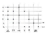
or similar materials are sandwiched between the horizontal and vertical wire layers. Each intersection or junction of the crossbar tile is configurable to be at a high-resistance state in which there is little or no current between the horizontal and vertical wires or at a low-resistance state in which current is permitted. Fig. 1 illustrates the configuration of a half-adder using a crossbar tile, as taught by Snider, with the nodes identifying junctions of the crossbar tile configured as low-resistance states. By setting different logic inputs A, NOT A, B, and NOT B to different row wires this configuration produces the sum and carry outputs typical for a half-adder. Connections between multiple half-adders may then be used to form full adders in accordance with conventional arithmetic architectures.
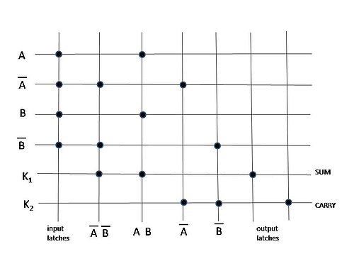
The second approach was described at the 2008 NSTI Nanotechnology Conference and combines crossbar latches with analog processing circuitry. This approach has the primary advantage of reducing the number of crossbar latch tiles necessary for arithmetic processing but may ultimately be limited in processing speed and precision due to the inclusion of analog circuit components. In order to perform computation this configuration takes advantage of the reconfigurability of crossbar latches and uses multiple programming iterations of the crossbar latches to perform binary arithmetic. For example, in Figs. 2A–2C each vertical wire of the column array represents a different binary bit significance value (1, 2, 4, 8, etc.) and binary numerical values are stored in each row using high resistance states to represent logic 0 and low resistance states to represent logic 1. Fig. 2A demonstrates performing the addition 1+2+3+4 by initially configuring the crossbar rows with corresponding binary resistance states 0001, 0010, 0011, and 0100.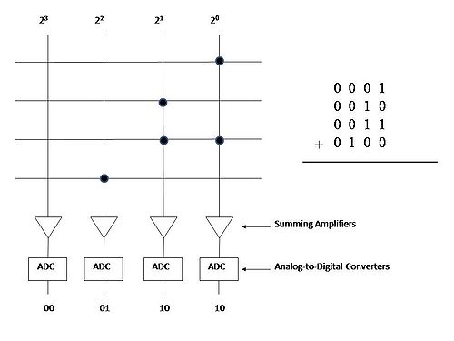 Summing amplifiers and analog to digital converters are used to sum the low-resistance states in each column, producing the analog outputs 0, 1, 2, 2. These analog values are converted to their binary equivalents 00, 01, 10, 10, which are then used to reconfigure the crossbar array for a second iteration as illustrated in Fig. 2B.
In the second iteration the placement of the reconfiguration bits are in accordance with the bit significance of the output column in the first iteration and the binary outputs in this case are 00,10,01,00. In the third iteration, since at most one bit per column is in the low-conductance state the output the A/D converters produce only two possible states which correspond to the expected result (1+2+3+4=10=1010(base-2)).
 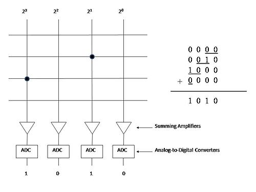 In a related patent application this process is described to be scaled up to 127-bit arithmetic processes including multiplication and division.
computing systems. One implementation of this is in the form of a neural network
formed from nanowires as discussed in a patent by Greg Snider of Hewlett-Packard. At the third international conference on Nano-Networks another implementation was proposed using analog circuitry and a memristor
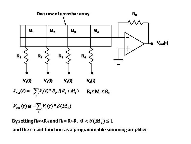
based crossbar configuration. As illustrated below the intersected wires of crossbar latches are formed to sandwich memristor material so as to generate variable resistance elements (M1-M4) tunable between a low resistance state (RL) and high resistance state (RH) and are connected to an operational amplifier
circuit which functions to sum input voltage signals V1(t)-V4(t) based on the state of the memristance materials at the intersections of the crossbar wires. One of the key advantages of such systems is that they integrate both memory and processing functions in a single circuit and thus avoid the delays inherent to conventional processor designs which separate the memory from the processor. This could prove useful to future designs of electronics for pattern recognition systems.
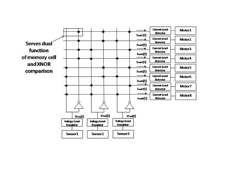
The circuit design used the crossbar latch structures to store resistance data patterns which were compared to sensed voltage patterns input to the crossbar columns. Each crossbar latch performed dual functions of memory storage and an XNOR comparison function to produce an analog row output current having a magnitude related to the similarity between the stored resistance pattern and the sensed voltage patterns. Depending on the binary voltage states of the sensors a different row produces current to drive a particular motor. The advantage of this design was explained to overcome the bottleneck of the Von Neumann architecture
by integrating memory storage and data processing in a common circuit.
Hewlett-Packard
Hewlett-Packard Company or HP is an American multinational information technology corporation headquartered in Palo Alto, California, USA that provides products, technologies, softwares, solutions and services to consumers, small- and medium-sized businesses and large enterprises, including...
in October 2001, that potentially could replace transistor
Transistor
A transistor is a semiconductor device used to amplify and switch electronic signals and power. It is composed of a semiconductor material with at least three terminals for connection to an external circuit. A voltage or current applied to one pair of the transistor's terminals changes the current...
s in some applications. Transistors are essential components of logic gates and memory cells in digital electronic systems. The historical trend for computer systems to become smaller and more powerful
Moore's Law
Moore's law describes a long-term trend in the history of computing hardware: the number of transistors that can be placed inexpensively on an integrated circuit doubles approximately every two years....
over the years is mostly due to techniques for producing ever smaller transistors. The memristor
Memristor
Memristor is a passive two-terminal electrical component envisioned by Leon Chua as a fundamental non-linear circuit element relating charge and magnetic flux linkage...
devices that make up a cross bar latch potentially can be made far smaller than any transistor.
The crossbar
Crossbar
- Structural engineering :* A primitive latch consisting of a post barring a door* The top tube of a bicycle frame* The horizontal member of many sports goals including those for hockey, association football, rugby league, rugby union and American football...
was introduced by Hewlett-Packard scientists in the Journal of Applied Physics, and allows much the same functionality of transistors, except on a molecular scale. It has been seen by many as an advancement as far above the transistor
Transistor
A transistor is a semiconductor device used to amplify and switch electronic signals and power. It is composed of a semiconductor material with at least three terminals for connection to an external circuit. A voltage or current applied to one pair of the transistor's terminals changes the current...
as the latter was to the vacuum tube. The crossbar latch
Latch
Latch may refer to:* Latch , a type of door or window fastener* Latch , a circuit used to store information** A latching relay* Latch , lock on a system data-structure like an index...
consists of a signal line crossed by two control lines. Depending on the voltages sent down the various lines, it can simulate the action of the three major logic gate
Logic gate
A logic gate is an idealized or physical device implementing a Boolean function, that is, it performs a logical operation on one or more logic inputs and produces a single logic output. Depending on the context, the term may refer to an ideal logic gate, one that has for instance zero rise time and...
s: AND
AND gate
The AND gate is a basic digital logic gate that implements logical conjunction - it behaves according to the truth table to the right. A HIGH output results only if both the inputs to the AND gate are HIGH . If neither or only one input to the AND gate is HIGH, a LOW output results...
, OR
OR gate
The OR gate is a digital logic gate that implements logical disjunction - it behaves according to the truth table to the right. A HIGH output results if one or both the inputs to the gate are HIGH . If neither input is HIGH, a LOW output results...
and NOT.
The abstract of the patent is as follows:
Applications in arithmetic processing
The first approach was developed by Greg Snider of Hewlett-Packard
Hewlett-Packard
Hewlett-Packard Company or HP is an American multinational information technology corporation headquartered in Palo Alto, California, USA that provides products, technologies, softwares, solutions and services to consumers, small- and medium-sized businesses and large enterprises, including...
and employs crossbar latches to replicate the functions of a half adder
Adder (electronics)
In electronics, an adder or summer is a digital circuit that performs addition of numbers.In many computers and other kinds of processors, adders are used not only in the arithmetic logic unit, but also in other parts of the processor, where they are used to calculate addresses, table indices, and...
, which form the basis of modern computational architectures. In this approach a crossbar tile is formed of a layer of horizontal row wires and a layer of vertical column wires in which memristor
Memristor
Memristor is a passive two-terminal electrical component envisioned by Leon Chua as a fundamental non-linear circuit element relating charge and magnetic flux linkage...
or similar materials are sandwiched between the horizontal and vertical wire layers. Each intersection or junction of the crossbar tile is configurable to be at a high-resistance state in which there is little or no current between the horizontal and vertical wires or at a low-resistance state in which current is permitted. Fig. 1 illustrates the configuration of a half-adder using a crossbar tile, as taught by Snider, with the nodes identifying junctions of the crossbar tile configured as low-resistance states. By setting different logic inputs A, NOT A, B, and NOT B to different row wires this configuration produces the sum and carry outputs typical for a half-adder. Connections between multiple half-adders may then be used to form full adders in accordance with conventional arithmetic architectures.
The second approach was described at the 2008 NSTI Nanotechnology Conference and combines crossbar latches with analog processing circuitry. This approach has the primary advantage of reducing the number of crossbar latch tiles necessary for arithmetic processing but may ultimately be limited in processing speed and precision due to the inclusion of analog circuit components. In order to perform computation this configuration takes advantage of the reconfigurability of crossbar latches and uses multiple programming iterations of the crossbar latches to perform binary arithmetic. For example, in Figs. 2A–2C each vertical wire of the column array represents a different binary bit significance value (1, 2, 4, 8, etc.) and binary numerical values are stored in each row using high resistance states to represent logic 0 and low resistance states to represent logic 1. Fig. 2A demonstrates performing the addition 1+2+3+4 by initially configuring the crossbar rows with corresponding binary resistance states 0001, 0010, 0011, and 0100.
In the second iteration the placement of the reconfiguration bits are in accordance with the bit significance of the output column in the first iteration and the binary outputs in this case are 00,10,01,00.
Applications of crossbar latch in neuromorphics
Crossbar latches have been suggested as components of neuromorphicNeuromorphic
Neuromorphic engineering or neuromorphic computing is a concept developed by Carver Mead, in the late 1980s, describing the use of very-large-scale integration systems containing electronic analog circuits to mimic neuro-biological architectures present in the nervous system...
computing systems. One implementation of this is in the form of a neural network
Neural network
The term neural network was traditionally used to refer to a network or circuit of biological neurons. The modern usage of the term often refers to artificial neural networks, which are composed of artificial neurons or nodes...
formed from nanowires as discussed in a patent by Greg Snider of Hewlett-Packard. At the third international conference on Nano-Networks another implementation was proposed using analog circuitry and a memristor
Memristor
Memristor is a passive two-terminal electrical component envisioned by Leon Chua as a fundamental non-linear circuit element relating charge and magnetic flux linkage...
based crossbar configuration. As illustrated below the intersected wires of crossbar latches are formed to sandwich memristor material so as to generate variable resistance elements (M1-M4) tunable between a low resistance state (RL) and high resistance state (RH) and are connected to an operational amplifier
Operational amplifier
An operational amplifier is a DC-coupled high-gain electronic voltage amplifier with a differential input and, usually, a single-ended output...
circuit which functions to sum input voltage signals V1(t)-V4(t) based on the state of the memristance materials at the intersections of the crossbar wires. One of the key advantages of such systems is that they integrate both memory and processing functions in a single circuit and thus avoid the delays inherent to conventional processor designs which separate the memory from the processor. This could prove useful to future designs of electronics for pattern recognition systems.
Applications of crossbar latch array in pattern recognition
At the 2nd International Multi-Conference on Engineering and Technological Innovation a crossbar latch circuit architecture was described for pattern recognition based on memristors.The circuit design used the crossbar latch structures to store resistance data patterns which were compared to sensed voltage patterns input to the crossbar columns. Each crossbar latch performed dual functions of memory storage and an XNOR comparison function to produce an analog row output current having a magnitude related to the similarity between the stored resistance pattern and the sensed voltage patterns. Depending on the binary voltage states of the sensors a different row produces current to drive a particular motor. The advantage of this design was explained to overcome the bottleneck of the Von Neumann architecture
Von Neumann architecture
The term Von Neumann architecture, aka the Von Neumann model, derives from a computer architecture proposal by the mathematician and early computer scientist John von Neumann and others, dated June 30, 1945, entitled First Draft of a Report on the EDVAC...
by integrating memory storage and data processing in a common circuit.
External links
- Research could send transistors the way of the vacuum tube (HP Press Release)
- HP claims molecular computing breakthrough (ComputerWorld)
- HP's 'Crossbar Latch' to Replace Transistors? (InterNetNews)