
Surface photovoltage
Encyclopedia
Surface photovoltage measurements are a widely used method to determine the minority carrier diffusion length of semiconductors. Since the transport of minority carriers determines the behavior of the p-n junction
s that are ubiquitous in semiconductor devices, surface photovoltage data can be very helpful in understanding their performance. As a contactless method, SPV is a popular technique for characterizing poorly understood compound semiconductors where the fabrication of ohmic contact
s or special device structures may be difficult.
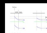
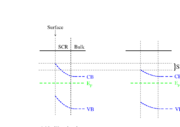 As the name suggests, SPV measurements involve monitoring the potential of a semiconductor surface while generating electron-hole pairs with a light source. The surfaces of semiconductors are often depletion region
s (or space charge
regions) where a built-in electric field due to defects has swept out mobile charge carriers. A reduced carrier density means that the Fermi level
is bent away from the electronic energy band
in which the majority carriers reside. This band-bending gives rise to a surface potential. When a light source creates electron-hole pairs deep within the semiconductor, they must diffuse through the bulk before reaching the surface depletion region. The photogenerated minority carriers have a shorter diffusion length than the much more numerous majority carriers, with which they can radiatively recombine. The change in surface potential upon illumination is therefore a measure of the ability of minority carriers to reach the surface, namely the minority carrier diffusion length. As always in diffusive processes, the diffusion length is approximately related to the lifetime
  by the expression
  , where
  is the diffusion coefficient
. The diffusion length is independent of any built-in fields in contrast to the drift
behavior of the carriers.
Note that the photogenerated majority carriers will also diffuse towards the surface but their number as a fraction of the thermally generated majority carrier density in a moderately doped semiconductor will be too small to create a measurable photovoltage. Both carrier types will also diffuse towards the rear contact where their collection can confuse interpretation of the data when the diffusion lengths are larger than the film thickness. In a real semiconductor, the measured diffusion length includes the effect of surface recombination, which is best understood through its effect on carrier lifetime:
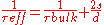
where is the effective carrier lifetime,
  is the bulk carrier lifetime,
  is the surface recombination velocity and
  is the film or wafer thickness. Even for well characterized materials, uncertainty about the value of the surface recombination velocity reduces the accuracy with which the diffusion length can be determined for thinner films.
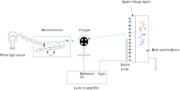 Surface photovoltage measurements are performed by placing a wafer
or sheet film of a semiconducting material on a ground electrode and positioning a kelvin probe
a small distance above the sample. The surface is illuminated with light whose wavelength
is scanned using a monochromator
so as to vary the absorption depth of the photons. The deeper in the semiconductor that carrier generation
occurs, the fewer the number of minority carriers that will reach the surface and the smaller the photovoltage. On a semiconductor whose spectral absorption coefficient is known, the minority carrier diffusion length can in principle be extracted from a measurement of photovoltage versus wavelength. The optical properties of a novel semiconductor may not be well known or may not be homogeneous across the sample. The temperature of the semiconductor must be carefully controlled during an SPV measurement test thermal drift complicate the comparison of different samples. Typically SPV measurements are done in an AC-coupled fashion using a chopped light source rather than a vibrating Kelvin probe.
detectors and bipolar transistors. In both cases the ratio of the diffusion length to the device dimensions determines the gain
. In photovoltaic devices, photodiode
s and field-effect transistor
s, the drift behavior due to built-in fields is more important under typical conditions than the diffusive behavior. Even so the SPV is a convenient method of measuring the density of impurity-derived recombination centers that limit device performance. SPV is performed both as an automated and routine test of material quality in a production environment and as an experimental tool to probe the behavior of less well studied semiconducting materials. Time-resolved photoluminescence
is an alternate contactless method of determining minority carrier transport properties.
P-n junction
A p–n junction is formed at the boundary between a P-type and N-type semiconductor created in a single crystal of semiconductor by doping, for example by ion implantation, diffusion of dopants, or by epitaxy .If two separate pieces of material were used, this would...
s that are ubiquitous in semiconductor devices, surface photovoltage data can be very helpful in understanding their performance. As a contactless method, SPV is a popular technique for characterizing poorly understood compound semiconductors where the fabrication of ohmic contact
Ohmic contact
An ohmic contact is a region on a semiconductor device that has been prepared so that the current-voltage curve of the device is linear and symmetric. If the I-V characteristic is non-linear and asymmetric, the contact is not ohmic, but is a blocking or Schottky contact...
s or special device structures may be difficult.
Theory
Depletion region
In semiconductor physics, the depletion region, also called depletion layer, depletion zone, junction region or the space charge region, is an insulating region within a conductive, doped semiconductor material where the mobile charge carriers have diffused away, or have been forced away by an...
s (or space charge
Space charge
Space charge is a concept in which excess electric charge is treated as a continuum of charge distributed over a region of space rather than distinct point-like charges...
regions) where a built-in electric field due to defects has swept out mobile charge carriers. A reduced carrier density means that the Fermi level
Fermi level
The Fermi level is a hypothetical level of potential energy for an electron inside a crystalline solid. Occupying such a level would give an electron a potential energy \epsilon equal to its chemical potential \mu as they both appear in the Fermi-Dirac distribution function,which...
is bent away from the electronic energy band
Electronic band structure
In solid-state physics, the electronic band structure of a solid describes those ranges of energy an electron is "forbidden" or "allowed" to have. Band structure derives from the diffraction of the quantum mechanical electron waves in a periodic crystal lattice with a specific crystal system and...
in which the majority carriers reside. This band-bending gives rise to a surface potential. When a light source creates electron-hole pairs deep within the semiconductor, they must diffuse through the bulk before reaching the surface depletion region. The photogenerated minority carriers have a shorter diffusion length than the much more numerous majority carriers, with which they can radiatively recombine. The change in surface potential upon illumination is therefore a measure of the ability of minority carriers to reach the surface, namely the minority carrier diffusion length. As always in diffusive processes, the diffusion length
is approximately related to the lifetime by the expression , where is the diffusion coefficientFick's law of diffusion
Fick's laws of diffusion describe diffusion and can be used to solve for the diffusion coefficient, D. They were derived by Adolf Fick in the year 1855.- Fick's first law :...
. The diffusion length is independent of any built-in fields in contrast to the drift
Drift velocity
The drift velocity is the average velocity that a particle, such as an electron, attains due to an electric field. It can also be referred to as Axial Drift Velocity since particles defined are assumed to be moving along a plane. In general, an electron will 'rattle around' in a conductor at the...
behavior of the carriers.
Note that the photogenerated majority carriers will also diffuse towards the surface but their number as a fraction of the thermally generated majority carrier density in a moderately doped semiconductor will be too small to create a measurable photovoltage. Both carrier types will also diffuse towards the rear contact where their collection can confuse interpretation of the data when the diffusion lengths are larger than the film thickness. In a real semiconductor, the measured diffusion length
includes the effect of surface recombination, which is best understood through its effect on carrier lifetime:where
is the effective carrier lifetime, is the bulk carrier lifetime, is the surface recombination velocity and is the film or wafer thickness. Even for well characterized materials, uncertainty about the value of the surface recombination velocity reduces the accuracy with which the diffusion length can be determined for thinner films.Experimental methods
Wafer (electronics)
A wafer is a thin slice of semiconductor material, such as a silicon crystal, used in the fabrication of integrated circuits and other microdevices...
or sheet film of a semiconducting material on a ground electrode and positioning a kelvin probe
Kelvin probe force microscope
Kelvin probe force microscopy , also known as surface potential microscopy, is a noncontact variant of atomic force microscopy that was invented in 1991. With KPFM, the work function of surfaces can be observed at atomic or molecular scales...
a small distance above the sample. The surface is illuminated with light whose wavelength
Wavelength
In physics, the wavelength of a sinusoidal wave is the spatial period of the wave—the distance over which the wave's shape repeats.It is usually determined by considering the distance between consecutive corresponding points of the same phase, such as crests, troughs, or zero crossings, and is a...
is scanned using a monochromator
Monochromator
A monochromator is an optical device that transmits a mechanically selectable narrow band of wavelengths of light or other radiation chosen from a wider range of wavelengths available at the input...
so as to vary the absorption depth of the photons. The deeper in the semiconductor that carrier generation
Carrier generation and recombination
In the solid state physics of semiconductors, carrier generation and recombination are processes by which mobile charge carriers are created and eliminated. Carrier generation and recombination processes are fundamental to the operation of many optoelectronic semiconductor devices, such as...
occurs, the fewer the number of minority carriers that will reach the surface and the smaller the photovoltage. On a semiconductor whose spectral absorption coefficient is known, the minority carrier diffusion length can in principle be extracted from a measurement of photovoltage versus wavelength. The optical properties of a novel semiconductor may not be well known or may not be homogeneous across the sample. The temperature of the semiconductor must be carefully controlled during an SPV measurement test thermal drift complicate the comparison of different samples. Typically SPV measurements are done in an AC-coupled fashion using a chopped light source rather than a vibrating Kelvin probe.
Significance
The minority carrier diffusion length is critical in determining the performance of devices such as photoconductingPhotoconductivity
Photoconductivity is an optical and electrical phenomenon in which a material becomes more electrically conductive due to the absorption of electromagnetic radiation such as visible light, ultraviolet light, infrared light, or gamma radiation....
detectors and bipolar transistors. In both cases the ratio of the diffusion length to the device dimensions determines the gain
Gain
In electronics, gain is a measure of the ability of a circuit to increase the power or amplitude of a signal from the input to the output. It is usually defined as the mean ratio of the signal output of a system to the signal input of the same system. It may also be defined on a logarithmic scale,...
. In photovoltaic devices, photodiode
Photodiode
A photodiode is a type of photodetector capable of converting light into either current or voltage, depending upon the mode of operation.The common, traditional solar cell used to generateelectric solar power is a large area photodiode....
s and field-effect transistor
Field-effect transistor
The field-effect transistor is a transistor that relies on an electric field to control the shape and hence the conductivity of a channel of one type of charge carrier in a semiconductor material. FETs are sometimes called unipolar transistors to contrast their single-carrier-type operation with...
s, the drift behavior due to built-in fields is more important under typical conditions than the diffusive behavior. Even so the SPV is a convenient method of measuring the density of impurity-derived recombination centers that limit device performance. SPV is performed both as an automated and routine test of material quality in a production environment and as an experimental tool to probe the behavior of less well studied semiconducting materials. Time-resolved photoluminescence
Photoluminescence
Photoluminescence is a process in which a substance absorbs photons and then re-radiates photons. Quantum mechanically, this can be described as an excitation to a higher energy state and then a return to a lower energy state accompanied by the emission of a photon...
is an alternate contactless method of determining minority carrier transport properties.
External links
- The Minority Carrier Lifetime in silicon wafer
- Semilab vendor of commercial SPV and Minority Carrier Lifetime measurement systems
- Semiconductor Diagnostics vendor of commercial SPV systems
- KP Technology vendors of and consultants about Kelvin probes
- McAllister Kelvin probe manufacturers
- ASTM standard F391-96 "Standard Test Methods for Minority Carrier Diffusion Length in Extrinsic Semiconductors by Measurement of Steady-State Surface Photovoltage"