

Successive approximation ADC
Encyclopedia
A successive approximation ADC is a type of analog-to-digital converter
that converts a continuous analog
waveform into a discrete digital
representation via a binary search through all possible quantization
levels before finally converging upon a digital output for each conversion.
 Key
Key
The successive approximation register is initialized so that the most significant bit
(MSB) is equal to a digital
1. This code is fed into the DAC, which then supplies the analog equivalent of this digital code (Vref/2) into the comparator circuit for comparison with the sampled input voltage. If this analog voltage exceeds Vin the comparator causes the SAR to reset this bit; otherwise, the bit is left a 1. Then the next bit is set to 1 and the same test is done, continuing this binary search
until every bit in the SAR has been tested. The resulting code is the digital approximation of the sampled input voltage and is finally output by the DAC at the end of the conversion (EOC).
Mathematically, let Vin = xVref, so x in [-1, 1] is the normalized input voltage. The objective is to approximately digitize x to an accuracy of 1/2n. The algorithm proceeds as follows:
where, s(x) is the signum-function(sgn(x)) (+1 for x ≥ 0, -1 for x < 0). It follows using mathematical induction that |xn - x| ≤ 1/2n.
As shown in the above algorithm, a SAR ADC requires:
 One of the most common implementations of the successive approximation ADC, the charge-redistribution successive approximation ADC, uses a charge scaling DAC
. The charge scaling DAC simply consists of an array of individually switched binary-weighted capacitors. The amount of charge upon each capacitor in the array is used to perform the aforementioned binary search in conjunction with a comparator internal to the DAC and the successive approximation register.
The DAC conversion is performed in four basic steps:
Analog-to-digital converter
An analog-to-digital converter is a device that converts a continuous quantity to a discrete time digital representation. An ADC may also provide an isolated measurement...
that converts a continuous analog
Analog signal
An analog or analogue signal is any continuous signal for which the time varying feature of the signal is a representation of some other time varying quantity, i.e., analogous to another time varying signal. It differs from a digital signal in terms of small fluctuations in the signal which are...
waveform into a discrete digital
Digital
A digital system is a data technology that uses discrete values. By contrast, non-digital systems use a continuous range of values to represent information...
representation via a binary search through all possible quantization
Quantization (signal processing)
Quantization, in mathematics and digital signal processing, is the process of mapping a large set of input values to a smaller set – such as rounding values to some unit of precision. A device or algorithmic function that performs quantization is called a quantizer. The error introduced by...
levels before finally converging upon a digital output for each conversion.
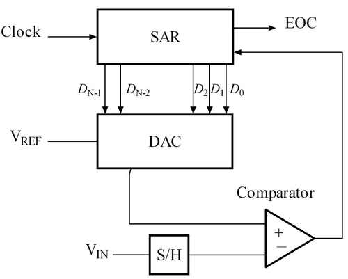
Block diagram
- DAC = Digital-to-Analog converter
- EOC = end of conversion
- SAR = successive approximation register
- S/H = sample and hold circuit
- Vin = input voltage
- Vref = reference voltage
Algorithm
The successive approximation Analog to digital converter circuit typically consists of four chief subcircuits:-
- A sample and hold circuit to acquire the input voltageVoltageVoltage, otherwise known as electrical potential difference or electric tension is the difference in electric potential between two points — or the difference in electric potential energy per unit charge between two points...
(Vin). - An analog voltage comparator that compares Vin to the output of the internal DACDigital-to-analog converterIn electronics, a digital-to-analog converter is a device that converts a digital code to an analog signal . An analog-to-digital converter performs the reverse operation...
and outputs the result of the comparison to the successive approximation registerProcessor registerIn computer architecture, a processor register is a small amount of storage available as part of a CPU or other digital processor. Such registers are addressed by mechanisms other than main memory and can be accessed more quickly...
(SAR). - A successive approximation register subcircuit designed to supply an approximate digital code of Vin to the internal DAC.
- An internal reference DAC that supplies the comparatorComparatorIn electronics, a comparator is a device that compares two voltages or currents and switches its output to indicate which is larger. They are commonly used in devices such as Analog-to-digital converters .- Input voltage range :...
with an analog voltage equivalent of the digital code output of the SAR for comparison with Vin.
- A sample and hold circuit to acquire the input voltage
The successive approximation register is initialized so that the most significant bit
Most significant bit
In computing, the most significant bit is the bit position in a binary number having the greatest value...
(MSB) is equal to a digital
Digital
A digital system is a data technology that uses discrete values. By contrast, non-digital systems use a continuous range of values to represent information...
1. This code is fed into the DAC, which then supplies the analog equivalent of this digital code (Vref/2) into the comparator circuit for comparison with the sampled input voltage. If this analog voltage exceeds Vin the comparator causes the SAR to reset this bit; otherwise, the bit is left a 1. Then the next bit is set to 1 and the same test is done, continuing this binary search
Binary search algorithm
In computer science, a binary search or half-interval search algorithm finds the position of a specified value within a sorted array. At each stage, the algorithm compares the input key value with the key value of the middle element of the array. If the keys match, then a matching element has been...
until every bit in the SAR has been tested. The resulting code is the digital approximation of the sampled input voltage and is finally output by the DAC at the end of the conversion (EOC).
Mathematically, let Vin = xVref, so x in [-1, 1] is the normalized input voltage. The objective is to approximately digitize x to an accuracy of 1/2n. The algorithm proceeds as follows:
-
- Initial approximation x0 = 0.
- ith approximation xi = xi-1 - s(xi-1 - x)/2i.
where, s(x) is the signum-function(sgn(x)) (+1 for x ≥ 0, -1 for x < 0). It follows using mathematical induction that |xn - x| ≤ 1/2n.
As shown in the above algorithm, a SAR ADC requires:
-
- An input voltage source Vin.
- A reference voltage source Vref to normalize the input.
- A DAC to convert the ith approximation xi to a voltage.
- A Comparator to perform the function s(xi - x) by comparing the DAC's voltage with the input voltage.
- A Register to store the output of the comparator and apply xi-1 - s(xi-1 - x)/2i.
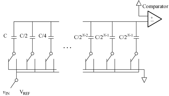
Charge-redistribution successive approximation ADC
Digital-to-analog converter
In electronics, a digital-to-analog converter is a device that converts a digital code to an analog signal . An analog-to-digital converter performs the reverse operation...
. The charge scaling DAC simply consists of an array of individually switched binary-weighted capacitors. The amount of charge upon each capacitor in the array is used to perform the aforementioned binary search in conjunction with a comparator internal to the DAC and the successive approximation register.
The DAC conversion is performed in four basic steps:
-
- First, the capacitor array is completely discharged to the offset voltage of the comparator, VOS. This step provides automatic offset cancellation(i.e. The offset voltage represents nothing but dead charge which can't be juggled by the capacitors).
- Next, all of the capacitors within the array are switched to the input signal, vIN. The capacitors now have a charge equal to their respective capacitance times the input voltage minus the offset voltage upon each of them.
- In the third step, the capacitors are then switched so that this charge is applied across the comparator's input, creating a comparator input voltage equal to -vIN.
- Finally, the actual conversion process proceeds. First, the MSB capacitor is switched to VREF, which corresponds to the full-scale range of the ADC. Due to the binary-weighting of the array the MSB capacitor forms a 1:1 divided between it and the rest of the array. Thus, the input voltage to the comparator is now -vIN plus VREF/2. Subsequently, if vIN is greater than VREF/2 then the comparator outputs a digital 1 as the MSB, otherwise it outputs a digital 0 as the MSB. Each capacitor is tested in the same manner until the comparator input voltage converges to the offset voltage, or at least as close as possible given the resolution of the DAC.