
.gif)
Physical design (electronics)
Encyclopedia
In integrated circuit design
, physical design is a step in the standard design cycle which follows after the circuit design
. At this step, circuit representations of the components (devices and interconnects) of the design are converted into geometric representations of shapes which, when manufactured in the corresponding layers of materials, will ensure the required functioning of the components. This geometric representation is called integrated circuit layout
. This step is usually split into several sub-steps, which include both design and verification and validation of the layout.
Modern day Integrated Circuit
(IC) design is split up into Front-end design using HDL's, Verification and Back-end Design or Physical Design. The next step after Physical Design is the Manufacturing process or Fabrication Process that is done in the Wafer Fabrication Houses. Fab-houses fabricate designs onto silicon dies which are then packaged into ICs.
Each of the phases mentioned above have Design Flows associated with them. These Design Flows lay down the process and guide-lines/framework for that phase. Physical Design flow uses the technology libraries that are provided by the fabrication houses. These technology files provide information regarding the type of Silicon wafer used, the standard-cells used, the layout rules, etc.
Technologies are commonly classified according to minimal feature size. Standard sizes, in the order of miniaturization, are 2μm
, 1μm , 0.5μm , 0.35μm, 0.25μm, 180nm
, 130nm, 90nm, 65nm, 45nm, 28nm, 22nm, 18nm...
They may be also classified according to major manufacturing approaches: n-Well process, twin-well process, SOI
process, etc.
The main steps in the flow are:
These steps are just the basic. There are detailed PD Flows that are used depending on the Tools used and the methodology/technology. Some of the tools/software used in the back-end design are :
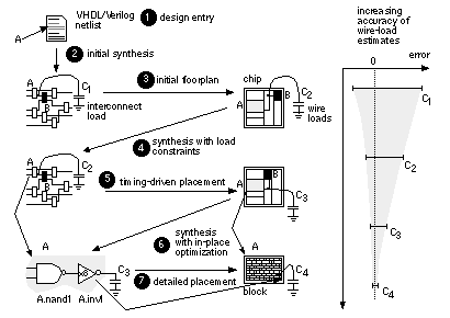
A more detailed Physical Design Flow is shown below. Here you can see the exact steps and the tools used in each step outlined.
During the synthesis process, constraints are applied to ensure that the design meets the required functionality and speed (specifications). Only after the netlist is verified for functionality and timing is it sent for the Physical Design flow.
Based on the area of the design and the hierarchy, a suitable floorplan is decided upon. Floor Planning takes into account the macro's used in the design, memory, other IP cores and their placement needs, the routing possibilities and also the area of the entire design. Floor planning also decides the IO structure, aspect ratio of the design. A bad floor-plan will lead to waste-age of die area and routing congestion.
In many design methodologies, Area and Speed are considered to be things that should be traded off against each other. The reason this is so is probably because there are limited routing resources, and the more routing resources that are used, the slower the design will operate. Optimizing for minimum area allows the design to use fewer resources, but also allows the sections of the design to be closer together. This leads to shorter interconnect distances, less routing resources to be used, faster end-to-end signal paths, and even faster and more consistent place and route times. Done correctly , there are no negatives to Floor-planning.
As a general rule, data-path sections benefit most from Floorplanning, and random logic, state machines, and other non-structured logic can safely be left to the placer section of the place and route software.
Data paths are typically the areas of your design where multiple bits are processed in parallel with each bit being modified the same way with maybe some influence from adjacent bits. Example structures that make up data paths are Adders, Subtractors, Counters, Registers, and Muxes.
Placement is performed in four optimization phases:
Rigidity is the term coined in Astro to indicate the relaxation of constraints. Higher the rigidity tighter is the constraints.
In clock tree optimization (CTO) clock can be shielded so that noise is not coupled to other signals. But shielding increases area by 12 to 15%. Since the clock signal is global in nature the same metal layer used for power routing is used for clock also. CTO is achieved by buffer sizing, gate sizing, buffer relocation, level adjustment and HFN synthesis. We try to improve setup slack in pre-placement, in placement and post placement optimization before CTS stages while neglecting hold slack. In post placement optimization after CTS hold slack is improved. As a result of CTS lot of buffers are added. Generally for 100k gates around 650 buffers are added.
stream format that is sent to a semiconductor fabrication plant (fab).
Integrated circuit design
Integrated circuit design, or IC design, is a subset of electrical engineering and computer engineering, encompassing the particular logic and circuit design techniques required to design integrated circuits, or ICs...
, physical design is a step in the standard design cycle which follows after the circuit design
Circuit design
The process of circuit design can cover systems ranging from complex electronic systems all the way down to the individual transistors within an integrated circuit...
. At this step, circuit representations of the components (devices and interconnects) of the design are converted into geometric representations of shapes which, when manufactured in the corresponding layers of materials, will ensure the required functioning of the components. This geometric representation is called integrated circuit layout
Integrated circuit layout
Integrated circuit layout, also known IC layout, IC mask layout, or mask design, is the representation of an integrated circuit in terms of planar geometric shapes which correspond to the patterns of metal, oxide, or semiconductor layers that make up the components of the integrated circuit.When...
. This step is usually split into several sub-steps, which include both design and verification and validation of the layout.
Modern day Integrated Circuit
Integrated circuit
An integrated circuit or monolithic integrated circuit is an electronic circuit manufactured by the patterned diffusion of trace elements into the surface of a thin substrate of semiconductor material...
(IC) design is split up into Front-end design using HDL's, Verification and Back-end Design or Physical Design. The next step after Physical Design is the Manufacturing process or Fabrication Process that is done in the Wafer Fabrication Houses. Fab-houses fabricate designs onto silicon dies which are then packaged into ICs.
Each of the phases mentioned above have Design Flows associated with them. These Design Flows lay down the process and guide-lines/framework for that phase. Physical Design flow uses the technology libraries that are provided by the fabrication houses. These technology files provide information regarding the type of Silicon wafer used, the standard-cells used, the layout rules, etc.
Technologies are commonly classified according to minimal feature size. Standard sizes, in the order of miniaturization, are 2μm
Micrometre
A micrometer , is by definition 1×10⁻⁶ of a meter .In plain English, it means one-millionth of a meter . Its unit symbol in the International System of Units is μm...
, 1μm , 0.5μm , 0.35μm, 0.25μm, 180nm
Nanometre
A nanometre is a unit of length in the metric system, equal to one billionth of a metre. The name combines the SI prefix nano- with the parent unit name metre .The nanometre is often used to express dimensions on the atomic scale: the diameter...
, 130nm, 90nm, 65nm, 45nm, 28nm, 22nm, 18nm...
They may be also classified according to major manufacturing approaches: n-Well process, twin-well process, SOI
Silicon on insulator
Silicon on insulator technology refers to the use of a layered silicon-insulator-silicon substrate in place of conventional silicon substrates in semiconductor manufacturing, especially microelectronics, to reduce parasitic device capacitance and thereby improving performance...
process, etc.
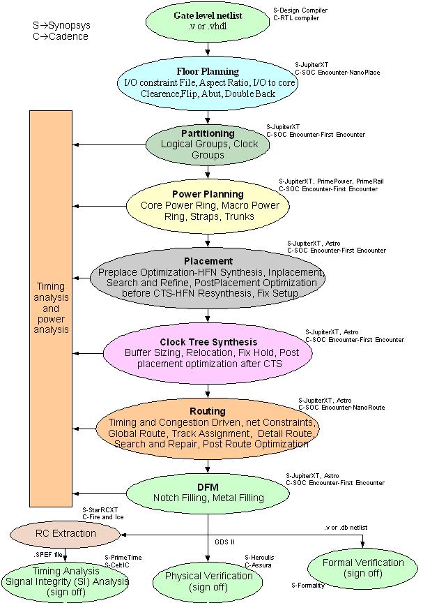
Physical Design Flow
A typical Back-end Flow is shown belowThe main steps in the flow are:
- Design Netlist (after synthesis)
- Floor Planning
- Partitioning
- Placement
- Clock-tree Synthesis (CTS)
- Routing
- Physical Verification
- GDS II Generation
These steps are just the basic. There are detailed PD Flows that are used depending on the Tools used and the methodology/technology. Some of the tools/software used in the back-end design are :
- Cadence (SOC Encounter, VoltageStorm, NanoRoute)
- Synopsys (Design Compiler)
- Magma (BlastFusion, etc)
- Mentor Graphics (Olympus SoC, IC-Station, Calibre)
A more detailed Physical Design Flow is shown below. Here you can see the exact steps and the tools used in each step outlined.
Design Netlist
A Netlist/Gate-level netlist is the end result of the Synthesis process. Synthesis converts the RTL design usually coded in VHDL or Verilog HDL to gate-level descriptions which the next set of tools can read/understand. This netlist contains information on the cells used, their interconnections, area used, and other details. Typical synthesis tools are:- Cadence RTL Compiler/Build Gates/Physically Knowledgeable Synthesis (PKS)
- Synopsys Design Compiler
During the synthesis process, constraints are applied to ensure that the design meets the required functionality and speed (specifications). Only after the netlist is verified for functionality and timing is it sent for the Physical Design flow.
Floor Planning
The first step in the Physical Design flow is Floor Planning. Floorplanning is the process of identifying structures that should be placed close together, and allocating space for them in such a manner as to meet the sometimes conflicting goals of available space (cost of the chip), required performance, and the desire to have everything close to everything else.Based on the area of the design and the hierarchy, a suitable floorplan is decided upon. Floor Planning takes into account the macro's used in the design, memory, other IP cores and their placement needs, the routing possibilities and also the area of the entire design. Floor planning also decides the IO structure, aspect ratio of the design. A bad floor-plan will lead to waste-age of die area and routing congestion.
In many design methodologies, Area and Speed are considered to be things that should be traded off against each other. The reason this is so is probably because there are limited routing resources, and the more routing resources that are used, the slower the design will operate. Optimizing for minimum area allows the design to use fewer resources, but also allows the sections of the design to be closer together. This leads to shorter interconnect distances, less routing resources to be used, faster end-to-end signal paths, and even faster and more consistent place and route times. Done correctly , there are no negatives to Floor-planning.
As a general rule, data-path sections benefit most from Floorplanning, and random logic, state machines, and other non-structured logic can safely be left to the placer section of the place and route software.
Data paths are typically the areas of your design where multiple bits are processed in parallel with each bit being modified the same way with maybe some influence from adjacent bits. Example structures that make up data paths are Adders, Subtractors, Counters, Registers, and Muxes.
Partitioning
Partitioning is a process of dividing the chip into small blocks. This is done mainly to separate different functional blocks and also to make placement and routing easier. Partitioning can be done in the RTL design phase when the design engineer partitions the entire design into sub-blocks and then proceeds to design each module. These modules are linked together in the main module called the TOP LEVEL module. This kind of partitioning is commonly referred to as Logical Partitioning.Placement
Before the start of placement optimization all Wire Load Models (WLM) are removed. Placement uses RC values from Virtual Route (VR) to calculate timing. VR is the shortest Manhattan distance between two pins. VR RCs are more accurate than WLM RCs.Placement is performed in four optimization phases:
- Pre-placement optimization
- In placement optimization
- Post Placement Optimization (PPO) before clock tree synthesis (CTS)
- PPO after CTS.
- Pre-placement Optimization optimizes the netlist before placement, HFNs are collapsed. It can also downsize the cells.
- In-placement optimization re-optimizes the logic based on VR. This can perform cell sizing, cell moving, cell bypassing, net splitting, gate duplication, buffer insertion, area recovery. Optimization performs iteration of setup fixing, incremental timing and congestion driven placement.
- Post placement optimization before CTS performs netlist optimization with ideal clocks. It can fix setup, hold, max trans/cap violations. It can do placement optimization based on global routing. It re does HFN synthesis.
- Post placement optimization after CTS optimizes timing with propagated clock. It tries to preserve clock skew.
Clock tree synthesis
The goal of clock tree synthesis (CTS) is to minimize skew and insertion delay. Clock is not propagated before CTS as shown in the picture. After CTS hold slack should improve. Clock tree begins at .sdc defined clock source and ends at stop pins of flop. There are two types of stop pins known as ignore pins and sync pins. ‘Don’t touch’ circuits and pins in front end (logic synthesis) are treated as ‘ignore’ circuits or pins at back end (physical synthesis). ‘Ignore’ pins are ignored for timing analysis. If clock is divided then separate skew analysis is necessary.- Global skew achieves zero skew between two synchronous pins without considering logic relationship.
- Local skew achieves zero skew between two synchronous pins while considering logic relationship.
- If clock is skewed intentionally to improve setup slack then it is known as useful skew.
Rigidity is the term coined in Astro to indicate the relaxation of constraints. Higher the rigidity tighter is the constraints.
In clock tree optimization (CTO) clock can be shielded so that noise is not coupled to other signals. But shielding increases area by 12 to 15%. Since the clock signal is global in nature the same metal layer used for power routing is used for clock also. CTO is achieved by buffer sizing, gate sizing, buffer relocation, level adjustment and HFN synthesis. We try to improve setup slack in pre-placement, in placement and post placement optimization before CTS stages while neglecting hold slack. In post placement optimization after CTS hold slack is improved. As a result of CTS lot of buffers are added. Generally for 100k gates around 650 buffers are added.
Routing
There are two types of routing in the physical design process, global routing and detailed routing. Global routing allocates routing resources that are used for connections. Detailed routing assigns routes to specific metal layers and routing tracks within the global routing resources.Physical Verification
Physical verification checks the correctness of the layout design. This includes verifying that the layout- Complies with all technology requirements – Design Rule Checking (DRC)
- Is consistent with the original netlist – Layout vs. Schematic (LVS)
- Has no antenna effects – Antenna Rule Checking
- Complies with all electrical requirements – Electrical Rule Checking (ERC).
GDSII Generation
Once the design has been physically verified, optical-lithography masks are generated for manufacturing. The layout is represented in the GDSIIGDSII
GDSII stream format, common acronym GDSII, is a database file format which is the de facto industry standard for data exchange of integrated circuit or IC layout artwork. It is a binary file format representing planar geometric shapes, text labels, and other information about the layout in...
stream format that is sent to a semiconductor fabrication plant (fab).