
High Resolution Transmission Electron Microscopy
Encyclopedia
High-resolution transmission electron microscopy (HRTEM) is an imaging mode of the transmission electron microscope (TEM) that allows the imaging of the crystallographic structure of a sample at an atomic scale. Because of its high resolution, it is an invaluable tool to study nanoscale properties of crystalline material such as semiconductors and metals. At present, the highest resolution realised is 0.8 ångström (0.08 nm) with microscopes such as the OAM at NCEM
. Ongoing research and development such as efforts in the framework of TEAM
will soon push the resolution of HRTEM to 0.5 Å. At these small scales, individual atoms and crystalline defects can be imaged. Since all crystal structures are 3-dimensional, it may be necessary to combine several views of the crystal, taken from different angles, into a 3D map. This technique is called electron crystallography
.
One of the difficulties with HRTEM is that image formation relies on phase-contrast. In phase-contrast imaging
, contrast is not necessarily intuitively interpretable as the image is influenced by strong aberrations of the imaging lenses in the microscope. One major aberration is caused by focus and astigmatism, which often can be estimated from the Fourier transform of the HRTEM image.
 ]
]
As opposed to conventional microscopy, HRTEM does not use amplitudes, i.e. absorption by the sample, for image formation. Instead, contrast arises from the interference in the image plane of the electron wave with itself. Due to our inability to record the phase of these waves, we generally measure the amplitude resulting from this interference, however the phase of the electron wave still carries the information about the sample and generates contrast in the image, thus the name phase-contrast imaging. This, however is true only if the sample is thin enough so that amplitude variations only slightly affect the image (the so-called weak phase object approximation, WPOA).
The interaction of the electron wave with the crystallographic structure of the sample is not entirely understood yet, but a qualitative idea of the interaction can readily be obtained. Each imaging electron interacts independently with the sample. Above the sample, the wave of an electron can be approximated as a plane wave incident on the sample surface. As it penetrates the sample, it is attracted by the positive atomic potentials of the atom cores, and channels along the atom columns of the crystallographic lattice (s-state model). At the same time, the interaction between the electron wave in different atom columns leads to Bragg diffraction. The exact description of dynamical scattering of electrons in a sample not satisfying the WPOA (almost all real samples) still remains the holy grail of electron microscopy. However, the physics of electron scattering and electron microscope image formation are sufficiently well known to allow accurate simulation of electron microscope images.
As a result of the interaction with the sample, the electron exit wave right below the sample φe(x,u) as a function of the spatial coordinate x is a superposition of a plane wave and a multitude of diffracted beams with different in plane spatial frequencies
u (high spatial frequencies correspond to large distances from the optical axis). The phase change of φe(x,u) compared to the incident wave peaks at the location of the atom columns. The exit wave now passes through the imaging system of the microscope where it undergoes further phase change and interferes as the image wave in the imaging plane (photo plate or CCD). It is important to realize, that the recorded image is NOT a direct representation of the samples crystallographic structure. For instance, high intensity might or might not indicate the presence of an atom column in that precise location (see simulation). The relationship between the exit wave and the image wave is a highly nonlinear one and is a function of the aberrations of the microscope. It is described by the contrast transfer function.
(CTF) is a function of limiting apertures and aberrations
in the imaging lenses of a microscope. It describes their effect on the phase of the exit wave φe(x,u) and propagates it to the image wave. Following Williams and Carter, if we assume the WPOA holds (thin sample) the CTF becomes
where A(u) is the aperture function, E(u) describes the attenuation of the wave for higher spatial frequency
u, also called envelope function. χ(u) is a function of the aberrations of the electron optical system.
The last, sinusoidal term of the CTF will determine the sign with which components of frequency u will enter contrast in the final image. If one takes into account only spherical aberration to third order and defocus, χ is rotationally symmetric about the optical axis of the microscope and thus only depends on the modulus u = |u|, given by
where Cs is the spherical aberration coefficient, λ is the electron wavelength, and Δf is the defocus. In TEM, defocus can easily be controlled and measured to high precision. Thus one can easily alter the shape of the CTF by defocusing the sample. Contrary to optical applications, defocusing can actually increase the precision and interpretability of the micrographs.
The aperture function cuts off beams scattered above a certain critical angle (given by the objective pole piece for ex), thus effectively limiting the attainable resolution. However it is the envelope function E(u) which usually dampens the signal of beams scattered at high angles, and imposes a maximum to the transmitted spatial frequency. This maximum determines the highest resolution attainable with a microscope and is known as the information limit. E(u) can be described as a product of single envelopes:
due to
Specimen drift and vibration can be minimized relatively easily by a suitable working environment. It is usually the spherical aberration Cs that limits spatial coherency and defines Es(u) and the chromatical aberration, together with current and voltage instabilities that define the temporal coherency in Ec(u). These two envelopes determine the information limit.
If we consider the probe to have a Gaussian distribution of electron intensity, the spatial envelope function is given by
where α is the semiangle describing the Gaussian distribution. Clearly, if the spherical aberration Cs were zero, this envelope function would be a constant one for Gaussian focus. Else, the damping due to this envelope function can be minimized by optimizing the defocus at which the image is recorded (Lichte defocus).
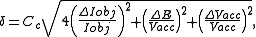
The temporal envelope function can be expressed as
here δ is the focus spread due to chromatical aberration Cc:
The terms and
and  represent instabilities in of the currents in the objective lens and the high voltage supply of the electron gun.
  is the energy spread of electrons leaving the gun.
The information limit of current (2006) microscopes lies little below 1 Å. The TEAM
project aims at pushing the information limit to 0.5 Å. To do so it will be fully corrected for third and fifth order spherical aberration as well as chromatical aberration. Further, the electron beam will be highly monochromatised and current and voltage have to be stabilized.
 Choosing the optimum defocus is crucial to fully exploit the capabilities of an electron microscope in HRTEM mode. However, there is no simple answer as to which one is the best.
In Gaussian focus one sets the defocus to zero, the sample is in focus. As a consequence contrast in the image plane gets its image components from the minimal area of the sample, the contrast is localized (no blurring and information overlap from other parts of the sample). The CTF now becomes a function that oscillates quickly with Csu4. What this means is that for certain diffracted beams with a given spatial frequency u the contribution to contrast in the recorded image will be reversed, thus making interpretation of the image difficult.
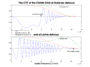
where the factor 1.2 defines the extended Scherzer defocus. For the CM300 at NCEM
, Cs = 0.6mm and an accelerating voltage of 300keV (λ = 1.97 pm) (Wavelength calculation) result in ΔfScherzer = -41.25 nm.
The point resolution of a microscope is defined as the spatial frequency ures where the CTF crosses the abscissa
for the first time. At Scherzer defocus this value is maximized:
which corresponds to 6.1 nm−1 on the CM300. Contributions with a spatial frequency higher than the point resolution can be filtered out with an appropriate aperture leading to easily interpretable images at the cost of a lot of information lost.

where umax is the maximum transmitted spatial frequency. For the CM300 with an information limit of 0.8 Å Lichte defocus lies at −272 nm.
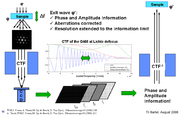 To calculate back to φe(x,u) the wave in the image plane is back propagated numerically to the sample. If all properties of the microscope are well known, it is possible to recover the real exit wave with very high accuracy.
First however, both phase and amplitude of the electron wave in the image plane must be measured. As our instruments only record amplitudes, an alternative method to recover the phase has to be used. There are two methods in use today:
Both methods extend the point resolution of the microscope the information limit, which is the highest possible resolution achievable on a given machine. The ideal defocus value for this type of imaging is known as Lichte defocus and is usually several hundred nanometers negative.
National Center for Electron Microscopy
The National Center for Electron Microscopy is a U.S. Department of Energy national user facility at Lawrence Berkeley National Laboratory in Berkeley, California, for unclassified scientific research using advanced electron microscopy. It is managed and owned by the University of California....
. Ongoing research and development such as efforts in the framework of TEAM
Transmission Electron Aberration-corrected Microscope
Transmission Electron Aberration-Corrected Microscope is a collaborative research project between four US laboratories and two companies. It is based at the Lawrence Berkeley National Laboratory in Berkeley, California and involves Argonne National Laboratory, Oak Ridge National Laboratory and...
will soon push the resolution of HRTEM to 0.5 Å. At these small scales, individual atoms and crystalline defects can be imaged. Since all crystal structures are 3-dimensional, it may be necessary to combine several views of the crystal, taken from different angles, into a 3D map. This technique is called electron crystallography
Electron crystallography
Electron crystallography is a method to determine the arrangement of atoms in solids using a transmission electron microscope .- Comparison with X-ray crystallography :...
.
One of the difficulties with HRTEM is that image formation relies on phase-contrast. In phase-contrast imaging
Phase-contrast imaging
Phase-contrast imaging is a method of imaging that has a range of different applications. It exploits differences in the refractive index of different materials to differentiate between structures under analysis...
, contrast is not necessarily intuitively interpretable as the image is influenced by strong aberrations of the imaging lenses in the microscope. One major aberration is caused by focus and astigmatism, which often can be estimated from the Fourier transform of the HRTEM image.
Image contrast and interpretation
As opposed to conventional microscopy, HRTEM does not use amplitudes, i.e. absorption by the sample, for image formation. Instead, contrast arises from the interference in the image plane of the electron wave with itself. Due to our inability to record the phase of these waves, we generally measure the amplitude resulting from this interference, however the phase of the electron wave still carries the information about the sample and generates contrast in the image, thus the name phase-contrast imaging. This, however is true only if the sample is thin enough so that amplitude variations only slightly affect the image (the so-called weak phase object approximation, WPOA).
The interaction of the electron wave with the crystallographic structure of the sample is not entirely understood yet, but a qualitative idea of the interaction can readily be obtained. Each imaging electron interacts independently with the sample. Above the sample, the wave of an electron can be approximated as a plane wave incident on the sample surface. As it penetrates the sample, it is attracted by the positive atomic potentials of the atom cores, and channels along the atom columns of the crystallographic lattice (s-state model). At the same time, the interaction between the electron wave in different atom columns leads to Bragg diffraction. The exact description of dynamical scattering of electrons in a sample not satisfying the WPOA (almost all real samples) still remains the holy grail of electron microscopy. However, the physics of electron scattering and electron microscope image formation are sufficiently well known to allow accurate simulation of electron microscope images.
As a result of the interaction with the sample, the electron exit wave right below the sample φe(x,u) as a function of the spatial coordinate x is a superposition of a plane wave and a multitude of diffracted beams with different in plane spatial frequencies
Spatial frequency
In mathematics, physics, and engineering, spatial frequency is a characteristic of any structure that is periodic across position in space. The spatial frequency is a measure of how often sinusoidal components of the structure repeat per unit of distance. The SI unit of spatial frequency is...
u (high spatial frequencies correspond to large distances from the optical axis). The phase change of φe(x,u) compared to the incident wave peaks at the location of the atom columns. The exit wave now passes through the imaging system of the microscope where it undergoes further phase change and interferes as the image wave in the imaging plane (photo plate or CCD). It is important to realize, that the recorded image is NOT a direct representation of the samples crystallographic structure. For instance, high intensity might or might not indicate the presence of an atom column in that precise location (see simulation). The relationship between the exit wave and the image wave is a highly nonlinear one and is a function of the aberrations of the microscope. It is described by the contrast transfer function.
The phase contrast transfer function
The phase contrast transfer functionOptical transfer function
The optical transfer function of an imaging system is the true measure of resolution that the system is capable of...
(CTF) is a function of limiting apertures and aberrations
Aberration in optical systems
Aberrations are departures of the performance of an optical system from the predictions of paraxial optics. Aberration leads to blurring of the image produced by an image-forming optical system. It occurs when light from one point of an object after transmission through the system does not converge...
in the imaging lenses of a microscope. It describes their effect on the phase of the exit wave φe(x,u) and propagates it to the image wave. Following Williams and Carter, if we assume the WPOA holds (thin sample) the CTF becomes

where A(u) is the aperture function, E(u) describes the attenuation of the wave for higher spatial frequency
Spatial frequency
In mathematics, physics, and engineering, spatial frequency is a characteristic of any structure that is periodic across position in space. The spatial frequency is a measure of how often sinusoidal components of the structure repeat per unit of distance. The SI unit of spatial frequency is...
u, also called envelope function. χ(u) is a function of the aberrations of the electron optical system.
The last, sinusoidal term of the CTF will determine the sign with which components of frequency u will enter contrast in the final image. If one takes into account only spherical aberration to third order and defocus, χ is rotationally symmetric about the optical axis of the microscope and thus only depends on the modulus u = |u|, given by
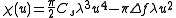
where Cs is the spherical aberration coefficient, λ is the electron wavelength, and Δf is the defocus. In TEM, defocus can easily be controlled and measured to high precision. Thus one can easily alter the shape of the CTF by defocusing the sample. Contrary to optical applications, defocusing can actually increase the precision and interpretability of the micrographs.
The aperture function cuts off beams scattered above a certain critical angle (given by the objective pole piece for ex), thus effectively limiting the attainable resolution. However it is the envelope function E(u) which usually dampens the signal of beams scattered at high angles, and imposes a maximum to the transmitted spatial frequency. This maximum determines the highest resolution attainable with a microscope and is known as the information limit. E(u) can be described as a product of single envelopes:

due to
- Es(u): angular spread of the source
- Ec(u): chromatic aberration
- Ed(u): specimen drift
- Ev(u): specimen vibration
- ED(u): detector
Specimen drift and vibration can be minimized relatively easily by a suitable working environment. It is usually the spherical aberration Cs that limits spatial coherency and defines Es(u) and the chromatical aberration, together with current and voltage instabilities that define the temporal coherency in Ec(u). These two envelopes determine the information limit.
If we consider the probe to have a Gaussian distribution of electron intensity, the spatial envelope function is given by

where α is the semiangle describing the Gaussian distribution. Clearly, if the spherical aberration Cs were zero, this envelope function would be a constant one for Gaussian focus. Else, the damping due to this envelope function can be minimized by optimizing the defocus at which the image is recorded (Lichte defocus).
The temporal envelope function can be expressed as

here δ is the focus spread due to chromatical aberration Cc:
The terms
and represent instabilities in of the currents in the objective lens and the high voltage supply of the electron gun. is the energy spread of electrons leaving the gun.The information limit of current (2006) microscopes lies little below 1 Å. The TEAM
Transmission Electron Aberration-corrected Microscope
Transmission Electron Aberration-Corrected Microscope is a collaborative research project between four US laboratories and two companies. It is based at the Lawrence Berkeley National Laboratory in Berkeley, California and involves Argonne National Laboratory, Oak Ridge National Laboratory and...
project aims at pushing the information limit to 0.5 Å. To do so it will be fully corrected for third and fifth order spherical aberration as well as chromatical aberration. Further, the electron beam will be highly monochromatised and current and voltage have to be stabilized.
Optimum defocus in HRTEM
In Gaussian focus one sets the defocus to zero, the sample is in focus. As a consequence contrast in the image plane gets its image components from the minimal area of the sample, the contrast is localized (no blurring and information overlap from other parts of the sample). The CTF now becomes a function that oscillates quickly with Csu4. What this means is that for certain diffracted beams with a given spatial frequency u the contribution to contrast in the recorded image will be reversed, thus making interpretation of the image difficult.
Scherzer defocus
In Scherzer defocus, one aims to counter the term in u4 with the parabolic term Δfu2 of χ(u). Thus by choosing the right defocus value Δf one flattens χ(u) and creates a wide band where low spatial frequencies u are transferred into image intensity with a similar phase. In 1949, Scherzer found that the optimum defocus depends on microscope properties like the spherical aberration Cs and the accelerating voltage (through λ) in the following way:
where the factor 1.2 defines the extended Scherzer defocus. For the CM300 at NCEM
National Center for Electron Microscopy
The National Center for Electron Microscopy is a U.S. Department of Energy national user facility at Lawrence Berkeley National Laboratory in Berkeley, California, for unclassified scientific research using advanced electron microscopy. It is managed and owned by the University of California....
, Cs = 0.6mm and an accelerating voltage of 300keV (λ = 1.97 pm) (Wavelength calculation) result in ΔfScherzer = -41.25 nm.
The point resolution of a microscope is defined as the spatial frequency ures where the CTF crosses the abscissa
Abscissa
In mathematics, abscissa refers to that element of an ordered pair which is plotted on the horizontal axis of a two-dimensional Cartesian coordinate system, as opposed to the ordinate...
for the first time. At Scherzer defocus this value is maximized:
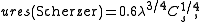
which corresponds to 6.1 nm−1 on the CM300. Contributions with a spatial frequency higher than the point resolution can be filtered out with an appropriate aperture leading to easily interpretable images at the cost of a lot of information lost.
Gabor defocus
Gabor defocus is used in electron holography where both amplitude and phase of the image wave are recorded. One thus wants to minimize crosstalk between the two. The Gabor defocus can be expressed as a function of the Scherzer defocus as
Lichte defocus
To exploit all beams transmitted through the microscope up to the information limit, one relies on a complex method called exit wave reconstruction which consists in mathematically reversing the effect of the CTF to recover the original exit wave φe(x,u). To maximize the information throughput, Hannes Lichte proposed in 1991 a defocus of a fundamentally different nature than the Scherzer defocus: because the dampening of the envelope function scales with the first derivative of χ(u), Lichte proposed a focus minimizing the modulus of dχ(u)/duwhere umax is the maximum transmitted spatial frequency. For the CM300 with an information limit of 0.8 Å Lichte defocus lies at −272 nm.
Exit wave reconstruction
First however, both phase and amplitude of the electron wave in the image plane must be measured. As our instruments only record amplitudes, an alternative method to recover the phase has to be used. There are two methods in use today:
- HolographyHolographyHolography is a technique that allows the light scattered from an object to be recorded and later reconstructed so that when an imaging system is placed in the reconstructed beam, an image of the object will be seen even when the object is no longer present...
, which was developed by GaborDennis GaborDennis Gabor CBE, FRS was a Hungarian-British electrical engineer and inventor, most notable for inventing holography, for which he later received the 1971 Nobel Prize in Physics....
expressly for TEM applications, uses a prism to split the beam into a reference beam and a second one passing through the sample. Phase changes between the two are then translated in small shifts of the interference pattern, which allows recovering both phase and amplitude of the interfering wave.
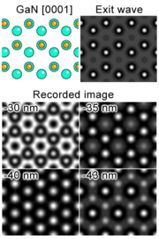
- Through focal series method takes advantage of the fact that the CTF is focus dependent. A series of about 20 pictures is shot under the same imaging conditions with the exception of the focus which is incremented between each take. Together with exact knowledge of the CTF the series allows for computation of φe(x,u) (see figure).
Both methods extend the point resolution of the microscope the information limit, which is the highest possible resolution achievable on a given machine. The ideal defocus value for this type of imaging is known as Lichte defocus and is usually several hundred nanometers negative.
See also
- Electron beam induced depositionElectron beam induced depositionElectron beam-induced deposition is a process of decomposing gaseous molecules by electron beam leading to deposition of non-volatile fragments onto a nearby substrate...
- Electron diffractionElectron diffractionElectron diffraction refers to the wave nature of electrons. However, from a technical or practical point of view, it may be regarded as a technique used to study matter by firing electrons at a sample and observing the resulting interference pattern...
- Electron energy loss spectroscopyElectron energy loss spectroscopyIn electron energy loss spectroscopy a material is exposed to a beam of electrons with a known, narrow range of kinetic energies. Some of the electrons will undergo inelastic scattering, which means that they lose energy and have their paths slightly and randomly deflected...
(EELS) - Electron microscopeElectron microscopeAn electron microscope is a type of microscope that uses a beam of electrons to illuminate the specimen and produce a magnified image. Electron microscopes have a greater resolving power than a light-powered optical microscope, because electrons have wavelengths about 100,000 times shorter than...
- Energy filtered transmission electron microscopyEnergy filtered transmission electron microscopyEnergy-filtered transmission electron microscopy is a technique used in Transmission electron microscopy, in which only electrons of particular kinetic energies are used to form the image or diffraction pattern...
(EFTEM) - Scanning confocal electron microscopyScanning confocal electron microscopyScanning confocal electron microscopy is an electron microscopy technique analogous to scanning confocal optical microscopy . In this technique, the studied sample is illuminated by a focussed electron beam, as in other scanning microscopy techniques, such as scanning transmission electron...
- Scanning electron microscopeScanning electron microscopeA scanning electron microscope is a type of electron microscope that images a sample by scanning it with a high-energy beam of electrons in a raster scan pattern...
(SEM) - Scanning transmission electron microscope (STEM)
- Transmission Electron MicroscopyTransmission electron microscopyTransmission electron microscopy is a microscopy technique whereby a beam of electrons is transmitted through an ultra thin specimen, interacting with the specimen as it passes through...
(TEM) - Transmission Electron Aberration-corrected MicroscopeTransmission Electron Aberration-corrected MicroscopeTransmission Electron Aberration-Corrected Microscope is a collaborative research project between four US laboratories and two companies. It is based at the Lawrence Berkeley National Laboratory in Berkeley, California and involves Argonne National Laboratory, Oak Ridge National Laboratory and...
Articles
- Topical review "Optics of high-performance electron Microscopes" Sci. Technol. Adv. Mater. 9 (2008) 014107 (30pages) free download
- CTF Explorer by Max V. Sidorov, freeware program to calculate the CTF
- High Resolution Transmission Electron Microscopy Overview