
Electron diffraction
Encyclopedia
Electron diffraction refers to the wave nature of electrons. However, from a technical or practical point of view, it may be regarded as a technique used to study matter by firing electrons at a sample and observing the resulting interference pattern. This phenomenon is commonly known as the wave-particle duality, which states that the behavior of a particle of matter (in this case the incident electron) can be described by a wave. For this reason, an electron can be regarded as a wave much like sound or water waves. This technique is similar to X-ray and neutron diffraction
.
Electron diffraction is most frequently used in solid state physics and chemistry to study the crystal structure
of solids. Experiments are usually performed in a transmission electron microscope
(TEM), or a scanning electron microscope
(SEM) as electron backscatter diffraction
. In these instruments, electrons are accelerated by an electrostatic potential in order to gain the desired energy and determine their wavelength before they interact with the sample to be studied.
The periodic structure of a crystalline solid acts as a diffraction grating
, scattering the electrons in a predictable manner. Working back from the observed diffraction pattern, it may be possible to deduce the structure of the crystal producing the diffraction pattern. However, the technique is limited by the phase problem
.
Apart from the study of crystals i.e. electron crystallography
, electron diffraction is also a useful technique to study the short range order of amorphous solids, and the geometry of gaseous molecules
.
George Paget Thomson
passed a beam of electrons through a thin metal film and observed the predicted interference patterns. At Bell Labs
Clinton Joseph Davisson and Lester Halbert Germer guided their beam through a crystalline grid. Thomson and Davisson shared the Nobel Prize for Physics in 1937 for their work.
s and neutron
s, electrons are charged particle
s and interact with matter through the Coulomb force
s. This means that the incident electrons feel the influence of both the positively charged atomic nuclei and the surrounding electrons. In comparison, X-rays interact with the spatial distribution of the valence electrons, while neutrons are scattered by the atomic nuclei through the strong nuclear forces. In addition, the magnetic moment
of neutrons is non-zero, and they are therefore also scattered by magnetic field
s. Because of these different forms of interaction, the three types of radiation are suitable for different studies.
Here is the wavefunction of the diffracted beam and
  is the so called structure factor
which is given by:

where is the scattering vector of the diffracted beam,
  is the position of an atom
  in the unit cell, and
  is the scattering power of the atom, also called the atomic form factor
. The sum is over all atoms in the unit cell.
The structure factor describes the way in which an incident beam of electrons is scattered by the atoms of a crystal unit cell, taking into account the different scattering power of the elements through the term . Since the atoms are spatially distributed in the unit cell, there will be a difference in phase when considering the scattered amplitude from two atoms. This phase shift is taken into account by the exponential term in the equation.
The atomic form factor, or scattering power, of an element depends on the type of radiation considered. Because electrons interact with matter though different processes than for example X-rays, the atomic form factors for the two cases are not the same.

Here is Planck's constant and
  the relativistic momentum of the electron.
  is called the de Broglie wavelength. The electrons are accelerated in an electric potential
  to the desired velocity:

 is the mass of the electron, and
  is the elementary charge.The electron wavelength is then given by:
However, in an electron microscope, the accelerating potential is usually several thousand volts causing the electron to travel at an appreciable fraction of the speed of light. An SEM may typically operate at an accelerating potential of 10,000 volts (10 kV) giving an electron velocity approximately 20% of the speed of light, while a typical TEM can operate at 200 kV raising the electron velocity to 70% the speed of light. We therefore need to take relativistic effects into account. It can be shown that the electron wavelength is then modified according to:
 is the speed of light. We recognize the first term in this final expression as the non-relativistic expression derived above, while the last term is a relativistic correction factor. The wavelength of the electrons in a 10 kV SEM is then 12.3 x 10⁻¹² m (12.3 pm) while in a 200 kV TEM the wavelength is 2.5 pm. In comparison the wavelength of X-rays usually used in X-ray diffraction is in the order of 100 pm (Cu kα: λ=154 pm).
(TEM) where the electrons pass through a thin film of the material to be studied. The resulting diffraction pattern is then observed on a fluorescent screen, recorded on photographic film, on imaging plates or using a CCD camera.
Furthermore, electron lenses allows the geometry of the diffraction experiment to be varied. The conceptually simplest geometry referred to as selected area electron diffraction (SAED) is that of a parallel beam of electrons incident on the specimen, with the specimen field selected using a sub-specimen image-plane aperture. However, by converging the electrons in a cone onto the specimen, one can in effect perform a diffraction experiment over several incident angles simultaneously. This technique is called Convergent Beam Electron Diffraction (CBED) and can reveal the full three dimensional symmetry of the crystal.
In a TEM, a single crystal grain or particle may be selected for the diffraction experiments. This means that the diffraction experiments can be performed on single crystals of nanometer size, whereas other diffraction techniques would be limited to studying the diffraction from a multicrystalline or powder sample. Furthermore, electron diffraction in TEM can be combined with direct imaging of the sample, including high resolution imaging of the crystal lattice, and a range of other techniques. These include solving and refining crystal structures by electron crystallography
, chemical analysis of the sample composition through energy-dispersive X-ray spectroscopy
, investigations of electronic structure and bonding through electron energy loss spectroscopy
, and studies of the mean inner potential through electron holography
.

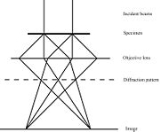
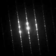 Figure 1 to the right is a simple sketch of the path of a parallel beam of electrons in a TEM from just above the sample and down the column to the fluorescent screen. As the electrons pass through the sample, they are scattered by the electrostatic potential set up by the constituent elements. After the electrons have left the sample they pass through the electromagnetic objective lens. This lens acts to collect all electrons scattered from one point of the sample in one point on the fluorescent screen, causing an image of the sample to be formed. We note that at the dashed line in the figure, electrons scattered in the same direction by the sample are collected into a single point. This is the back focal plane of the microscope, and is where the diffraction pattern is formed. By manipulating the magnetic lenses of the microscope, the diffraction pattern may be observed by projecting it onto the screen instead of the image. An example of what a diffraction pattern obtained in this way may look like is shown in figure 2.
If the sample is tilted with respect to the incident electron beam, one can obtain diffraction patterns from several crystal orientations. In this way, the reciprocal lattice
of the crystal can be mapped in three dimensions. By studying the systematic absence of diffraction spots the Bravais lattice and any screw axes
and glide plane
s present in the crystal structure may be determined.
The study of magnetic materials is complicated by the fact that electrons are deflected in magnetic fields by the Lorentz force
. Although this phenomenon may be exploited to study the magnetic domains of materials by Lorentz force microscopy, it may make crystal structure determination virtually impossible.
Furthermore, electron diffraction is often regarded as a qualitative technique suitable for symmetry determination, but too inaccurate for determination of lattice parameters and atomic positions. But there are also several examples where unknown crystal structures (both inorganic, organic and biological) have been solved by electron crystallography
. Lattice parameters of high accuracy can in fact be obtained from electron diffraction, relative errors less than 0.1% have been demonstrated. However, the right experimental conditions may be difficult to obtain, and these procedures are often viewed as too time consuming and the data too difficult to interpret. X-ray or neutron diffraction are therefore often the preferred methods for determining lattice parameters and atomic positions.
However, the main limitation of electron diffraction in TEM remains the comparatively high level of user interaction needed. Whereas both the execution of powder X-ray (and neutron) diffraction experiments and the data analysis are highly automated and routinely performed, electron diffraction requires a much higher level of user input.
Neutron diffraction
Neutron diffraction or elastic neutron scattering is the application of neutron scattering to the determination of the atomic and/or magnetic structure of a material: A sample to be examined is placed in a beam of thermal or cold neutrons to obtain a diffraction pattern that provides information of...
.
Electron diffraction is most frequently used in solid state physics and chemistry to study the crystal structure
Crystal structure
In mineralogy and crystallography, crystal structure is a unique arrangement of atoms or molecules in a crystalline liquid or solid. A crystal structure is composed of a pattern, a set of atoms arranged in a particular way, and a lattice exhibiting long-range order and symmetry...
of solids. Experiments are usually performed in a transmission electron microscope
Transmission electron microscopy
Transmission electron microscopy is a microscopy technique whereby a beam of electrons is transmitted through an ultra thin specimen, interacting with the specimen as it passes through...
(TEM), or a scanning electron microscope
Scanning electron microscope
A scanning electron microscope is a type of electron microscope that images a sample by scanning it with a high-energy beam of electrons in a raster scan pattern...
(SEM) as electron backscatter diffraction
Electron backscatter diffraction
Electron backscatter diffraction , also known as backscatter Kikuchi diffraction is a microstructural-crystallographic technique used to examine the crystallographic orientation of many materials, which can be used to elucidate texture or preferred orientation of any crystalline or polycrystalline...
. In these instruments, electrons are accelerated by an electrostatic potential in order to gain the desired energy and determine their wavelength before they interact with the sample to be studied.
The periodic structure of a crystalline solid acts as a diffraction grating
Diffraction grating
In optics, a diffraction grating is an optical component with a periodic structure, which splits and diffracts light into several beams travelling in different directions. The directions of these beams depend on the spacing of the grating and the wavelength of the light so that the grating acts as...
, scattering the electrons in a predictable manner. Working back from the observed diffraction pattern, it may be possible to deduce the structure of the crystal producing the diffraction pattern. However, the technique is limited by the phase problem
Phase problem
In physics the phase problem is the name given to the problem of loss of information concerning the phase that can occur when making a physical measurement. The name itself comes from the field of x-ray crystallography, where the phase problem has to be solved for the determination of a structure...
.
Apart from the study of crystals i.e. electron crystallography
Electron crystallography
Electron crystallography is a method to determine the arrangement of atoms in solids using a transmission electron microscope .- Comparison with X-ray crystallography :...
, electron diffraction is also a useful technique to study the short range order of amorphous solids, and the geometry of gaseous molecules
Gas electron diffraction
Gas electron diffraction is one of the applications of electron diffraction techniques. The target of this method is the determination of the structure of gaseous molecules i.e...
.
History
The de Broglie hypothesis, formulated in 1924, predicts that particles should also behave as waves. De Broglie's formula was confirmed three years later for electrons (which have a rest-mass) with the observation of electron diffraction in two independent experiments. At the University of AberdeenUniversity of Aberdeen
The University of Aberdeen, an ancient university founded in 1495, in Aberdeen, Scotland, is a British university. It is the third oldest university in Scotland, and the fifth oldest in the United Kingdom and wider English-speaking world...
George Paget Thomson
George Paget Thomson
Sir George Paget Thomson, FRS was an English physicist and Nobel laureate in physics recognised for his discovery with Clinton Davisson of the wave properties of the electron by electron diffraction.-Biography:...
passed a beam of electrons through a thin metal film and observed the predicted interference patterns. At Bell Labs
Bell Labs
Bell Laboratories is the research and development subsidiary of the French-owned Alcatel-Lucent and previously of the American Telephone & Telegraph Company , half-owned through its Western Electric manufacturing subsidiary.Bell Laboratories operates its...
Clinton Joseph Davisson and Lester Halbert Germer guided their beam through a crystalline grid. Thomson and Davisson shared the Nobel Prize for Physics in 1937 for their work.
Electron interaction with matter
Unlike other types of radiation used in diffraction studies of materials, such as X-rayX-ray
X-radiation is a form of electromagnetic radiation. X-rays have a wavelength in the range of 0.01 to 10 nanometers, corresponding to frequencies in the range 30 petahertz to 30 exahertz and energies in the range 120 eV to 120 keV. They are shorter in wavelength than UV rays and longer than gamma...
s and neutron
Neutron
The neutron is a subatomic hadron particle which has the symbol or , no net electric charge and a mass slightly larger than that of a proton. With the exception of hydrogen, nuclei of atoms consist of protons and neutrons, which are therefore collectively referred to as nucleons. The number of...
s, electrons are charged particle
Charged particle
In physics, a charged particle is a particle with an electric charge. It may be either a subatomic particle or an ion. A collection of charged particles, or even a gas containing a proportion of charged particles, is called a plasma, which is called the fourth state of matter because its...
s and interact with matter through the Coulomb force
Coulomb's law
Coulomb's law or Coulomb's inverse-square law, is a law of physics describing the electrostatic interaction between electrically charged particles. It was first published in 1785 by French physicist Charles Augustin de Coulomb and was essential to the development of the theory of electromagnetism...
s. This means that the incident electrons feel the influence of both the positively charged atomic nuclei and the surrounding electrons. In comparison, X-rays interact with the spatial distribution of the valence electrons, while neutrons are scattered by the atomic nuclei through the strong nuclear forces. In addition, the magnetic moment
Magnetic moment
The magnetic moment of a magnet is a quantity that determines the force that the magnet can exert on electric currents and the torque that a magnetic field will exert on it...
of neutrons is non-zero, and they are therefore also scattered by magnetic field
Magnetic field
A magnetic field is a mathematical description of the magnetic influence of electric currents and magnetic materials. The magnetic field at any given point is specified by both a direction and a magnitude ; as such it is a vector field.Technically, a magnetic field is a pseudo vector;...
s. Because of these different forms of interaction, the three types of radiation are suitable for different studies.
Intensity of diffracted beams
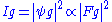
In the kinematical approximation for electron diffraction, the intensity of a diffracted beam is given by:Here
is the wavefunction of the diffracted beam and is the so called structure factorStructure factor
In condensed matter physics and crystallography, the static structure factor is a mathematical description of how a material scatters incident radiation...
which is given by:
where
is the scattering vector of the diffracted beam, is the position of an atom in the unit cell, and is the scattering power of the atom, also called the atomic form factorAtomic form factor
In physics, the atomic form factor, or atomic scattering factor, is a measure of the scattering amplitude of a wave by an isolated atom. The atomic form factor depends on the type of scattering, which in turn depends on the nature of the incident radiation, typically X-ray, electron or neutron...
. The sum is over all atoms in the unit cell.
The structure factor describes the way in which an incident beam of electrons is scattered by the atoms of a crystal unit cell, taking into account the different scattering power of the elements through the term
. Since the atoms are spatially distributed in the unit cell, there will be a difference in phase when considering the scattered amplitude from two atoms. This phase shift is taken into account by the exponential term in the equation.The atomic form factor, or scattering power, of an element depends on the type of radiation considered. Because electrons interact with matter though different processes than for example X-rays, the atomic form factors for the two cases are not the same.
Wavelength of electrons
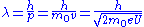
The wavelength of an electron is given by the de Broglie equationHere
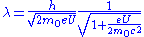
is Planck's constant and the relativistic momentum of the electron. is called the de Broglie wavelength. The electrons are accelerated in an electric potential to the desired velocity: is the mass of the electron, and is the elementary charge.The electron wavelength is then given by:However, in an electron microscope, the accelerating potential is usually several thousand volts causing the electron to travel at an appreciable fraction of the speed of light. An SEM may typically operate at an accelerating potential of 10,000 volts (10 kV) giving an electron velocity approximately 20% of the speed of light, while a typical TEM can operate at 200 kV raising the electron velocity to 70% the speed of light. We therefore need to take relativistic effects into account. It can be shown that the electron wavelength is then modified according to:
is the speed of light. We recognize the first term in this final expression as the non-relativistic expression derived above, while the last term is a relativistic correction factor. The wavelength of the electrons in a 10 kV SEM is then 12.3 x 10⁻¹² m (12.3 pm) while in a 200 kV TEM the wavelength is 2.5 pm. In comparison the wavelength of X-rays usually used in X-ray diffraction is in the order of 100 pm (Cu kα: λ=154 pm).Electron diffraction in a TEM
Electron diffraction of solids is usually performed in a Transmission Electron MicroscopeTransmission electron microscopy
Transmission electron microscopy is a microscopy technique whereby a beam of electrons is transmitted through an ultra thin specimen, interacting with the specimen as it passes through...
(TEM) where the electrons pass through a thin film of the material to be studied. The resulting diffraction pattern is then observed on a fluorescent screen, recorded on photographic film, on imaging plates or using a CCD camera.
Benefits
As mentioned above, the wavelength of electron accelerated in a TEM is much smaller than that of the radiation usually used for X-ray diffraction experiments. A consequence of this is that the radius of the Ewald sphere is much larger in electron diffraction experiments than in X-ray diffraction. This allows the diffraction experiment to reveal more of the two dimensional distribution of reciprocal lattice points.Furthermore, electron lenses allows the geometry of the diffraction experiment to be varied. The conceptually simplest geometry referred to as selected area electron diffraction (SAED) is that of a parallel beam of electrons incident on the specimen, with the specimen field selected using a sub-specimen image-plane aperture. However, by converging the electrons in a cone onto the specimen, one can in effect perform a diffraction experiment over several incident angles simultaneously. This technique is called Convergent Beam Electron Diffraction (CBED) and can reveal the full three dimensional symmetry of the crystal.
In a TEM, a single crystal grain or particle may be selected for the diffraction experiments. This means that the diffraction experiments can be performed on single crystals of nanometer size, whereas other diffraction techniques would be limited to studying the diffraction from a multicrystalline or powder sample. Furthermore, electron diffraction in TEM can be combined with direct imaging of the sample, including high resolution imaging of the crystal lattice, and a range of other techniques. These include solving and refining crystal structures by electron crystallography
Electron crystallography
Electron crystallography is a method to determine the arrangement of atoms in solids using a transmission electron microscope .- Comparison with X-ray crystallography :...
, chemical analysis of the sample composition through energy-dispersive X-ray spectroscopy
Energy-dispersive X-ray spectroscopy
Energy-dispersive X-ray spectroscopy is an analytical technique used for the elemental analysis or chemical characterization of a sample. It relies on the investigation of an interaction of a some source of X-ray excitation and a sample...
, investigations of electronic structure and bonding through electron energy loss spectroscopy
Electron energy loss spectroscopy
In electron energy loss spectroscopy a material is exposed to a beam of electrons with a known, narrow range of kinetic energies. Some of the electrons will undergo inelastic scattering, which means that they lose energy and have their paths slightly and randomly deflected...
, and studies of the mean inner potential through electron holography
Electron holography
Electron holography is holography with electron waves. Dennis Gabor invented holography in 1948 when he tried to improve resolution in electron microscope. The first attempts to perform holography with electron waves were made by Haine and Muley in 1952; they demonstrated recorded with 60keV...
.
Practical aspects
If the sample is tilted with respect to the incident electron beam, one can obtain diffraction patterns from several crystal orientations. In this way, the reciprocal lattice
Reciprocal lattice
In physics, the reciprocal lattice of a lattice is the lattice in which the Fourier transform of the spatial function of the original lattice is represented. This space is also known as momentum space or less commonly k-space, due to the relationship between the Pontryagin duals momentum and...
of the crystal can be mapped in three dimensions. By studying the systematic absence of diffraction spots the Bravais lattice and any screw axes
Screw axis
The screw axis of an object is a line that is simultaneously the axis of rotation and the line along which a translation occurs...
and glide plane
Glide plane
In crystallography, a glide plane is symmetry operation describing how a reflection in a plane, followed by a translation parallel with that plane, may leave the crystal unchanged....
s present in the crystal structure may be determined.
Limitations
Electron diffraction in TEM is subject to several important limitations. First, the sample to be studied must be electron transparent, meaning the sample thickness must be of the order of 100 nm or less. Careful and time consuming sample preparation may therefore be needed. Furthermore, many samples are vulnerable to radiation damage caused by the incident electrons.The study of magnetic materials is complicated by the fact that electrons are deflected in magnetic fields by the Lorentz force
Lorentz force
In physics, the Lorentz force is the force on a point charge due to electromagnetic fields. It is given by the following equation in terms of the electric and magnetic fields:...
. Although this phenomenon may be exploited to study the magnetic domains of materials by Lorentz force microscopy, it may make crystal structure determination virtually impossible.
Furthermore, electron diffraction is often regarded as a qualitative technique suitable for symmetry determination, but too inaccurate for determination of lattice parameters and atomic positions. But there are also several examples where unknown crystal structures (both inorganic, organic and biological) have been solved by electron crystallography
Electron crystallography
Electron crystallography is a method to determine the arrangement of atoms in solids using a transmission electron microscope .- Comparison with X-ray crystallography :...
. Lattice parameters of high accuracy can in fact be obtained from electron diffraction, relative errors less than 0.1% have been demonstrated. However, the right experimental conditions may be difficult to obtain, and these procedures are often viewed as too time consuming and the data too difficult to interpret. X-ray or neutron diffraction are therefore often the preferred methods for determining lattice parameters and atomic positions.
However, the main limitation of electron diffraction in TEM remains the comparatively high level of user interaction needed. Whereas both the execution of powder X-ray (and neutron) diffraction experiments and the data analysis are highly automated and routinely performed, electron diffraction requires a much higher level of user input.
See also
- Electron microscopeElectron microscopeAn electron microscope is a type of microscope that uses a beam of electrons to illuminate the specimen and produce a magnified image. Electron microscopes have a greater resolving power than a light-powered optical microscope, because electrons have wavelengths about 100,000 times shorter than...
- Transmission electron microscopyTransmission electron microscopyTransmission electron microscopy is a microscopy technique whereby a beam of electrons is transmitted through an ultra thin specimen, interacting with the specimen as it passes through...
- Selected area diffractionSelected area diffractionSelected area diffraction , is a crystallographic experimental technique that can be performed inside a transmission electron microscope ....
- Gas electron diffractionGas electron diffractionGas electron diffraction is one of the applications of electron diffraction techniques. The target of this method is the determination of the structure of gaseous molecules i.e...
- RHEEDRHEEDReflection high-energy electron diffraction is a technique used to characterize the surface of crystalline materials. RHEED systems gather information only from the surface layer of the sample, which distinguishes RHEED from other materials characterization methods that also rely on diffraction of...
- Low-energy electron diffraction
- Stereographic projectionStereographic projectionThe stereographic projection, in geometry, is a particular mapping that projects a sphere onto a plane. The projection is defined on the entire sphere, except at one point — the projection point. Where it is defined, the mapping is smooth and bijective. It is conformal, meaning that it...
- Kikuchi lineKikuchi lineKikuchi lines pair up to form bands in electron diffraction from single crystal specimens, there to serve as "roads in orientation-space" for microscopists not sure what they are looking at. In transmission electron microscopes, they are easily seen in diffraction from regions of the specimen thick...
- Electron backscatter diffractionElectron backscatter diffractionElectron backscatter diffraction , also known as backscatter Kikuchi diffraction is a microstructural-crystallographic technique used to examine the crystallographic orientation of many materials, which can be used to elucidate texture or preferred orientation of any crystalline or polycrystalline...
External links
- Remote experiment on electron diffraction (choose English and then "Labs")
- JmolJmolJmol is an open-source Java viewer for chemical structures in 3D,that does not require 3D acceleration plugins.Jmol returns a 3D representation of a molecule that may be used as a teaching tool, or for research e.g...
-mediated image/diffraction analysis of an unknown