
Double patterning
Encyclopedia
Multiple patterning is a class of technologies for manufacturing integrated circuits (ICs), developed for photolithography
to enhance the feature density. The simplest case of multiple patterning is double patterning, where a conventional lithography process is enhanced to produce double the expected number of features. The resolution of a photoresist pattern begins to blur at around 45 nm half-pitch. For the semiconductor industry
, therefore, double patterning was introduced for the 32 nm half-pitch node and below, mainly using state-of-the-art 193 nm immersion lithography
tools.
There are several types of double patterning. In combination, these may be used for multiple patterning.
 A spacer is a film layer formed on the sidewall of a pre-patterned feature. A spacer is formed by deposition or reaction of the film on the previous pattern, followed by etching to remove all the film material on the horizontal surfaces, leaving only the material on the sidewalls. By removing the original patterned feature, only the spacer is left. However, since there are two spacers for every line, the line density has now doubled. The spacer technique is applicable for defining narrow gates at half the original lithographic pitch, for example.
The spacer approach is unique in that with one lithographic exposure, the pitch can be halved indefinitely with a succession of spacer formation and pattern transfer processes. This conveniently avoids the serious issue of overlay between successive exposures. The spacer lithography technique has most frequently been applied in patterning fins for FinFETs.
As spacer materials are commonly hardmask
materials, their post-etch pattern quality tends to be superior compared to photoresist profiles after etch, which are generally plagued by line edge roughness.
The main issues with the spacer approach are whether the spacers can stay in place after the material to which they are attached is removed, whether the spacer profile is acceptable, and whether the underlying material is attacked by the etch removing the material attached to the spacer. Pattern transfer is complicated by the situation where removal of the material adjacent to the spacers also removes a little of the underlying material. This results in higher topography on one side of the spacer than the other.
The positioning of the spacer also depends on the pattern to which the spacer is attached. If the pattern is too wide or too narrow, the spacer position is affected. However, this would not be a concern for critical memory feature fabrication processes which are self-aligned.
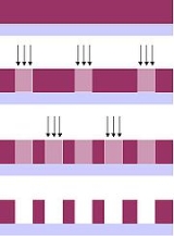
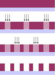 Double exposure is a sequence of two separate exposures of the same photoresist
layer using two different photomask
s. This technique is commonly used for patterns in the same layer which look very different or have incompatible densities or pitches. In one important case, the two exposures may each consist of lines which are oriented in one or the other of two usually perpendicular directions. This allows the decomposition of two-dimensional patterns into two one-dimensional patterns which are easier to print. This is the basis of DDL technology from Brion Technologies, a subsidiary of ASML
. The sum of the exposures cannot improve the minimum resolution limit unless the photoresist response is not a simple addition of the two exposures. The double exposure technique allows manufacturability of minimum pitch features in a layout that may contain a variety of features. The 65 nm node saw the introduction of alternating phase-shift masks in manufacturing. This technology is typically a double exposure approach. As long as double exposure can be used effectively and is kept within alignment tolerances, it is the preferred patterning approach since it does not require additional follow-up process steps.
Direct-write electron-beam lithography is inherently a multiple exposure technique, as the beam is shaped and projected onto the resist at multiple locations.
) recently used this approach to pattern the gate level for its 32 nm half-pitch demonstration.
A concern with the use of this approach is the discrepancy and delay between the second photoresist pattern and the first hardmask pattern, resulting in an additional source of variation.
A variation on this approach which eliminates the first hardmask etch is resist freezing, which allows a second resist coating over the first developed resist layer. JSR has demonstrated 32 nm lines and spaces using this method, where the freezing is accomplished by surface hardening of the first resist layer.
A possible application would be, for example, dividing the contact layer into two separate groups: gate contacts and source/drain contacts, each defining its own mask. IMEC recently used an approach like this to demonstrate a 45 nm
node 6-transistor SRAM cell using dry lithography http://www.reed-electronics.com/semiconductor/article/CA604512.
As with the double-expose, double-etch mesas approach, any discrepancy among the different interleaved patterns would be a source of feature-to-feature variation.
Beyond double (2X) patterning, the most frequently published multiple patterning methodology is the repeated spacer approach, which can be practiced in many forms. A multilayer-on-topography spacer-type approach also offers some flexibility. It is also possible to additively combine two or more of the above approaches. For example, a dual-tone photoresist with pitch-halved acid profile, plus dual-tone development that dissolves the highest and lowest acid concentrations, combined with a spacer process, would result in 8x pitch resolution enhancement,e.g., 40 nm half-pitch reduced to 5 nm half-pitch. Subsequently repeating the spacer process would give 16 x pitch resolution improvement, e.g., 40 nm half-pitch reduced to 2.5 nm half-pitch. The European LENS (Lithography Enhancement Towards Nano Scale) project is targeted toward implementation of both double exposure (resist freezing) and spacer-based process, in principle enabling two ways of patterning for ~20 nm design rules with current lithography tools, already tailored for double patterning or ~10 nm design rules in combination. With successful dual-tone development of a dual-tone photoresist, 2.5 nm design rules can be imagined.
Intel used several spacer deposition/etch/clean steps to demonstrate spacers spaced apart by ~26 nm. It represents a reduction of the original patterned pitch by a factor of ~1/4 and indicates that wavelength and optics no longer purely determine the lithographic resolution.
IMEC
has indicated that in the event that EUV lithography is not ready, quadruple patterning (with tighter overlay specifications) would be used.
At the 2010 Flash Memory Summit, it was projected that immersion lithography with multiple patterning would be used to scale NAND Flash to below 20 nm within a few years.
Synopsys
has begun consideration of triple patterning decomposition of layers which are less easy to split into two patterns, such as contact layers. While only increasing the number of processing steps by 50% (compared to 100% for the insertion of double patterning), triple patterning would enable 16 nm node patterning on a 45 nm node lithography tool. Likewise, quadruple patterning would enable 11 nm node patterning on the same 45 nm node lithography tool, with only 33% additional steps over triple patterning.
techniques such as EUVL and nanoimprint lithography
.
Multiple patterning can also exploit high-bias processes (for example, photoresist trimming to reduce linewidth, or photoresist reflow to reduce trench width) to substantially eliminate defects sized at around 2x the design pitch or smaller. This is a significant advantage over increasing lithography tool resolution, which exposes the wafer to more defects at the design rule or even smaller.
in 3D-ICs, requires patterning each die sequentially, as well as multiple instances of through-silicon via
patterning.
would eventually require at least two interleaved exposures (due to secondary electron scattering), for instance, in the fabrication of 15 nm half-pitch X-ray zone plates. In fact, double patterning may not even be sufficient for sub-12 nm half-pitch, even with electron beam lithography. In that case, multiple patterning would be necessary.
In September 2009, Intel disclosed that for its 15 nm process, EUV did not appear to be ready in timely fashion. Hence, Intel is preparing to extend 193 nm immersion lithography with double and possibly triple patterning to 15 nm.
For its 11 nm logic node (20-22 nm half-pitch), Intel expects to be able to use quintuple exposure with 193 nm lithography, where one of the exposures is used with spacer patterning for a further pitch division. The remaining four exposures are for cutting the pitch-divided lines. Even with a next-generation lithography like EUVL or maskless
direct-write electron-beam lithography, a second exposure is still required for cutting. Referenced to its 32 nm node technology, the density is expected to be enhanced about 8x (three generations of doubling density), but the cost is less than 6x (5 exposures, with one round of spacer patterning).
Similar to the multiple patterning approach described for Intel's 11 nm process, in actual practice, NAND Flash memory
array patterning using the spacer approach would use 3 or more mask exposures. The first mask patterns the array core by defining the spacers, while a second mask is used to crop or trim the spacers to form individual lines. Lastly, additional masks or multiple patterning would be used to pattern peripheral connections, e.g., pads. As a result, Flash memory patterning can generally be considered multiple patterning, not just a spacer-based double-patterning technique.
At IEDM 2011, Hynix is expected to report on a 15 nm NAND process, making use of, among other things, quadruple spacer patterning.
Photolithography
Photolithography is a process used in microfabrication to selectively remove parts of a thin film or the bulk of a substrate. It uses light to transfer a geometric pattern from a photomask to a light-sensitive chemical "photoresist", or simply "resist," on the substrate...
to enhance the feature density. The simplest case of multiple patterning is double patterning, where a conventional lithography process is enhanced to produce double the expected number of features. The resolution of a photoresist pattern begins to blur at around 45 nm half-pitch. For the semiconductor industry
Semiconductor industry
The semiconductor industry is the aggregate collection of companies engaged in the design and fabrication of semiconductor devices. It formed around 1960, once the fabrication of semiconductors became a viable business...
, therefore, double patterning was introduced for the 32 nm half-pitch node and below, mainly using state-of-the-art 193 nm immersion lithography
Immersion lithography
Immersion lithography is a photolithography resolution enhancement technique for manufacturing integrated circuits that replaces the usual air gap between the final lens and the wafer surface with a liquid medium that has a refractive index greater than one. The resolution is increased by a factor...
tools.
There are several types of double patterning. In combination, these may be used for multiple patterning.
Dual-tone photoresist
Dual-tone photoresists have been developed years ago, allowing the printing of two lines in a single exposure imaging of a single line. Early demonstrations relied on crosslinking of the highest dose regions, rendering them insoluble in developer, while the lowest dose regions were normally insoluble already. Alternatively, a photobase generator may generate acid quenchers at high doses; the acid quenching counters their ability to render the photoresist soluble. The simplicity and cost-effectiveness of this approach make it compelling as a method of extending current photolithographic capability. However, due to its inherent edge-printing characteristic, loops will generally be formed, which will need to be addressed by other process steps. In addition, the expected acid or base diffusion may limit the resolution of this technique.Dual-Tone Development
Dual-tone development, such as Fujifilm's double development process, is similar to the dual-tone photoresist technique above in that it doubles features without additional exposure. Instead the photoresist is developed twice; the first time by conventional developer which removes the high exposure dose areas, the second time by a different organic solvent which removes the unexposed or lowest exposure dose areas. This leaves the intermediate dose areas (normally defining the two feature edges) standing. A key challenge is to not only show successful positive and negative tone development process windows, but also to ensure the windows overlap sufficiently. Up to now, the successful overlap has only been shown in simulations rather than experimentally.Self-aligned spacer
The spacer approach is unique in that with one lithographic exposure, the pitch can be halved indefinitely with a succession of spacer formation and pattern transfer processes. This conveniently avoids the serious issue of overlay between successive exposures. The spacer lithography technique has most frequently been applied in patterning fins for FinFETs.
As spacer materials are commonly hardmask
Hardmask
A hardmask is a material used in semiconductor processing as an etch mask in lieu of polymer or other organic "soft" resist materials. The idea is that polymers tend to be etched easily by oxygen, fluorine, chlorine or other reactive gases to the extent that a pattern defined using polymeric mask...
materials, their post-etch pattern quality tends to be superior compared to photoresist profiles after etch, which are generally plagued by line edge roughness.
The main issues with the spacer approach are whether the spacers can stay in place after the material to which they are attached is removed, whether the spacer profile is acceptable, and whether the underlying material is attacked by the etch removing the material attached to the spacer. Pattern transfer is complicated by the situation where removal of the material adjacent to the spacers also removes a little of the underlying material. This results in higher topography on one side of the spacer than the other.
The positioning of the spacer also depends on the pattern to which the spacer is attached. If the pattern is too wide or too narrow, the spacer position is affected. However, this would not be a concern for critical memory feature fabrication processes which are self-aligned.
Double/Multiple exposure
Photoresist
A photoresist is a light-sensitive material used in several industrial processes, such as photolithography and photoengraving to form a patterned coating on a surface.-Tone:Photoresists are classified into two groups: positive resists and negative resists....
layer using two different photomask
Photomask
A photomask is an opaque plate with holes or transparencies that allow light to shine through in a defined pattern. They are commonly used in photolithography.-Overview:...
s. This technique is commonly used for patterns in the same layer which look very different or have incompatible densities or pitches. In one important case, the two exposures may each consist of lines which are oriented in one or the other of two usually perpendicular directions. This allows the decomposition of two-dimensional patterns into two one-dimensional patterns which are easier to print. This is the basis of DDL technology from Brion Technologies, a subsidiary of ASML
ASML Holding
ASML is a Dutch company and the largest supplier in the world of photolithography systems for the semiconductor industry. The company manufactures machines for the production of integrated circuits , such as RAM and flash memory chips and CPUs.-Products:...
. The sum of the exposures cannot improve the minimum resolution limit unless the photoresist response is not a simple addition of the two exposures. The double exposure technique allows manufacturability of minimum pitch features in a layout that may contain a variety of features. The 65 nm node saw the introduction of alternating phase-shift masks in manufacturing. This technology is typically a double exposure approach. As long as double exposure can be used effectively and is kept within alignment tolerances, it is the preferred patterning approach since it does not require additional follow-up process steps.
Direct-write electron-beam lithography is inherently a multiple exposure technique, as the beam is shaped and projected onto the resist at multiple locations.
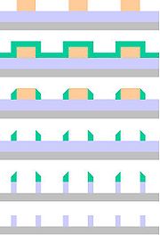
Double Expose, Double Etch (mesas)
This is best described by considering a process example. A first exposure of photoresist is transferred to an underlying hardmask layer. After the photoresist is removed following the hardmask pattern transfer, a second layer of photoresist is coated onto the sample and this layer undergoes a second exposure, imaging features in between the features patterned in the hardmask layer. The surface pattern is made up of photoresist features edged between mask features, which can be transferred into the final layer underneath. This allows a doubling of feature density. The Interuniversity Microelectronics Centre (IMEC, BelgiumBelgium
Belgium , officially the Kingdom of Belgium, is a federal state in Western Europe. It is a founding member of the European Union and hosts the EU's headquarters, and those of several other major international organisations such as NATO.Belgium is also a member of, or affiliated to, many...
) recently used this approach to pattern the gate level for its 32 nm half-pitch demonstration.
A concern with the use of this approach is the discrepancy and delay between the second photoresist pattern and the first hardmask pattern, resulting in an additional source of variation.
A variation on this approach which eliminates the first hardmask etch is resist freezing, which allows a second resist coating over the first developed resist layer. JSR has demonstrated 32 nm lines and spaces using this method, where the freezing is accomplished by surface hardening of the first resist layer.
Double Expose, Double Etch (trenches)
A "brute force" approach for patterning trenches involves a sequence of (at least) two separate exposures and etchings of independent patterns into the same layer. For each exposure, a different photoresist coating is required. When the sequence is completed, the pattern is a composite of the previously etched subpatterns. By interleaving the subpatterns, the pattern density can theoretically be increased indefinitely, the half-pitch being inversely proportional to the number of subpatterns used. For example, a 25 nm half-pitch pattern can be generated from interleaving two 50 nm half-pitch patterns, three 75 nm half-pitch patterns, or four 100 nm half-pitch patterns. The feature size reduction will most likely require the assistance of techniques such as chemical shrinks, thermal reflow, or shrink assist films. This composite pattern can then be transferred down into the final layer.A possible application would be, for example, dividing the contact layer into two separate groups: gate contacts and source/drain contacts, each defining its own mask. IMEC recently used an approach like this to demonstrate a 45 nm
45 nanometer
Per the International Technology Roadmap for Semiconductors, the 45 nm technology node should refer to the average half-pitch of a memory cell manufactured at around the 2007–2008 time frame....
node 6-transistor SRAM cell using dry lithography http://www.reed-electronics.com/semiconductor/article/CA604512.
As with the double-expose, double-etch mesas approach, any discrepancy among the different interleaved patterns would be a source of feature-to-feature variation.
Multiple patterning - the ultimate resolution
The extrapolation of double patterning to multiple patterning has been contemplated, but the issue of cost control is still on the minds of many. While the benefits of multiple patterning in terms of resolution, depth of focus and lithographic defect sensitivity are understood, there is added burden to control the process budget increase and maintain good yield.Beyond double (2X) patterning, the most frequently published multiple patterning methodology is the repeated spacer approach, which can be practiced in many forms. A multilayer-on-topography spacer-type approach also offers some flexibility. It is also possible to additively combine two or more of the above approaches. For example, a dual-tone photoresist with pitch-halved acid profile, plus dual-tone development that dissolves the highest and lowest acid concentrations, combined with a spacer process, would result in 8x pitch resolution enhancement,e.g., 40 nm half-pitch reduced to 5 nm half-pitch. Subsequently repeating the spacer process would give 16 x pitch resolution improvement, e.g., 40 nm half-pitch reduced to 2.5 nm half-pitch. The European LENS (Lithography Enhancement Towards Nano Scale) project is targeted toward implementation of both double exposure (resist freezing) and spacer-based process, in principle enabling two ways of patterning for ~20 nm design rules with current lithography tools, already tailored for double patterning or ~10 nm design rules in combination. With successful dual-tone development of a dual-tone photoresist, 2.5 nm design rules can be imagined.
Intel used several spacer deposition/etch/clean steps to demonstrate spacers spaced apart by ~26 nm. It represents a reduction of the original patterned pitch by a factor of ~1/4 and indicates that wavelength and optics no longer purely determine the lithographic resolution.
IMEC
Imec
Imec is a micro- and nanoelectronics research center headquartered in Leuven, Belgium, with offices in Belgium, the Netherlands, Taiwan, USA, China and Japan. Its staff of about 1,900 people includes more than 500 industrial residents and guest researchers...
has indicated that in the event that EUV lithography is not ready, quadruple patterning (with tighter overlay specifications) would be used.
At the 2010 Flash Memory Summit, it was projected that immersion lithography with multiple patterning would be used to scale NAND Flash to below 20 nm within a few years.
2D layout considerations
For 2D patterns the density increase is very dependent on the nature of the pattern. For instance, contact arrays have optimal packing density as rectangular arrays for double patterning but as hexagonal close packed arrays for triple patterning – achieving a close to 2 and 3 times area improvement respectively. For 2D layouts double patterning compliance errors occur when there are odd cycles of minimum spaces. This can be resolved by relaxing one of these spaces to a distance where both features can be patterned in the same imaging step. Triple patterning is compliant with odd cycles but in turn is non-complaint for two facing pairs of line-ends where the corner to corner space is below the single patterning distance. This in turn is compliant under quadruple patterning. The improvement in density with the use of multiple patterning schemes is thus highly dependent on the pattern. Often simple redesigns or relaxation of dimensions in one direction can avoid the expense of going to more complex and expensive multiple patterning processes.Synopsys
Synopsys
Synopsys, Inc. is one of the largest companies in the Electronic Design Automation industry. Synopsys' first and best-known product is Design Compiler, a logic-synthesis tool. Synopsys offers a wide range of other products used in the design of an application-specific integrated circuit...
has begun consideration of triple patterning decomposition of layers which are less easy to split into two patterns, such as contact layers. While only increasing the number of processing steps by 50% (compared to 100% for the insertion of double patterning), triple patterning would enable 16 nm node patterning on a 45 nm node lithography tool. Likewise, quadruple patterning would enable 11 nm node patterning on the same 45 nm node lithography tool, with only 33% additional steps over triple patterning.
Implementations
Due to its rather straightforward application, without the need to change the infrastructure, multiple patterning is not expected to encounter any insurmountable technical or commercialization barriers. Despite the cost and throughput concerns, it has recently received more attention and interest, mainly due to delays in next-generation lithographyNext-generation lithography
Next-generation lithography is a term used in integrated circuit manufacturing to describe the lithography technologies slated to replace photolithography. As of 2009 the most advanced form of photolithography is immersion lithography, in which water is used as an immersion medium for the final...
techniques such as EUVL and nanoimprint lithography
Nanoimprint Lithography
Nanoimprint lithography is a method of fabricating nanometer scale patterns. It is a simple nanolithography process with low cost, high throughput and high resolution. It creates patterns by mechanical deformation of imprint resist and subsequent processes. The imprint resist is typically a monomer...
.
Multiple patterning can also exploit high-bias processes (for example, photoresist trimming to reduce linewidth, or photoresist reflow to reduce trench width) to substantially eliminate defects sized at around 2x the design pitch or smaller. This is a significant advantage over increasing lithography tool resolution, which exposes the wafer to more defects at the design rule or even smaller.
Chip stacking of multiple dice
Stacking of multiple dice, e.g., DRAMDram
Dram or DRAM may refer to:As a unit of measure:* Dram , an imperial unit of mass and volume* Armenian dram, a monetary unit* Dirham, a unit of currency in several Arab nationsOther uses:...
in 3D-ICs, requires patterning each die sequentially, as well as multiple instances of through-silicon via
Through-silicon via
In electronic engineering, a through-silicon via is a vertical electrical connection passing completely through a silicon wafer or die...
patterning.
Electron-beam lithography
As mentioned above, electron-beam lithography is inherently a multiple exposure technique. However, even electron beam lithographyElectron beam lithography
Electron beam lithography is the practice of emitting a beam of electrons in a patterned fashion across a surface covered with a film , and of selectively removing either exposed or non-exposed regions of the resist...
would eventually require at least two interleaved exposures (due to secondary electron scattering), for instance, in the fabrication of 15 nm half-pitch X-ray zone plates. In fact, double patterning may not even be sufficient for sub-12 nm half-pitch, even with electron beam lithography. In that case, multiple patterning would be necessary.
Tela Innovations
Tela Innovations, a startup founded in 2005 which has recently garnered significant support and funding, specializes in converting arbitrary layouts into array-like features suitable for double patterning. Tela Innovations achieves this by using gridded layouts (see Figures).Intel
Intel has been using double patterning in its 45 nm as well as its 65 nm technology. Double patterning is used to square off the ends of the transistor gates. The first mask pattern consists of the gate lines linked at the end. The second mask is a line cutter that separates these into separate gates, using a second photoresist coating. The extra steps for the 45 nm double patterning compared to 65 nm are necessary due to the use of dry instead of immersion lithography.In September 2009, Intel disclosed that for its 15 nm process, EUV did not appear to be ready in timely fashion. Hence, Intel is preparing to extend 193 nm immersion lithography with double and possibly triple patterning to 15 nm.
For its 11 nm logic node (20-22 nm half-pitch), Intel expects to be able to use quintuple exposure with 193 nm lithography, where one of the exposures is used with spacer patterning for a further pitch division. The remaining four exposures are for cutting the pitch-divided lines. Even with a next-generation lithography like EUVL or maskless
Maskless lithography
In maskless lithography, the radiation that is used to expose a photosensitive emulsion is not projected from, or transmitted through, a photomask. Instead, most commonly, the radiation is focused to a narrow beam. The beam is then used to directly write the image into the photoresist, one or more...
direct-write electron-beam lithography, a second exposure is still required for cutting. Referenced to its 32 nm node technology, the density is expected to be enhanced about 8x (three generations of doubling density), but the cost is less than 6x (5 exposures, with one round of spacer patterning).
Texas Instruments
At the 2010 Sematech Litho Forum, it was recommended by TI that for the 60 nm routed pitch layers, corresponding to the 22/20 nm node, double patterning “is the only economically feasible solution." Double and triple patterning was considered cost effective for dice with a routed pitch of about 40nm. For the 14nm node, triple patterning will be required for the gate, contact, and metal 1 layers. It was claimed that triple patterning at the 44 nm pitch provided a 25% better cost reduction.NAND Flash Memory Makers
In 2010, IM Flash began producing 25 nm NAND Flash, with the combination of 193 nm immersion lithography and double patterning.Similar to the multiple patterning approach described for Intel's 11 nm process, in actual practice, NAND Flash memory
Flash memory
Flash memory is a non-volatile computer storage chip that can be electrically erased and reprogrammed. It was developed from EEPROM and must be erased in fairly large blocks before these can be rewritten with new data...
array patterning using the spacer approach would use 3 or more mask exposures. The first mask patterns the array core by defining the spacers, while a second mask is used to crop or trim the spacers to form individual lines. Lastly, additional masks or multiple patterning would be used to pattern peripheral connections, e.g., pads. As a result, Flash memory patterning can generally be considered multiple patterning, not just a spacer-based double-patterning technique.
At IEDM 2011, Hynix is expected to report on a 15 nm NAND process, making use of, among other things, quadruple spacer patterning.