
Intel 82497
Encyclopedia
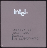
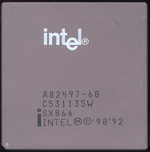
The Intel 82497 is a Cache Controller for the Pentium
processor. It works with multiple 82492 Cache SRAMs.
The 82497 Cache Controller with multiple 82492 Cache SRAMs combine with the Pentium
processor (735\90,815\100, 1000\120, 1110\133) to form a CPU cache chip set designed for high performance servers and function-rich desktops. The high-speed interconnect between the CPU and cache components has been optimized to provide zero-wait state operation. This CPU cache chip set is fully compatible with existing software, and has data integrity features for mission critical applications.
The 82497 Cache Controller implements the MESI write-back protocol for full multiprocessing support. Dual ported buffers and registers allow the 82497 to concurrently handle CPU bus, memory bus, and internal cache operation for maximum performance. The 82492 is a customized high performance SRAM that supports 32-, 64-, and 128-bit
wide memory bus widths, 16-, 32-, and 64-byte line sizes, and optional sectoring. The data path between the CPU bus and the memory bus is separated by the 82492, allowing the CPU bus to handshake synchronously, asynchronously, or with a strobed protocol, and allowing concurrent CPU bus and memory bus operations.
Pentium
The original Pentium microprocessor was introduced on March 22, 1993. Its microarchitecture, deemed P5, was Intel's fifth-generation and first superscalar x86 microarchitecture. As a direct extension of the 80486 architecture, it included dual integer pipelines, a faster FPU, wider data bus,...
processor. It works with multiple 82492 Cache SRAMs.
Technical description
The 82497 Cache Controller implements the MESI write-back protocol for full multiprocessing support. Dual ported buffers and registers allow the 82497 to concurrently handle CPU bus, memory bus, and internal cache operation for maximum performance.The 82497 Cache Controller with multiple 82492 Cache SRAMs combine with the Pentium
Pentium
The original Pentium microprocessor was introduced on March 22, 1993. Its microarchitecture, deemed P5, was Intel's fifth-generation and first superscalar x86 microarchitecture. As a direct extension of the 80486 architecture, it included dual integer pipelines, a faster FPU, wider data bus,...
processor (735\90,815\100, 1000\120, 1110\133) to form a CPU cache chip set designed for high performance servers and function-rich desktops. The high-speed interconnect between the CPU and cache components has been optimized to provide zero-wait state operation. This CPU cache chip set is fully compatible with existing software, and has data integrity features for mission critical applications.
The 82497 Cache Controller implements the MESI write-back protocol for full multiprocessing support. Dual ported buffers and registers allow the 82497 to concurrently handle CPU bus, memory bus, and internal cache operation for maximum performance. The 82492 is a customized high performance SRAM that supports 32-, 64-, and 128-bit
wide memory bus widths, 16-, 32-, and 64-byte line sizes, and optional sectoring. The data path between the CPU bus and the memory bus is separated by the 82492, allowing the CPU bus to handshake synchronously, asynchronously, or with a strobed protocol, and allowing concurrent CPU bus and memory bus operations.