

Contact pad
Encyclopedia
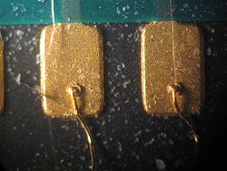
Contact pads are designated surface areas of a printed circuit board
Printed circuit board
A printed circuit board, or PCB, is used to mechanically support and electrically connect electronic components using conductive pathways, tracks or signal traces etched from copper sheets laminated onto a non-conductive substrate. It is also referred to as printed wiring board or etched wiring...
or die
Die (integrated circuit)
A die in the context of integrated circuits is a small block of semiconducting material, on which a given functional circuit is fabricated.Typically, integrated circuits are produced in large batches on a single wafer of electronic-grade silicon or other semiconductor through processes such as...
of an integrated circuit
Integrated circuit
An integrated circuit or monolithic integrated circuit is an electronic circuit manufactured by the patterned diffusion of trace elements into the surface of a thin substrate of semiconductor material...
. Possibilities to contact to pads include solder
Solder
Solder is a fusible metal alloy used to join together metal workpieces and having a melting point below that of the workpiece.Soft solder is what is most often thought of when solder or soldering are mentioned and it typically has a melting range of . It is commonly used in electronics and...
ing, wirebonding
Wire bonding
Wire bonding is the primary method of making interconnections between an integrated circuit and a printed circuit board during semiconductor device fabrication. Although less common, wire bonding can be used to connect an IC to other electronics or to connect from one PCB to another...
, Flip chip
Flip chip
Flip chip, also known as Controlled Collapse Chip Connection or its acronym, C4, is a method for interconnecting semiconductor devices, such as IC chips and Microelectromechanical systems , to external circuitry with solder bumps that have been deposited onto the chip pads...
mounting, or probe needles
Probe card
A probe card is an interface between an electronic test system and a semiconductor wafer. Its purpose is to provide an electrical path between the test system and the circuits on the wafer, thereby permitting the testing and validation of the circuits at the wafer level, usually before they are...
.