

Substrate mapping
Encyclopedia
Substrate mapping, also known as 'wafer mapping' is a process in which the performance of semiconductor devices on a substrate is represented by a map showing the performance as a colour-coded grid. The map is a convenient representation of the variation in performance across the substrate, since the distribution of those variations may be a clue as to their cause.
The concept also includes the package of data generated by modern wafer testing
equipment which can be transmitted to equipment used for subsequent 'back-end' manufacturing operations.
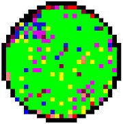
 The initial process supported by substrate maps was inkless binning.
Each tested die is assigned a bin value, depending on the result of the test. For example, a pass die is assigned a bin value of 1 for a good bin, bin 10 for an open circuit, and bin 11 for a short circuit. In the very early days of wafer test, the dies were put in different bins or buckets, depending on the test results.
Physical binning may no longer be used, but the analogy is still good. The next step in the process was to mark the failing dies with ink, so that during assembly only uninked dies were used for die attachment
and final assembly. The inking step may be skipped if the assembly equipment is able to access the information in the maps generated by the test equipment.
Where the substrate map applies to an entire wafer, the term 'wafer map' would be used, 'substrate map' is a more general term, applied to mapping in other areas of the semiconductors process: frames, trays and strips.
It supports many possible substrate maps, including the ones named above. While the old standards could only support standard bin maps, representing bin information, this standard also support transfermaps, which can help in tracing back dies on strips to the locations they come from of the wafer for example.
The concept also includes the package of data generated by modern wafer testing
Wafer testing
Wafer testing is a step performed during semiconductor device fabrication. During this step, performed before a wafer is sent to die preparation, all individual integrated circuits that are present on the wafer are tested for functional defects by applying special test patterns to them. The wafer...
equipment which can be transmitted to equipment used for subsequent 'back-end' manufacturing operations.
History
Each tested die is assigned a bin value, depending on the result of the test. For example, a pass die is assigned a bin value of 1 for a good bin, bin 10 for an open circuit, and bin 11 for a short circuit. In the very early days of wafer test, the dies were put in different bins or buckets, depending on the test results.
Physical binning may no longer be used, but the analogy is still good. The next step in the process was to mark the failing dies with ink, so that during assembly only uninked dies were used for die attachment
Die attachment
Die attachment is the step during the integrated circuit packaging phase of semiconductor device fabrication during which a die is mounted and fixed to the package or support structure....
and final assembly. The inking step may be skipped if the assembly equipment is able to access the information in the maps generated by the test equipment.
Where the substrate map applies to an entire wafer, the term 'wafer map' would be used, 'substrate map' is a more general term, applied to mapping in other areas of the semiconductors process: frames, trays and strips.
E142
As with many items in the Semiconductor process area, also for this process step there are standards available. The latest and most potential standard is the E142 standard, provided by the SEMI organization. This standard has been approved via ballots for release in 2005.It supports many possible substrate maps, including the ones named above. While the old standards could only support standard bin maps, representing bin information, this standard also support transfermaps, which can help in tracing back dies on strips to the locations they come from of the wafer for example.
External links
- SEMI organization: organization which is working on semiconductor process standards.