

Proximity effect (electron beam lithography)
Encyclopedia
The proximity effect in electron beam lithography
(EBL) is the phenomenon that the exposure dose distribution, and hence the developed pattern, is wider than the scanned pattern, due to the interactions of the primary beam electrons with the resist
and substrate. These cause the resist outside the scanned pattern to receive a non-zero dose.
Important contributions to weak resist polymer chain scission (for positive resists) or crosslinking (for negative resists) come from electron forward scattering and backscattering. The forward scattering process is due to electron-electron interactions which deflect the primary electrons by a typically small angle, thus statistically broadening the beam in the resist (and further in the substrate). The majority of the electrons do not stop in the resist but penetrate the substrate. These electrons can still contribute to resist exposure by scattering back into the resist and causing subsequent inelastic / exposing processes. This backscattering process originates e.g. from a collision with a heavy particle (i.e. substrate nucleus) and leads to wide angle scattering of the light electron from a range of depths (micrometres) in the substrate. The Rutherford backscattering probability increases quickly with substrate nuclear charge.
The above effects can be approximated by a simple two-gaussian model where a perfect point-like electron beam is broadened to a superposition of a gaussian with a width of a few nanometers to order 10's of nanometers, depending on the acceleration voltage, due to forward scattering and a gaussian with a width
  of the order of a few micrometers to order 10's due to backscattering, again depending on the acceleration voltage but also on the materials involved:
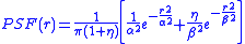
 is of order 1 so the contribution of backscattered electrons to the exposure is of the same order as the contribution of 'direct' forward scattered electrons.
  ,
,  and
and  are determined by the resist and substrate materials and the primary beam energy. The two-gaussian model parameters, including the development process, can be determined experimentally by exposing shapes for which the gaussian integral is easily solved, i.e. donuts, with increasing dose and observing at which dose the center resist clears / does not clear.
A thin resist with a low electron density will reduce forward scattering. A light substrate (light nuclei) will reduce backscattering. When electron beam lithography is performed on substrates with 'heavy' films, such as gold coatings, the backscatter effect will (depending on thickness) significantly increase. Increasing beam energy will reduce the forward scattering width, but since the beam penetrates the substrate more deeply, the backscatter width will increase.
The primary beam can transfer energy to electrons via elastic collisions with electrons and via inelastic collision processes such as impact ionization
. In the latter case, a secondary electron
is created and the energy state of the atom changes, which can result in the emission of Auger electrons or X-rays. The range of these secondary electrons is an energy-dependent accumulation of (inelastic) mean free paths; while not always a repeatable number, it is this range (up to 50 nm) that ultimately affects the practical resolution of the EBL process. The model described above can be extended for these effects.
Electron beam lithography
Electron beam lithography is the practice of emitting a beam of electrons in a patterned fashion across a surface covered with a film , and of selectively removing either exposed or non-exposed regions of the resist...
(EBL) is the phenomenon that the exposure dose distribution, and hence the developed pattern, is wider than the scanned pattern, due to the interactions of the primary beam electrons with the resist
Resist
In semiconductor fabrication, a resist is a thin layer used to transfer a circuit pattern to the semiconductor substrate which it is deposited upon. A resist can be patterned via lithography to form a micrometer-scale, temporary mask that protects selected areas of the underlying substrate during...
and substrate. These cause the resist outside the scanned pattern to receive a non-zero dose.
Important contributions to weak resist polymer chain scission (for positive resists) or crosslinking (for negative resists) come from electron forward scattering and backscattering. The forward scattering process is due to electron-electron interactions which deflect the primary electrons by a typically small angle, thus statistically broadening the beam in the resist (and further in the substrate). The majority of the electrons do not stop in the resist but penetrate the substrate. These electrons can still contribute to resist exposure by scattering back into the resist and causing subsequent inelastic / exposing processes. This backscattering process originates e.g. from a collision with a heavy particle (i.e. substrate nucleus) and leads to wide angle scattering of the light electron from a range of depths (micrometres) in the substrate. The Rutherford backscattering probability increases quickly with substrate nuclear charge.
The above effects can be approximated by a simple two-gaussian model where a perfect point-like electron beam is broadened to a superposition of a gaussian with a width
of a few nanometers to order 10's of nanometers, depending on the acceleration voltage, due to forward scattering and a gaussian with a width of the order of a few micrometers to order 10's due to backscattering, again depending on the acceleration voltage but also on the materials involved: is of order 1 so the contribution of backscattered electrons to the exposure is of the same order as the contribution of 'direct' forward scattered electrons. , and are determined by the resist and substrate materials and the primary beam energy. The two-gaussian model parameters, including the development process, can be determined experimentally by exposing shapes for which the gaussian integral is easily solved, i.e. donuts, with increasing dose and observing at which dose the center resist clears / does not clear.A thin resist with a low electron density will reduce forward scattering. A light substrate (light nuclei) will reduce backscattering. When electron beam lithography is performed on substrates with 'heavy' films, such as gold coatings, the backscatter effect will (depending on thickness) significantly increase. Increasing beam energy will reduce the forward scattering width, but since the beam penetrates the substrate more deeply, the backscatter width will increase.
The primary beam can transfer energy to electrons via elastic collisions with electrons and via inelastic collision processes such as impact ionization
Impact ionization
Impact ionization is the process in a material by which one energetic charge carrier can lose energy by the creation of other charge carriers...
. In the latter case, a secondary electron
Secondary electrons
Secondary electrons are electrons generated as ionization products. They are called 'secondary' because they are generated by other radiation . This radiation can be in the form of ions, electrons, or photons with sufficiently high energy, i.e. exceeding the ionization potential...
is created and the energy state of the atom changes, which can result in the emission of Auger electrons or X-rays. The range of these secondary electrons is an energy-dependent accumulation of (inelastic) mean free paths; while not always a repeatable number, it is this range (up to 50 nm) that ultimately affects the practical resolution of the EBL process. The model described above can be extended for these effects.