

X-ray lithography
Encyclopedia
X-ray
X-radiation is a form of electromagnetic radiation. X-rays have a wavelength in the range of 0.01 to 10 nanometers, corresponding to frequencies in the range 30 petahertz to 30 exahertz and energies in the range 120 eV to 120 keV. They are shorter in wavelength than UV rays and longer than gamma...
s to transfer a geometric pattern from a mask to a light-sensitive chemical photoresist
Photoresist
A photoresist is a light-sensitive material used in several industrial processes, such as photolithography and photoengraving to form a patterned coating on a surface.-Tone:Photoresists are classified into two groups: positive resists and negative resists....
, or simply "resist," on the substrate. A series of chemical treatments then engraves the produced pattern into the material underneath the photoresist.
Mechanisms
X-ray lithography originated as a candidate for next-generation lithographyNext-generation lithography
Next-generation lithography is a term used in integrated circuit manufacturing to describe the lithography technologies slated to replace photolithography. As of 2009 the most advanced form of photolithography is immersion lithography, in which water is used as an immersion medium for the final...
for the semiconductor
Semiconductor
A semiconductor is a material with electrical conductivity due to electron flow intermediate in magnitude between that of a conductor and an insulator. This means a conductivity roughly in the range of 103 to 10−8 siemens per centimeter...
industry, with batches of microprocessor
Microprocessor
A microprocessor incorporates the functions of a computer's central processing unit on a single integrated circuit, or at most a few integrated circuits. It is a multipurpose, programmable device that accepts digital data as input, processes it according to instructions stored in its memory, and...
s successfully produced. Having short wavelength
Wavelength
In physics, the wavelength of a sinusoidal wave is the spatial period of the wave—the distance over which the wave's shape repeats.It is usually determined by considering the distance between consecutive corresponding points of the same phase, such as crests, troughs, or zero crossings, and is a...
s (below 1 nm), X-rays overcome the diffraction
Diffraction
Diffraction refers to various phenomena which occur when a wave encounters an obstacle. Italian scientist Francesco Maria Grimaldi coined the word "diffraction" and was the first to record accurate observations of the phenomenon in 1665...
limits of optical lithography, allowing smaller feature sizes. If the X-ray source isn't collimated, as with a synchrotron radiation, elementary collimating mirrors or diffractive
Diffraction
Diffraction refers to various phenomena which occur when a wave encounters an obstacle. Italian scientist Francesco Maria Grimaldi coined the word "diffraction" and was the first to record accurate observations of the phenomenon in 1665...
lenses are used in the place of the refractive
Refraction
Refraction is the change in direction of a wave due to a change in its speed. It is essentially a surface phenomenon . The phenomenon is mainly in governance to the law of conservation of energy. The proper explanation would be that due to change of medium, the phase velocity of the wave is changed...
lenses used in optics. The X-rays illuminate a mask placed in proximity of a resist-coated wafer. The X-rays are broadband, typically from a compact synchrotron radiation
Synchrotron radiation
The electromagnetic radiation emitted when charged particles are accelerated radially is called synchrotron radiation. It is produced in synchrotrons using bending magnets, undulators and/or wigglers...
source, allowing rapid exposure. Deep X-ray lithography (DXRL) uses yet shorter wavelengths on the order of and modified procedures such as the LIGA
LIGA
LIGA is a German acronym for Lithographie, Galvanoformung, Abformung that describes a fabrication technology used to create high-aspect-ratio microstructures.-Overview:...
process, to fabricate deep and even three-dimensional structures.
The mask consists of an X-ray absorber, typically of gold
Gold
Gold is a chemical element with the symbol Au and an atomic number of 79. Gold is a dense, soft, shiny, malleable and ductile metal. Pure gold has a bright yellow color and luster traditionally considered attractive, which it maintains without oxidizing in air or water. Chemically, gold is a...
or compounds of tantalum
Tantalum
Tantalum is a chemical element with the symbol Ta and atomic number 73. Previously known as tantalium, the name comes from Tantalus, a character in Greek mythology. Tantalum is a rare, hard, blue-gray, lustrous transition metal that is highly corrosion resistant. It is part of the refractory...
or tungsten
Tungsten
Tungsten , also known as wolfram , is a chemical element with the chemical symbol W and atomic number 74.A hard, rare metal under standard conditions when uncombined, tungsten is found naturally on Earth only in chemical compounds. It was identified as a new element in 1781, and first isolated as...
, on a membrane that is transparent to X-rays, typically of silicon carbide
Silicon carbide
Silicon carbide , also known as carborundum, is a compound of silicon and carbon with chemical formula SiC. It occurs in nature as the extremely rare mineral moissanite. Silicon carbide powder has been mass-produced since 1893 for use as an abrasive...
or diamond
Diamond
In mineralogy, diamond is an allotrope of carbon, where the carbon atoms are arranged in a variation of the face-centered cubic crystal structure called a diamond lattice. Diamond is less stable than graphite, but the conversion rate from diamond to graphite is negligible at ambient conditions...
. The pattern on the mask is written by direct-write electron beam lithography
Electron beam lithography
Electron beam lithography is the practice of emitting a beam of electrons in a patterned fashion across a surface covered with a film , and of selectively removing either exposed or non-exposed regions of the resist...
onto a resist that is developed by conventional semiconductor processes. The membrane can be stretched for overlay accuracy.
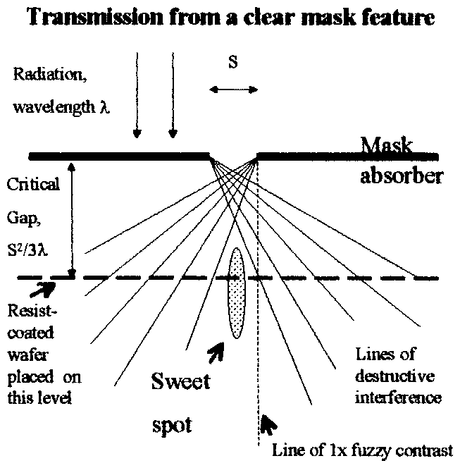
Most X-ray lithography demonstrations have been performed by copying with image fidelity (without magnification) on the line of fuzzy contrast as illustrated in the figure. However, with the increasing need for high resolution, X-ray lithography is now performed on what is called the "sweet spot", using local "demagnification by bias". Dense structures are developed by multiple exposures with translation. The advantages of using 3x demagnification include, the mask is more easily fabricated, the mask to wafer gap is increased, and the contrast is higher. The technique is extensible to dense prints.
X-rays generate secondary electrons as in the cases of extreme ultraviolet lithography
Extreme ultraviolet lithography
Extreme ultraviolet lithography is a next-generation lithography technology using an extreme ultraviolet wavelength, currently expected to be 13.5 nm.-EUVL light source:...
and electron beam lithography
Electron beam lithography
Electron beam lithography is the practice of emitting a beam of electrons in a patterned fashion across a surface covered with a film , and of selectively removing either exposed or non-exposed regions of the resist...
. While the fine pattern definition is due principally to secondaries from Auger electrons
Auger electron spectroscopy
Auger electron spectroscopy is a common analytical technique used specifically in the study of surfaces and, more generally, in the area of materials science...
with a short path length, the primary electrons will sensitize the resist over a larger region than the X-ray exposure. While this does not affect the pattern pitch resolution, which is determined by wavelength and gap, the image exposure contrast (max-min)/(max+min) is reduced because the pitch is on the order of the primary photo-electron range. The sidewall roughness and slopes are influenced by these secondary electrons as they can travel few micrometers in the area under the absorber, depending on exposure X-ray energy. Several prints at about have been published.
Another manifestation of the photoelectron effect is exposure to X-ray generated electrons from thick gold films used for making daughter masks. Simulations suggest that photoelectron generation from the gold substrate may affect dissolution rates.
Photoelectrons, secondary electrons and Auger electrons
Secondary electrons have energies of 25 eV or less, and can be generated by any ionizing radiation (VUVUltraviolet
Ultraviolet light is electromagnetic radiation with a wavelength shorter than that of visible light, but longer than X-rays, in the range 10 nm to 400 nm, and energies from 3 eV to 124 eV...
, EUV, X-rays, ions and other electrons). Auger electrons have energies of hundreds of electronvolts. The secondaries (generated by and outnumbering the Auger and primary photoelectrons) are the main agents for resist exposure.
The relative ranges of photoelectron primaries and Auger electrons depend on their respective energies. These energies depend on the energy of incident radiation and on the composition of the resist. There is considerable room for optimum selection (reference 3 of the article). When Auger electrons have lower energies than primary photoelectrons, they have shorter ranges. Both decay to secondaries which interact with chemical bonds. When secondary energies are too low, they fail to break the chemical bonds and cease to affect print resolution. Experiments prove that the combined range is less than 20 nm. On the other hand, the secondaries follow a different trend below ≈30 eV: the lower the energy, the longer the mean free path
Mean free path
In physics, the mean free path is the average distance covered by a moving particle between successive impacts which modify its direction or energy or other particle properties.-Derivation:...
though they are not then able to affect resist development.
As they decay, primary photo-electrons and Auger electrons eventually become physically indistinguishable (as in Fermi–Dirac statistics) from secondary electrons. The range of low-energy secondary electrons is sometimes larger than the range of primary photo-electrons or of Auger electrons. What matters for X-ray lithography is the effective range of electrons that have sufficient energy to make or break chemical bonds in negative or positive resists.
Lithographic electron range
X-rays do not charge. The relatively large mean free path (~20 nm) of secondary electrons hinders resolution control at nanometer scale. In particular, electron beam lithography suffers negative charging by incident electrons and consequent beam spread which limits resolution. It is difficult therefore to isolate the effective range of secondaries which may be less than 1 nm.The combined electron mean free path results in an image blur, which is usually modeled as a Gaussian function (where σ = blur) that is convolved with the expected image. As the desired resolution approaches the blur, the dose image becomes broader than the aerial image of the incident X-rays. The blur that matters is the latent image that describes the making or breaking of bonds during the exposure of resist. The developed image is the final relief image produced by the selected high contrast development process on the latent image.
The range of primary, Auger, secondary and ultralow energy higher-order generation electrons which print (as STM
Scanning tunneling microscope
A scanning tunneling microscope is an instrument for imaging surfaces at the atomic level. Its development in 1981 earned its inventors, Gerd Binnig and Heinrich Rohrer , the Nobel Prize in Physics in 1986. For an STM, good resolution is considered to be 0.1 nm lateral resolution and...
studies proved) can be large (tens of nm) or small (nm), according to various cited publications. Because this range is not a fixed number, it is hard to quantify. Line edge roughness is aggravated by the associated uncertainty. Line edge roughness is supposedly statistical in origin and only indirectly dependent on mean range. Under commonly practiced lithography conditions, the various electron ranges can be controlled and utilized.