

Theory of solar cell
Encyclopedia
The theory of solar cells explains the physical processes by which light is converted into electrical current when striking a suitable semiconductor device. The theoretical studies are of practical use because they predict the fundamental limits of solar cell performance, and give guidance on the phenomena that contribute to losses and solar cell efficiency
.
hits a piece of silicon, one of three things can happen:
When a photon is absorbed, its energy is given to an electron in the crystal lattice. Usually this electron is in the valence band
, and is tightly bound in covalent bonds between neighboring atoms, and hence unable to move far. The energy given to it by the photon "excites" it into the conduction band
, where it is free to move around within the semiconductor. The covalent bond that the electron was previously a part of now has one fewer electron — this is known as a hole. The presence of a missing covalent bond allows the bonded electrons of neighboring atoms to move into the "hole," leaving another hole behind, and in this way a hole can move through the lattice. Thus, it can be said that photons absorbed in the semiconductor create mobile electron-hole pairs.
A photon need only have greater energy than that of the band gap in order to excite an electron from the valence band into the conduction band. However, the solar frequency spectrum
approximates a black body
spectrum at about 5,800 K, and as such, much of the solar radiation reaching the Earth
is composed of photons with energies greater than the band gap of silicon. These higher energy photons will be absorbed by the solar cell, but the difference in energy between these photons and the silicon band gap is converted into heat (via lattice vibrations — called phonons) rather than into usable electrical energy.
In thick solar cells there is no electric field in the active region, so the dominant mode of charge carrier separation is diffusion. In these cells the diffusion length of minority carriers (the length that photo-generated carriers can travel before they recombine) must be large compared to the cell thickness. In thin film cells (such as amorphous silicon), the diffusion length of minority carriers is usually very short due to the existence of defects, and the dominant charge separation is therefore drift, driven by the electrostatic field of the junction, which extends to the whole thickness of the cell.
If a piece of p-type silicon is placed in intimate contact with a piece of n-type silicon, then a diffusion
of electrons occurs from the region of high electron concentration (the n-type side of the junction) into the region of low electron concentration (p-type side of the junction). When the electrons diffuse across the p-n junction, they recombine with holes on the p-type side. The diffusion of carriers does not happen indefinitely, however, because charges build up on either side of the junction and create an electric field
. The electric field creates a diode
that promotes charge flow, known as drift current
, that opposes and eventually balances out the diffusion of electrons and holes. This region where electrons and holes have diffused across the junction is called the depletion region because it no longer contains any mobile charge carriers. It is also known as the space charge region.
metal
-semiconductor contacts are made to both the n-type and p-type sides of the solar cell, and the electrodes connected to an external load. Electrons that are created on the n-type side, or have been "collected" by the junction and swept onto the n-type side, may travel through the wire, power the load, and continue through the wire until they reach the p-type semiconductor-metal contact. Here, they recombine with a hole that was either created as an electron-hole pair on the p-type side of the solar cell, or a hole that was swept across the junction from the n-type side after being created there.
The voltage measured is equal to the difference in the quasi Fermi levels of the minority carriers, i.e. electrons in the p-type portion and holes in the n-type portion.
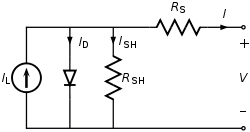

To understand the electronic behavior of a solar cell, it is useful to create a model
which is electrically equivalent, and is based on discrete electrical components whose behavior is well known. An ideal solar cell may be modelled by a current source in parallel with a diode
; in practice no solar cell is ideal, so a shunt
resistance and a series resistance component are added to the model. The resulting equivalent circuit of a solar cell is shown on the left. Also shown, on the right, is the schematic representation of a solar cell for use in circuit diagrams.

where
The current through these elements is governed by the voltage across them:

where
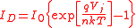
By the Shockley diode equation, the current diverted through the diode is:
where
By Ohm's law
, the current diverted through the shunt resistor is:

where
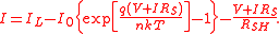
Substituting these into the first equation produces the characteristic equation of a solar cell, which relates solar cell parameters to the output current and voltage:
An alternative derivation produces an equation similar in appearance, but with V on the left-hand side. The two alternatives are identities
; that is, they yield precisely the same results.
In principle, given a particular operating voltage V the equation may be solved to determine the operating current I at that voltage. However, because the equation involves I on both sides in a transcendental function
the equation has no general analytical solution. However, even without a solution it is physically instructive. Furthermore, it is easily solved using numerical methods. (A general analytical solution to the equation is possible using Lambert's W function, but since Lambert's W generally itself must be solved numerically this is a technicality.)
Since the parameters I0, n, RS, and RSH cannot be measured directly, the most common application of the characteristic equation is nonlinear regression
to extract the values of these parameters on the basis of their combined effect on solar cell behavior.
Similarly, when the cell is operated at short circuit
, V = 0 and the current I through the terminals is defined as the short-circuit current. It can be shown that for a high-quality solar cell (low RS and I0, and high RSH) the short-circuit current ISC is:

It should be noted that it is not possible to extract any power from the device when operating at either open circuit or short circuit conditions.
, or current produced per unit cell area:
where
This formulation has several advantages. One is that since cell characteristics are referenced to a common cross-sectional area they may be compared for cells of different physical dimensions. While this is of limited benefit in a manufacturing setting, where all cells tend to be the same size, it is useful in research and in comparing cells between manufacturers. Another advantage is that the density equation naturally scales the parameter values to similar orders of magnitude, which can make numerical extraction of them simpler and more accurate even with naive solution methods.
There are practical limitations of this formulation. For instance, certain parasitic effects grow in importance as cell sizes shrink and can affect the extracted parameter values. Recombination and contamination of the junction tend to be greatest at the perimeter of the cell, so very small cells may exhibit higher values of J0 or lower values of RSH than larger cells that are otherwise identical. In such cases, comparisons between cells must be made cautiously and with these effects in mind.
This approach should only be used for comparing solar cells with comparable layout. For instance, a comparison between primarily quadratical solar cells like typical crystalline silicon solar cells and narrow but long solar cells like typical thin film solar cell
s can lead to wrong assumptions caused by the different kinds of current paths and therefore the influence of for instance a distributed series resistance rS.
 Temperature affects the characteristic equation in two ways: directly, via T in the exponential term, and indirectly via its effect on I0 (strictly speaking, temperature affects all of the terms, but these two far more significantly than the others). While increasing T reduces the magnitude of the exponent in the characteristic equation, the value of I0 increases exponentially with T. The net effect is to reduce VOC (the open-circuit voltage) linearly with increasing temperature. The magnitude of this reduction is inversely proportional to VOC; that is, cells with higher values of VOC suffer smaller reductions in voltage with increasing temperature. For most crystalline silicon solar cells the change in VOC with temperature is about -0.50%/°C, though the rate for the highest-efficiency crystalline silicon cells is around -0.35%/°C. By way of comparison, the rate for amorphous silicon solar cells is -0.20%/°C to -0.30%/°C, depending on how the cell is made.
The amount of photogenerated current IL increases slightly with increasing temperature because of an increase in the number of thermally generated carriers in the cell. This effect is slight, however: about 0.065%/°C for crystalline silicon cells and 0.09% for amorphous silicon cells.
The overall effect of temperature on cell efficiency can be computed using these factors in combination with the characteristic equation. However, since the change in voltage is much stronger than the change in current, the overall effect on efficiency tends to be similar to that on voltage. Most crystalline silicon solar cells decline in efficiency by 0.50%/°C and most amorphous cells decline by 0.15-0.25%/°C. The figure above shows I-V curves that might typically be seen for a crystalline silicon solar cell at various temperatures.
 As series resistance increases, the voltage drop between the junction voltage and the terminal voltage becomes greater for the same current. The result is that the current-controlled portion of the I-V curve begins to sag toward the origin, producing a significant decrease in the terminal voltage
  and a slight reduction in ISC, the short-circuit current. Very high values of RS will also produce a significant reduction in ISC; in these regimes, series resistance dominates and the behavior of the solar cell resembles that of a resistor. These effects are shown for crystalline silicon solar cells in the I-V curves displayed in the figure to the right.
Losses caused by series resistance are in a first approximation given by Ploss=VRsI=I2RS and increase quadratically with (photo-)current. Series resistance losses are therefore most important at high illumination intensities.
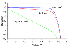 As shunt resistance decreases, the current diverted through the shunt resistor increases for a given level of junction voltage. The result is that the voltage-controlled portion of the I-V curve begins to sag toward the origin, producing a significant decrease in the terminal current I and a slight reduction in VOC. Very low values of RSH will produce a significant reduction in VOC. Much as in the case of a high series resistance, a badly shunted solar cell will take on operating characteristics similar to those of a resistor. These effects are shown for crystalline silicon solar cells in the I-V curves displayed in the figure to the right.
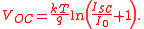
 If one assumes infinite shunt resistance, the characteristic equation can be solved for VOC:
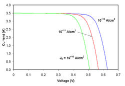
Thus, an increase in I0 produces a reduction in VOC proportional to the inverse of the logarithm of the increase. This explains mathematically the reason for the reduction in VOC that accompanies increases in temperature described above. The effect of reverse saturation current on the I-V curve of a crystalline silicon solar cell are shown in the figure to the right. Physically, reverse saturation current is a measure of the "leakage" of carriers across the p-n junction in reverse bias. This leakage is a result of carrier recombination in the neutral regions on either side of the junction.
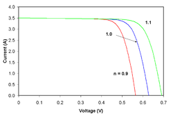 The ideality factor (also called the emissivity factor) is a fitting parameter that describes how closely the diode's behavior matches that predicted by theory, which assumes the p-n junction of the diode is an infinite plane and no recombination occurs within the space-charge region. A perfect match to theory is indicated when n = 1. When recombination in the space-charge region dominate other recombination, however, n = 2. The effect of changing ideality factor independently of all other parameters is shown for a crystalline silicon solar cell in the I-V curves displayed in the figure to the right.
Most solar cells, which are quite large compared to conventional diodes, well approximate an infinite plane and will usually exhibit near-ideal behavior under Standard Test Condition (n ≈ 1). Under certain operating conditions, however, device operation may be dominated by recombination in the space-charge region. This is characterized by a significant increase in I0 as well as an increase in ideality factor to n ≈ 2. The latter tends to increase solar cell output voltage while the former acts to erode it. The net effect, therefore, is a combination of the increase in voltage shown for increasing n in the figure to the right and the decrease in voltage shown for increasing I0 in the figure above. Typically, I0 is the more significant factor and the result is a reduction in voltage.
Solar cell efficiency
The efficiency of a solar cell may be broken down into reflectance efficiency, thermodynamic efficiency, charge carrier separation efficiency and conductive efficiency...
.
Simple explanation
- PhotonPhotonIn physics, a photon is an elementary particle, the quantum of the electromagnetic interaction and the basic unit of light and all other forms of electromagnetic radiation. It is also the force carrier for the electromagnetic force...
s in sunlightSunlightSunlight, in the broad sense, is the total frequency spectrum of electromagnetic radiation given off by the Sun. On Earth, sunlight is filtered through the Earth's atmosphere, and solar radiation is obvious as daylight when the Sun is above the horizon.When the direct solar radiation is not blocked...
hit the solar panel and are absorbed by semiconducting materials, such as silicon. - Electrons (negatively charged) are knocked loose from their atoms, allowing them to flow through the material to produce electricity. Due to the special composition of solar cells, the electrons are only allowed to move in a single direction.
- An array of solar cells converts solar energy into a usable amount of direct currentDirect currentDirect current is the unidirectional flow of electric charge. Direct current is produced by such sources as batteries, thermocouples, solar cells, and commutator-type electric machines of the dynamo type. Direct current may flow in a conductor such as a wire, but can also flow through...
(DC) electricity.
Photogeneration of charge carriers
When a photonPhoton
In physics, a photon is an elementary particle, the quantum of the electromagnetic interaction and the basic unit of light and all other forms of electromagnetic radiation. It is also the force carrier for the electromagnetic force...
hits a piece of silicon, one of three things can happen:
- the photon can pass straight through the silicon — this (generally) happens for lower energy photons,
- the photon can reflect off the surface,
- the photon can be absorbed by the silicon, if the photon energy is higher than the silicon band gapBand gapIn solid state physics, a band gap, also called an energy gap or bandgap, is an energy range in a solid where no electron states can exist. In graphs of the electronic band structure of solids, the band gap generally refers to the energy difference between the top of the valence band and the...
value. This generates an electron-hole pair and sometimes heat, depending on the band structure.
When a photon is absorbed, its energy is given to an electron in the crystal lattice. Usually this electron is in the valence band
Valence band
In solids, the valence band is the highest range of electron energies in which electrons are normally present at absolute zero temperature....
, and is tightly bound in covalent bonds between neighboring atoms, and hence unable to move far. The energy given to it by the photon "excites" it into the conduction band
Conduction band
In the solid-state physics field of semiconductors and insulators, the conduction band is the range of electron energies, higher than that of the valence band, sufficient to free an electron from binding with its individual atom and allow it to move freely within the atomic lattice of the material...
, where it is free to move around within the semiconductor. The covalent bond that the electron was previously a part of now has one fewer electron — this is known as a hole. The presence of a missing covalent bond allows the bonded electrons of neighboring atoms to move into the "hole," leaving another hole behind, and in this way a hole can move through the lattice. Thus, it can be said that photons absorbed in the semiconductor create mobile electron-hole pairs.
A photon need only have greater energy than that of the band gap in order to excite an electron from the valence band into the conduction band. However, the solar frequency spectrum
Frequency spectrum
The frequency spectrum of a time-domain signal is a representation of that signal in the frequency domain. The frequency spectrum can be generated via a Fourier transform of the signal, and the resulting values are usually presented as amplitude and phase, both plotted versus frequency.Any signal...
approximates a black body
Black body
A black body is an idealized physical body that absorbs all incident electromagnetic radiation. Because of this perfect absorptivity at all wavelengths, a black body is also the best possible emitter of thermal radiation, which it radiates incandescently in a characteristic, continuous spectrum...
spectrum at about 5,800 K, and as such, much of the solar radiation reaching the Earth
Earth
Earth is the third planet from the Sun, and the densest and fifth-largest of the eight planets in the Solar System. It is also the largest of the Solar System's four terrestrial planets...
is composed of photons with energies greater than the band gap of silicon. These higher energy photons will be absorbed by the solar cell, but the difference in energy between these photons and the silicon band gap is converted into heat (via lattice vibrations — called phonons) rather than into usable electrical energy.
Charge carrier separation
There are two main modes for charge carrier separation in a solar cell:- drift of carriers, driven by an electric field established across the device
- diffusion of carriers due to their random thermal motion, until they are captured by the electrical fields existing at the edges of the active region.
In thick solar cells there is no electric field in the active region, so the dominant mode of charge carrier separation is diffusion. In these cells the diffusion length of minority carriers (the length that photo-generated carriers can travel before they recombine) must be large compared to the cell thickness. In thin film cells (such as amorphous silicon), the diffusion length of minority carriers is usually very short due to the existence of defects, and the dominant charge separation is therefore drift, driven by the electrostatic field of the junction, which extends to the whole thickness of the cell.
The p-n junction
The most commonly known solar cell is configured as a large-area p-n junction made from silicon. As a simplification, one can imagine bringing a layer of n-type silicon into direct contact with a layer of p-type silicon. In practice, p-n junctions of silicon solar cells are not made in this way, but rather by diffusing an n-type dopant into one side of a p-type wafer (or vice versa).If a piece of p-type silicon is placed in intimate contact with a piece of n-type silicon, then a diffusion
Diffusion
Molecular diffusion, often called simply diffusion, is the thermal motion of all particles at temperatures above absolute zero. The rate of this movement is a function of temperature, viscosity of the fluid and the size of the particles...
of electrons occurs from the region of high electron concentration (the n-type side of the junction) into the region of low electron concentration (p-type side of the junction). When the electrons diffuse across the p-n junction, they recombine with holes on the p-type side. The diffusion of carriers does not happen indefinitely, however, because charges build up on either side of the junction and create an electric field
Electric field
In physics, an electric field surrounds electrically charged particles and time-varying magnetic fields. The electric field depicts the force exerted on other electrically charged objects by the electrically charged particle the field is surrounding...
. The electric field creates a diode
Diode
In electronics, a diode is a type of two-terminal electronic component with a nonlinear current–voltage characteristic. A semiconductor diode, the most common type today, is a crystalline piece of semiconductor material connected to two electrical terminals...
that promotes charge flow, known as drift current
Drift current
In condensed matter physics and electrochemistry, drift current is the electric current, or movement of charge carriers, which is due to the applied electric field, often stated as the electromotive force over a given distance.When an electric field is applied across a semiconductor material,the...
, that opposes and eventually balances out the diffusion of electrons and holes. This region where electrons and holes have diffused across the junction is called the depletion region because it no longer contains any mobile charge carriers. It is also known as the space charge region.
Connection to an external load
OhmicOhmic contact
An ohmic contact is a region on a semiconductor device that has been prepared so that the current-voltage curve of the device is linear and symmetric. If the I-V characteristic is non-linear and asymmetric, the contact is not ohmic, but is a blocking or Schottky contact...
metal
Metal
A metal , is an element, compound, or alloy that is a good conductor of both electricity and heat. Metals are usually malleable and shiny, that is they reflect most of incident light...
-semiconductor contacts are made to both the n-type and p-type sides of the solar cell, and the electrodes connected to an external load. Electrons that are created on the n-type side, or have been "collected" by the junction and swept onto the n-type side, may travel through the wire, power the load, and continue through the wire until they reach the p-type semiconductor-metal contact. Here, they recombine with a hole that was either created as an electron-hole pair on the p-type side of the solar cell, or a hole that was swept across the junction from the n-type side after being created there.
The voltage measured is equal to the difference in the quasi Fermi levels of the minority carriers, i.e. electrons in the p-type portion and holes in the n-type portion.
Equivalent circuit of a solar cell
To understand the electronic behavior of a solar cell, it is useful to create a model
Model (physical)
A physical model is a smaller or larger physical copy of an object...
which is electrically equivalent, and is based on discrete electrical components whose behavior is well known. An ideal solar cell may be modelled by a current source in parallel with a diode
Diode
In electronics, a diode is a type of two-terminal electronic component with a nonlinear current–voltage characteristic. A semiconductor diode, the most common type today, is a crystalline piece of semiconductor material connected to two electrical terminals...
; in practice no solar cell is ideal, so a shunt
Shunt (electrical)
In electronics, a shunt is a device which allows electric current to pass around another point in the circuit. The term is also widely used in photovoltaics to describe an unwanted short circuit between the front and back surface contacts of a solar cell, usually caused by wafer damage.-Defective...
resistance and a series resistance component are added to the model. The resulting equivalent circuit of a solar cell is shown on the left. Also shown, on the right, is the schematic representation of a solar cell for use in circuit diagrams.
Characteristic equation
From the equivalent circuit it is evident that the current produced by the solar cell is equal to that produced by the current source, minus that which flows through the diode, minus that which flows through the shunt resistor:where
- I = output current (amperes)
- IL = photogenerated current (amperes)
- ID = diode current (amperes)
- ISH = shunt current (amperes).
The current through these elements is governed by the voltage across them:
where
- Vj = voltage across both diode and resistor RSH (volts)
- V = voltage across the output terminals (volts)
- I = output current (amperes)
- RS = series resistance (Ω).
By the Shockley diode equation, the current diverted through the diode is:
where
- I0 = reverse saturation currentSaturation currentSaturation current is a term used in relation to semiconductor diodes. It is more fully, and accurately, named reverse saturation current and is "part of the reverse current in a diode caused by diffusion of minority carriers from the neutral regions to the depletion region...
(amperes) - n = diode ideality factor (1 for an ideal diode)
- q = elementary chargeElementary chargeThe elementary charge, usually denoted as e, is the electric charge carried by a single proton, or equivalently, the absolute value of the electric charge carried by a single electron. This elementary charge is a fundamental physical constant. To avoid confusion over its sign, e is sometimes called...
- k = Boltzmann's constant
- T = absolute temperature
- At 25°C,
 volts.
By Ohm's law
Ohm's law
Ohm's law states that the current through a conductor between two points is directly proportional to the potential difference across the two points...
, the current diverted through the shunt resistor is:
where
- RSH = shunt resistance (Ω).
Substituting these into the first equation produces the characteristic equation of a solar cell, which relates solar cell parameters to the output current and voltage:
An alternative derivation produces an equation similar in appearance, but with V on the left-hand side. The two alternatives are identities
Identity (mathematics)
In mathematics, the term identity has several different important meanings:*An identity is a relation which is tautologically true. This means that whatever the number or value may be, the answer stays the same. For example, algebraically, this occurs if an equation is satisfied for all values of...
; that is, they yield precisely the same results.
In principle, given a particular operating voltage V the equation may be solved to determine the operating current I at that voltage. However, because the equation involves I on both sides in a transcendental function
Transcendental function
A transcendental function is a function that does not satisfy a polynomial equation whose coefficients are themselves polynomials, in contrast to an algebraic function, which does satisfy such an equation...
the equation has no general analytical solution. However, even without a solution it is physically instructive. Furthermore, it is easily solved using numerical methods. (A general analytical solution to the equation is possible using Lambert's W function, but since Lambert's W generally itself must be solved numerically this is a technicality.)
Since the parameters I0, n, RS, and RSH cannot be measured directly, the most common application of the characteristic equation is nonlinear regression
Nonlinear regression
In statistics, nonlinear regression is a form of regression analysis in which observational data are modeled by a function which is a nonlinear combination of the model parameters and depends on one or more independent variables...
to extract the values of these parameters on the basis of their combined effect on solar cell behavior.
Open-circuit voltage and short-circuit current
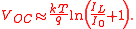
When the cell is operated at open circuit, I = 0 and the voltage across the output terminals is defined as the open-circuit voltage. Assuming the shunt resistance is high enough to neglect the final term of the characteristic equation, the open-circuit voltage VOC is:Similarly, when the cell is operated at short circuit
Short circuit
A short circuit in an electrical circuit that allows a current to travel along an unintended path, often where essentially no electrical impedance is encountered....
, V = 0 and the current I through the terminals is defined as the short-circuit current. It can be shown that for a high-quality solar cell (low RS and I0, and high RSH) the short-circuit current ISC is:
It should be noted that it is not possible to extract any power from the device when operating at either open circuit or short circuit conditions.
Effect of physical size
The values of I0, RS, and RSH are dependent upon the physical size of the solar cell. In comparing otherwise identical cells, a cell with twice the surface area of another will, in principle, have double the I0 because it has twice the junction area across which current can leak. It will also have half the RS and RSH because it has twice the cross-sectional area through which current can flow. For this reason, the characteristic equation is frequently written in terms of current densityCurrent density
Current density is a measure of the density of flow of a conserved charge. Usually the charge is the electric charge, in which case the associated current density is the electric current per unit area of cross section, but the term current density can also be applied to other conserved...
, or current produced per unit cell area:
where
- J = current density (amperes/cm2)
- JL = photogenerated current density (amperes/cm2)
- J0 = reverse saturation current density (amperes/cm2)
- rS = specific series resistance (Ω-cm2)
- rSH = specific shunt resistance (Ω-cm2).
This formulation has several advantages. One is that since cell characteristics are referenced to a common cross-sectional area they may be compared for cells of different physical dimensions. While this is of limited benefit in a manufacturing setting, where all cells tend to be the same size, it is useful in research and in comparing cells between manufacturers. Another advantage is that the density equation naturally scales the parameter values to similar orders of magnitude, which can make numerical extraction of them simpler and more accurate even with naive solution methods.
There are practical limitations of this formulation. For instance, certain parasitic effects grow in importance as cell sizes shrink and can affect the extracted parameter values. Recombination and contamination of the junction tend to be greatest at the perimeter of the cell, so very small cells may exhibit higher values of J0 or lower values of RSH than larger cells that are otherwise identical. In such cases, comparisons between cells must be made cautiously and with these effects in mind.
This approach should only be used for comparing solar cells with comparable layout. For instance, a comparison between primarily quadratical solar cells like typical crystalline silicon solar cells and narrow but long solar cells like typical thin film solar cell
Thin film solar cell
A thin-film solar cell , also called a thin-film photovoltaic cell , is a solar cell that is made by depositing one or more thin layers of photovoltaic material on a substrate...
s can lead to wrong assumptions caused by the different kinds of current paths and therefore the influence of for instance a distributed series resistance rS.
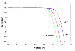
Cell temperature
The amount of photogenerated current IL increases slightly with increasing temperature because of an increase in the number of thermally generated carriers in the cell. This effect is slight, however: about 0.065%/°C for crystalline silicon cells and 0.09% for amorphous silicon cells.
The overall effect of temperature on cell efficiency can be computed using these factors in combination with the characteristic equation. However, since the change in voltage is much stronger than the change in current, the overall effect on efficiency tends to be similar to that on voltage. Most crystalline silicon solar cells decline in efficiency by 0.50%/°C and most amorphous cells decline by 0.15-0.25%/°C. The figure above shows I-V curves that might typically be seen for a crystalline silicon solar cell at various temperatures.
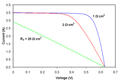
Series resistance
and a slight reduction in ISC, the short-circuit current. Very high values of RS will also produce a significant reduction in ISC; in these regimes, series resistance dominates and the behavior of the solar cell resembles that of a resistor. These effects are shown for crystalline silicon solar cells in the I-V curves displayed in the figure to the right.Losses caused by series resistance are in a first approximation given by Ploss=VRsI=I2RS and increase quadratically with (photo-)current. Series resistance losses are therefore most important at high illumination intensities.
Shunt resistance
Reverse saturation current
Thus, an increase in I0 produces a reduction in VOC proportional to the inverse of the logarithm of the increase. This explains mathematically the reason for the reduction in VOC that accompanies increases in temperature described above. The effect of reverse saturation current on the I-V curve of a crystalline silicon solar cell are shown in the figure to the right. Physically, reverse saturation current is a measure of the "leakage" of carriers across the p-n junction in reverse bias. This leakage is a result of carrier recombination in the neutral regions on either side of the junction.
Ideality factor
Most solar cells, which are quite large compared to conventional diodes, well approximate an infinite plane and will usually exhibit near-ideal behavior under Standard Test Condition (n ≈ 1). Under certain operating conditions, however, device operation may be dominated by recombination in the space-charge region. This is characterized by a significant increase in I0 as well as an increase in ideality factor to n ≈ 2. The latter tends to increase solar cell output voltage while the former acts to erode it. The net effect, therefore, is a combination of the increase in voltage shown for increasing n in the figure to the right and the decrease in voltage shown for increasing I0 in the figure above. Typically, I0 is the more significant factor and the result is a reduction in voltage.