
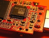
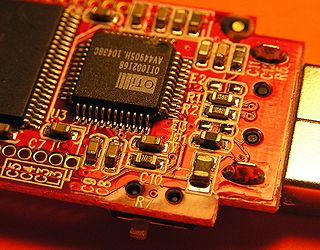
Surface-mount technology
Encyclopedia
Electronics
Electronics is the branch of science, engineering and technology that deals with electrical circuits involving active electrical components such as vacuum tubes, transistors, diodes and integrated circuits, and associated passive interconnection technologies...
circuits in which the components (surface-mounted components/SMCs) are mounted directly onto the surface of printed circuit board
Printed circuit board
A printed circuit board, or PCB, is used to mechanically support and electrically connect electronic components using conductive pathways, tracks or signal traces etched from copper sheets laminated onto a non-conductive substrate. It is also referred to as printed wiring board or etched wiring...
s (PCBs). An electronic device so made is called a surface mount device (SMD). In the industry it has largely replaced the through-hole technology
Through-hole technology
Through-hole technology, also spelled "thru-hole", refers to the mounting scheme used for electronic components that involves the use of leads on the components that are inserted into holes drilled in printed circuit boards and soldered to pads on the opposite side either by manual assembly by...
construction method of fitting components with wire leads into holes in the circuit board.
An SMT component is usually smaller than its through-hole counterpart because it has either smaller leads or no leads at all. It may have short pin
Lead (electronics)
In electronics, a lead is an electrical connection consisting of a length of wire or soldering pad that comes from a device. Leads are used for physical support, to transfer power, to probe circuits , and to transmit information...
s or leads of various styles, flat contacts, a matrix of solder balls (BGA
Ball grid array
A ball grid array is a type of surface-mount packaging used for integrated circuits.- Description :The BGA is descended from the pin grid array , which is a package with one face covered with pins in a grid pattern. These pins conduct electrical signals from the integrated circuit to the printed...
s), or terminations on the body of the component.
History
Surface mount technology was developed in the 1960s and became widely used in the late 1980s. Much of the pioneering work in this technology was by IBMIBM
International Business Machines Corporation or IBM is an American multinational technology and consulting corporation headquartered in Armonk, New York, United States. IBM manufactures and sells computer hardware and software, and it offers infrastructure, hosting and consulting services in areas...
. The design approach first demonstrated by IBM in 1960 in the a small-scale computer was later applied in the Launch Vehicle Digital Computer used in the Instrument Unit
Saturn V Instrument Unit
The Saturn V Instrument Unit is a ring-shaped structure fitted to the top of the Saturn V rocket's third stage and the Saturn IB's second stage . It was immediately below the SLA panels that contained the Lunar Module. The Instrument Unit contains the guidance system for the Saturn V rocket...
that guided all Saturn IB
Saturn IB
The Saturn IB was an American launch vehicle commissioned by the National Aeronautics and Space Administration for use in the Apollo program...
and Saturn V
Saturn V
The Saturn V was an American human-rated expendable rocket used by NASA's Apollo and Skylab programs from 1967 until 1973. A multistage liquid-fueled launch vehicle, NASA launched 13 Saturn Vs from the Kennedy Space Center, Florida with no loss of crew or payload...
vehicles. Components were mechanically redesigned to have small metal tabs or end caps that could be directly soldered to the surface of the PCB. Components became much smaller and component placement on both sides of a board became far more common with surface mounting than through-hole mounting, allowing much higher circuit densities. Often only the solder joints hold the parts to the board, although parts on the bottom or "second" side of the board are temporarily secured with a dot of adhesive as well. Surface mounted devices (SMDs) are usually made physically small and lightweight for this reason. Surface mounting lends itself well to a high degree of automation, reducing labor cost and greatly increasing production rates. SMDs can be one-quarter to one-tenth the size and weight, and one-half to one-quarter the cost of equivalent through-hole parts.
Terms
| SMp DIALECT | Expanded Form |
|---|---|
| SMD | Surface Mount Devices (active, passive and electromechanical components) |
| SMT | Surface Mount Technology (assembling and montage technology) |
| SMA | Surface Mount Assembly (module assembled with SMT) |
| SMC | Surface Mount Components (components for SMT) |
| SMP | Surface Mount Packages (SMD case forms) |
| SME | Surface Mount Equipment (SMT assembling machines) |
| SO | Small Outline (4 to 28 pins) |
| VSO | Very Small Outline (40 pins) |
| SOP | Small Outline Package (case) |
| SOD | Small Outline Diode |
| SOT | Small Outline Transistor |
| SOIC | Small Outline Integrated Circuit |
| CC | Chip Carrier |
| LCC | Leadless Chip Carrier |
| PLCC | Plastic Leaded Chip Carrier |
| LCCC | Leadless Ceramic Chip Carrier |
| MELF | Metal Electrode Face Bonding |
| MINI MELF | Mini Metal Electrode Face Bonding |
| MICRO MELF | Micro Metal Electrode Face Bonding |
Assembly techniques
Tin
Tin is a chemical element with the symbol Sn and atomic number 50. It is a main group metal in group 14 of the periodic table. Tin shows chemical similarity to both neighboring group 14 elements, germanium and lead and has two possible oxidation states, +2 and the slightly more stable +4...
-lead, silver, or gold plated copper
Copper
Copper is a chemical element with the symbol Cu and atomic number 29. It is a ductile metal with very high thermal and electrical conductivity. Pure copper is soft and malleable; an exposed surface has a reddish-orange tarnish...
pads without holes, called solder pads. Solder paste
Solder paste
Solder paste sometimes refers to soldering flux that does not contain solder.Solder paste is used to connect the leads of integrated chip packages to attachment points in the circuit patterns on a printed circuit board...
, a sticky mixture of flux
Flux (metallurgy)
In metallurgy, a flux , is a chemical cleaning agent, flowing agent, or purifying agent. Fluxes may have more than one function at a time...
and tiny solder particles, is first applied to all the solder pads with a stainless steel or nickel stencil using a screen printing process. It can also be applied by a jet-printing mechanism, similar to an inkjet printer
Inkjet printer
An inkjet printer is a type of computer printer that creates a digital image by propelling droplets of ink onto paper. Inkjet printers are the most commonly used type of printer and range from small inexpensive consumer models to very large professional machines that can cost up to thousands of...
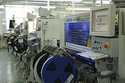
. After pasting, the boards then proceed to the pick-and-place machines
SMT Placement Equipment
SMT component placement systems, commonly called pick-and-place machines or P&Ps, are robotic machines which are used to place surface-mount devices onto a printed circuit board...
, where they are placed on a conveyor belt. The components to be placed on the boards are usually delivered to the production line in either paper/plastic tapes wound on reels or plastic tubes. Some large integrated circuits are delivered in static-free trays. Numerical control
Numerical control
Numerical control refers to the automation of machine tools that are operated by abstractly programmed commands encoded on a storage medium, as opposed to controlled manually via handwheels or levers, or mechanically automated via cams alone...
pick-and-place machines remove the parts from the tapes, tubes or trays and place them on the PCB.
The boards are then conveyed into the reflow soldering
Reflow soldering
Reflow soldering is a process in which a solder paste is used to temporarily attach one or several electrical components to their contact pads, after which the entire assembly is subjected to controlled heat, which melts the solder, permanently connecting the joint...
oven. They first enter a pre-heat zone, where the temperature of the board and all the components is gradually, uniformly raised. The boards then enter a zone where the temperature is high enough to melt the solder particles in the solder paste, bonding the component leads to the pads on the circuit board. The surface tension of the molten solder helps keep the components in place, and if the solder pad geometries are correctly designed, surface tension
Surface tension
Surface tension is a property of the surface of a liquid that allows it to resist an external force. It is revealed, for example, in floating of some objects on the surface of water, even though they are denser than water, and in the ability of some insects to run on the water surface...
automatically aligns the components on their pads. There are a number of techniques for reflowing solder. One is to use infrared
Infrared
Infrared light is electromagnetic radiation with a wavelength longer than that of visible light, measured from the nominal edge of visible red light at 0.74 micrometres , and extending conventionally to 300 µm...
lamps; this is called infrared reflow. Another is to use a hot gas convection
Convection
Convection is the movement of molecules within fluids and rheids. It cannot take place in solids, since neither bulk current flows nor significant diffusion can take place in solids....
. Another technology which is becoming popular again is special fluorocarbon
Fluorocarbon
Fluorocarbons, sometimes referred to as perfluorocarbons or PFCs, are organofluorine compounds that contain only carbon and fluorine bonded together in strong carbon–fluorine bonds. Fluoroalkanes that contain only single bonds are more chemically and thermally stable than alkanes...
liquids with high boiling points which use a method called vapor phase reflow. Due to environmental concerns, this method was falling out of favor until lead-free legislation was introduced which requires tighter controls on soldering. Currently, at the end of 2008, convection soldering is the most popular reflow technology using either standard air or nitrogen gas. Each method has its advantages and disadvantages. With infrared reflow, the board designer must lay the board out so that short components don't fall into the shadows of tall components. Component location is less restricted if the designer knows that vapor phase reflow or convection soldering will be used in production. Following reflow soldering, certain irregular or heat-sensitive components may be installed and soldered by hand, or in large scale automation, by focused infrared beam (FIB) or localized convection equipment.
If the circuit board is double sided then this printing, placement, reflow process may be repeated using either solder paste or glue to hold the components in place. If glue
Glue
This is a list of various types of glue. Historically, the term "glue" only referred to protein colloids prepared from animal flesh. The meaning has been extended to refer to any fluid adhesive....
is used then the parts must be soldered later using a wave soldering
Wave soldering
Wave soldering is a large-scale soldering process by which electronic components are soldered to a printed circuit board to form an electronic assembly. The name is derived from the use of waves of molten solder to attach metal components to the PCB...
process.
After soldering, the boards may be washed to remove flux residues and any stray solder balls that could short out closely spaced component leads. Rosin
Rosin
.Rosin, also called colophony or Greek pitch , is a solid form of resin obtained from pines and some other plants, mostly conifers, produced by heating fresh liquid resin to vaporize the volatile liquid terpene components. It is semi-transparent and varies in color from yellow to black...
flux is removed with fluorocarbon solvents, high flash point
Flash point
The flash point of a volatile material is the lowest temperature at which it can vaporize to form an ignitable mixture in air. Measuring a flash point requires an ignition source...
hydrocarbon
Hydrocarbon
In organic chemistry, a hydrocarbon is an organic compound consisting entirely of hydrogen and carbon. Hydrocarbons from which one hydrogen atom has been removed are functional groups, called hydrocarbyls....
solvents, or low flash solvents e.g. limonene
Limonene
Limonene is a colourless liquid hydrocarbon classified as a cyclic terpene. The more common D isomer possesses a strong smell of oranges. It is used in chemical synthesis as a precursor to carvone and as a renewably-based solvent in cleaning products....
(derived from orange peels) which require extra rinsing or drying cycles. Water soluble fluxes are removed with deionized water and detergent, followed by an air blast to quickly remove residual water. However, most electronic assemblies are made using a "No-Clean" process where the flux residues are designed to be left on the circuit board [Benign]. This saves the cost of cleaning, speeds up the manufacturing process, and reduces waste.
Finally, the boards are visually inspected for missing or misaligned components and solder bridging. If needed, they are sent to a rework station where a human operator repairs any errors. They are then usually sent to the testing stations (in-circuit testing and/or functional testing) to verify that they operate correctly.
Advantages
The main advantages of SMT over the older through-hole technique are:- Smaller components. Smallest is currently 0.2 x 0.1 mm (0.01 in x 0.005 in: 01005).
- Much higher number of components and many more connections per component.
- Fewer holes need to be drilled through abrasive boards.
- Simpler automated assembly.
- Small errors in component placement are corrected automatically (the surface tension of the molten solder pulls the component into alignment with the solder pads).
- Components can be placed on both sides of the circuit board.
- Lower resistance and inductance at the connection (leading to better performance for high frequency parts).
- Better mechanical performance under shake and vibration conditions.
- SMT parts generally cost less than through-hole parts.
- Fewer unwanted RF signal effects in SMT parts when compared to leaded parts, yielding better predictability of component characteristics.
- Faster assembly. Some placement machines are capable of placing more than 136,000 components per hour.
Disadvantages
- The manufacturing processes for SMT are much more sophisticated than through-hole boards, raising the initial cost and time of setting up for production.
- Manual prototype assembly or component-level repair is more difficult (more so without a steady hand and the right tools) given the very small sizes and lead spacings of many SMDs.
- SMDs can't be used directly with breadboardBreadboardA breadboard is a construction base for prototyping of electronics. The term is commonly used to refer to solderless breadboard ....
s (a quick snap-and-play prototyping tool), requiring either a custom PCB for every prototype or the mounting of the SMD upon a pin-leaded carrier. For prototyping around a specific SMD component, a less-expensive breakout board may be used. Additionally, stripboardStripboardStripboard is a widely-used type of electronics prototyping board characterized by a 0.1 inch regular grid of holes, with wide parallel strips of copper cladding running in one direction all the way across one side of the board...
style protoboards can be used, some of which include pads for standard sized SMD comportments. - SMDs' solder connections may be damaged by pottingPotting (electronics)In electronics, potting is a process of filling a complete electronic assembly with a solid or gelatinous compound for resistance to shock and vibration, and for exclusion of moisture and corrosive agents...
compounds going through thermal cycling. - Solder joint dimensions in SMT quickly become much smaller as advancements are made toward ultra-fine pitch technology. The reliability of solder joints become more of a concern as less and less solder material is allowed for each joint. Voiding is the phenomenon that is commonly associated with solder joints especially when reflowing a solder paste in the SMT application. The presence of these voids can deteriorate the joint strength and eventually lead to joint failure.
Rework
Defective surface mount components can be repaired in two ways: by using soldering irons (depends on the kind and number of connections) or using a professional rework system. In most cases a rework system is the first choice because the human influence on the rework result is very low. Generally, two essential soldering methods can be distinguished: infrared soldering and soldering with hot gas.Benefits and disadvantages of different soldering methods
During infrared soldering, the energy for heating up the solder joint will be transmitted by long or short wave electromagnetic radiation.Benefits:
- Easy setup
- No compressed air required
- No component-specific nozzles (low costs)
- Fast reaction of infrared source (depends on used system)
Disadvantages:
- Central areas will be heated more than peripheral areas
- Temperature can hardly be controlled, peaks cannot be ruled out
- Covering of the neighboured components is necessary to prevent damage, which requires additional time for every board
- Surface temperature depends on the component's reflection characteristics: dark surfaces will be heated more than lighter surfaces
- The temperature additionally depends on the surface shape. Convective loss of energy will reduce the temperature of the component
- No reflow atmosphere possible
During hot gas soldering, the energy for heating up the solder joint will be transmitted by a gaseous medium. This can be air or inert gas (nitrogen).
Benefits:
- Simulating reflow oven atmosphere
- Switching between hot gas and nitrogen (economic use)
- Standard and component-specific nozzles allow high reliability and reduced process time
- Allow reproducible soldering profiles
- Efficient heating, large heat amounts can be transmitted
- Even heating of the affected board area
- Temperature of the component will never exceed the adjusted gas temperature
- Rapid cool down after reflow, resulting in small-grained solder joints (depends on used system)
Disadvantages:
- Thermal capacity of the heat generator results in slow reaction whereby thermal profiles can be distorted (depends on used system)
A rework process usually undoes some type of error, either human or machine-generated, and includes the following steps:
- Melt solder and component removal
- Residual solder removal
- Printing of solder paste on PCB, direct component printing or dispensing
- Placement and reflow of new component.
Sometimes hundreds or thousands of the same part need to be repaired. Such errors, if due to assembly, are often caught during the process, however a whole new level of rework arises when component failure is discovered too late, and perhaps unnoticed until the end user experiences them. Rework may also be used if high-value products require revisions, and re-engineering, perhaps to change a single firmware based component, may revive a once obsolete product. These tasks require a rework operation specifically designed to repair/replace components in volume.
Package sizes
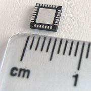

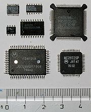
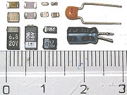
Surface mount components are usually smaller than their counterparts with leads, and are designed to be handled by machines rather than by humans. The electronics industry has standardized package shapes and sizes (the leading standardisation body is JEDEC
JEDEC
The JEDEC Solid State Technology Association, formerly known as the Joint Electron Devices Engineering Council , is an independent semiconductor engineering trade organization and standardization body...
). These include:
- Two-terminal packages
- Rectangular passive components (mostly resistorResistorA linear resistor is a linear, passive two-terminal electrical component that implements electrical resistance as a circuit element.The current through a resistor is in direct proportion to the voltage across the resistor's terminals. Thus, the ratio of the voltage applied across a resistor's...
s and capacitorCapacitorA capacitor is a passive two-terminal electrical component used to store energy in an electric field. The forms of practical capacitors vary widely, but all contain at least two electrical conductors separated by a dielectric ; for example, one common construction consists of metal foils separated...
s):- 01005 (0402 metric): 0.016 by 0.008 in (0.4064 by 0.2032 mm) Typical power rating for resistors 1/32 watt
- 0201 (0603 metric): 0.024 by 0.012 in (0.6096 by 0.3048 mm) Typical power rating for resistors 1/20 watt
- 0402 (1005 metric): 0.04 by 0.02 in (1 by 0.508 mm) Typical power rating for resistors 1/16 watt
- 0603 (1608 metric): 0.063 by 0.031 in (1.6 by 0.7874 mm) Typical power rating for resistors 1/16 watt
- 0805 (2012 metric): 0.08 by 0.05 in (2 by 1.3 mm) Typical power rating for resistors 1/10 watt
- 1206 (3216 metric): 0.126 by 0.063 in (3.2 by 1.6 mm) Typical power rating for resistors 1/8 watt
- 1210 (3225 metric): 0.126 by 0.1 in (3.2 by 2.5 mm) Typical power rating for resistors 1/4 watt
- 1806 (4516 metric): 0.177 by 0.063 in (4.5 by 1.6 mm)
- 1812 (4532 metric): 0.18 by 0.12 in (4.6 by 3 mm) Typical power rating for resistors 1/2 watt
- 2010 (5025 metric): 0.2 by 0.1 in (5.1 by 2.5 mm) Typical power rating for resistors 1/2 watt
- 2512 (6432 metric): 0.25 by 0.12 in (6.4 by 3 mm) Typical power rating for resistors 1 watt
- 2920 (7450 metric): 0.29 by 0.2 in (7.4 by 5.1 mm)
- Tantalum capacitorTantalum capacitorThe tantalum capacitor is a highly reliable type of electrolytic capacitor, available in both solid-bodied and separately encased forms. The encased "wet" variant is not used often in modern designs...
s:- EIA 3216-10 (Kemet I, AVX K): 3.2 mm × 1.6 mm × 1.0 mm
- EIA 3216-12 (Kemet S, AVX S): 3.2 mm × 1.6 mm × 1.2 mm
- EIA 3216-18 (Kemet A, AVX A): 3.2 mm × 1.6 mm × 1.8 mm
- EIA 3528-12 (Kemet T, AVX T): 3.5 mm × 2.8 mm × 1.2 mm
- EIA 3528-21 (Kemet B, AVX B): 3.5 mm × 2.8 mm × 2.1 mm
- EIA 6032-15 (Kemet U, AVX W): 6.0 mm × 3.2 mm × 1.5 mm
- EIA 6032-28 (Kemet C, AVX C): 6.0 mm × 3.2 mm × 2.8 mm
- EIA 7260-38 (Kemet E, AVX V): 7.2 mm × 6.0 mm × 3.8 mm
- EIA 7343-20 (Kemet V, AVX Y): 7.3 mm × 4.3 mm × 2.0 mm
- EIA 7343-31 (Kemet D, AVX D): 7.3 mm × 4.3 mm × 3.1 mm
- EIA 7343-43 (Kemet X, AVX E): 7.3 mm × 4.3 mm × 4.3 mm
- Aluminium capacitorsElectrolytic capacitorAn electrolytic capacitor is a type of capacitor that uses an electrolyte, an ionic conducting liquid, as one of its plates, to achieve a larger capacitance per unit volume than other types. They are often referred to in electronics usage simply as "electrolytics"...
:- (Panasonic / CDE A, Chemi-Con B): 3.3 mm × 3.3 mm
- (Panasonic B, Chemi-Con D): 4.3 mm × 4.3 mm
- (Panasonic C, Chemi-Con E): 5.3 mm × 5.3 mm
- (Panasonic D, Chemi-Con F): 6.6 mm × 6.6 mm
- (Panasonic E/F, Chemi-Con H): 8.3 mm × 8.3 mm
- (Panasonic G, Chemi-Con J): 10.3 mm × 10.3 mm
- (Chemi-Con K): 13.0 mm × 13.0 mm
- (Panasonic H): 13.5 mm × 13.5 mm
- (Panasonic J, Chemi-Con L): 17.0 mm × 17.0 mm
- (Panasonic K, Chemi-Con M): 19.0 mm × 19.0 mm
- SOD: Small Outline Diode
- SOD-523: 1.25 × 0.85 × 0.65 mm
- SOD-323 (SC-90): 1.7 × 1.25 × 0.95 mm
- SOD-123: 3.68 × 1.17 × 1.60 mm
- SOD-80C: 3.50 × 1.50 × More info
- MELFMELF Electronic ComponentsMELF is the acronym for metal electrode leadless face - a type of leadless cylindrical electronic surface mount device that is metallized at its ends...
(Metal Electrode Leadless Face): mostly resistorResistorA linear resistor is a linear, passive two-terminal electrical component that implements electrical resistance as a circuit element.The current through a resistor is in direct proportion to the voltage across the resistor's terminals. Thus, the ratio of the voltage applied across a resistor's...
s and diodeDiodeIn electronics, a diode is a type of two-terminal electronic component with a nonlinear current–voltage characteristic. A semiconductor diode, the most common type today, is a crystalline piece of semiconductor material connected to two electrical terminals...
s; barrel shaped components, dimensions do not match those of rectangular references for identical codes.- MicroMelf (MMU) Size 0102: L:2.2 mm D:1.1 mm (solder pad fits rectangular 0805) 1/5 watt (0.2 W) 100 V
- MiniMelf (MMA) Size 0204: L:3.6 mm D:1.4 mm (solder pad fits rectangular 1206) 1/4 watt (0.25 W) 200 V
- Melf (MMB) Size 0207: L:5.8 mm D:2.2 mm 1 watt (1.0 W) 500 V
- Rectangular passive components (mostly resistor
- Three terminal packages
- SOT: small-outline transistorTransistorA transistor is a semiconductor device used to amplify and switch electronic signals and power. It is composed of a semiconductor material with at least three terminals for connection to an external circuit. A voltage or current applied to one pair of the transistor's terminals changes the current...
, with three terminals- SOT-223: 6.7 mm × 3.7 mm × 1.8 mm body: four terminals, one of which is a large heat-transfer pad
- SOT-89: 4.5 mm × 2.5 mm × 1.5 mm body: four terminals, center pin is connected to a large heat-transfer pad
- SOT-23 (SC-59, TO-236-3): 2.9 mm × 1.3/1.75 mm × 1.3 mm body: three terminals for a transistor
- SOT-323 (SC-70): 2 mm × 1.25 mm × 0.95 mm body: three terminals
- SOT-416 (SC-75): 1.6 mm × 0.8 mm × 0.8 mm body: three terminals
- SOT-663: 1.6 mm × 1.6 mm × 0.55 mm body: three terminals
- SOT-723: 1.2 mm × 0.8 mm × 0.5 mm body: three terminals: flat lead
- SOT-883 (SC-101): 1 mm × 0.6 mm × 0.5 mm body: three terminals: leadless
- DPAK (TO-252): discrete packaging. Developed by MotorolaMotorolaMotorola, Inc. was an American multinational telecommunications company based in Schaumburg, Illinois, which was eventually divided into two independent public companies, Motorola Mobility and Motorola Solutions on January 4, 2011, after losing $4.3 billion from 2007 to 2009...
to house higher powered devices. Comes in three- or five-terminal versions - D2PAKD2PAKThe D2PAK or DDPAK, aka refers to a semiconductor package type intended for surface mounting on circuit boards. They are similar to the earlier TO-220-style packages intended for high power dissipation but lack the extended metal tab and mounting hole.As with all SMT packages, the pins on a D2PAK...
(TO-263): bigger than the DPAK; basically a surface mount equivalent of the TO220TO220The TO-220 is a style of electronic component package, commonly used for transistors, silicon-controlled rectifiers, and integrated circuits. The "TO" designation stands for "transistor outline". TO-220 packages have three leads. Similar packages with two, four, five or seven leads are also...
through-hole package. Comes in 3, 5, 6, 7, 8 or 9-terminal versions - D3PAK (TO-268): even larger than D2PAK
- SOT: small-outline transistor
- Five and six terminal packages
- SOT: small-outline transistor, with more than three terminals
- SOT-23-5 (SOT-25): 2.9 mm × 1.3/1.75 mm × 1.3 mm body: five terminals
- SOT-23-6 (SOT-26): 2.9 mm × 1.3/1.75 mm × 1.3 mm body: six terminals
- SOT-23-8 (SOT-28): 2.9 mm × 1.3/1.75 mm × 1.3 mm body: eight terminals
- SOT-353 (SC-88A): 2 mm × 1.25 mm × 0.95 mm body: five terminals
- SOT-363 (SC-88, SC-70-6): 2 mm × 1.25 mm × 0.95 mm body: six terminals
- SOT-563: 1.6 mm × 1.2 mm × 0.6 mm body: six terminals
- SOT-665: 1.6 mm × 1.6 mm × 0.55 mm body: six terminals
- SOT-666: 1.6 mm × 1.6 mm × 0.55 mm body: six terminals
- SOT-886: 1.5 mm × 1.05 mm × 0.5 mm body: six terminals: leadless
- SOT-891: 1.05 mm × 1.05 mm × 0.5 mm body: five terminals: leadless
- SOT-953: 1 mm × 1 mm × 0.5 mm body: five terminals
- SOT-963: 1 mm × 1 mm × 0.5 mm body: six terminals
- SOT: small-outline transistor, with more than three terminals
- Packages with higher terminal count (drawings of most of the following packages can be found on http://www.intersil.com/design/packages/plastic.asp)
- Dual-in-line
- Small-outline integrated circuitSmall-Outline Integrated CircuitA small-outline integrated circuit is a surface-mounted integrated circuit package which occupies an area about 30–50% less than an equivalent DIP, with a typical thickness that is 70% less. They are generally available in the same pinouts as their counterpart DIP ICs...
(SOIC): small-outline integrated circuitIntegrated circuitAn integrated circuit or monolithic integrated circuit is an electronic circuit manufactured by the patterned diffusion of trace elements into the surface of a thin substrate of semiconductor material...
, dual-in-line, 8 or more pins, gull-wing lead form, pin spacing 1.27 mm - J-Leaded Small Outline Package (SOJ): the same as SOIC except J-leaded http://www.siliconfareast.com/packages.htm
- TSOPThin small-outline packageThin small-outline packages, or TSOPs are a type of surface mount IC package. They are notably very low-profile and have tight lead spacing ....
: thin small-outline package, thinner than SOICSmall-Outline Integrated CircuitA small-outline integrated circuit is a surface-mounted integrated circuit package which occupies an area about 30–50% less than an equivalent DIP, with a typical thickness that is 70% less. They are generally available in the same pinouts as their counterpart DIP ICs...
with smaller pin spacing of 0.5 mm - SSOPShrink Small-Outline PackageShrink small-outline package is a microchip package for surface-mount technology. SSOP chips have "gull wing" leads protruding from the two long sides, and a lead spacing of 0.025 inches ....
: Shrink Small-Outline Package, pin spacing of 0.635 mm or in some cases 0.8 mm - TSSOPTSSOPA TSSOP is a rectangular, thin body size surface mount component. A Type I TSSOP has legs protruding from the width portion of the package. A Type II TSSOP has the legs protruding from the length portion of the package...
: Thin Shrink Small-Outline package. - QSOP: Quarter-Size Small-Outline package, with pin spacing of 0.635 mm
- VSOP: Very Small Outline Package, even smaller than QSOP; 0.4, 0.5 mm or 0.65 mm pin spacing
- DFN: Dual Flat No-lead, smaller footprint than leaded equivalent
- Small-outline integrated circuit
- Quad-in-line
- PLCCPlastic leaded chip carrierA plastic leaded chip carrier is a chip carrier with a equiangular plastic housing. It is a reduced cost evolution of the ceramic leadless chip carrier ....
: plastic leaded chip carrier, square, J-lead, pin spacing 1.27 mm - QFPQFPA QFP or Quad Flat Package is a surface mount integrated circuit package with leads extending from each of the four sides. Socketing such packages is rare and hole mounting is not possible. Versions ranging from 32 to 304 pins with a pitch ranging from 0.4 to 1.0 mm are common...
: Quad Flat Package, various sizes, with pins on all four sides - LQFPLQFPA Low-profile Quad Flat Package is a surface mount integrated circuit package format with component leads extending from each of the four sides. Pins are numbered counter-clockwise from the index dot. Spacing between pins can vary; common spacings are 0.4, 0.5, 0.65 and 0.80 mm intervals....
: Low-profile Quad Flat Package, 1.4 mm high, varying sized and pins on all four sides - PQFPPQFPPQFP, or plastic quad flat pack, is a type of IC packaging. PQFP is a special case of QFP, as is the thinner TQFP package.PQFP packages can vary in thickness from 2.0 mm to 3.8 mm.-References:*...
: plastic quad flat-pack, a square with pins on all four sides, 44 or more pins - CQFP: ceramic quad flat-pack, similar to PQFP
- MQFP: Metric Quad Flat Pack, a QFP package with metric pin distribution
- TQFPTQFPA thin quad flat pack is a type of surface-mounted package. TQFPs provide the same benefits of the metric QFP, but are thinner and have a standard lead-frame footprint ....
: thin quad flat pack, a thinner version of PQFP - QFNQFNFlat no-leads packages such as QFN and DFN physically and electrically connect integrated circuits to printed circuit boards. Flat no-leads, also known as MicroLeadFrame, is a surface-mount technology, one of several package technologies that connect ICs to the surfaces of PCBs without...
: Quad Flat No-lead, smaller footprint than leaded equivalent - LCCLeadless chip carrierA leadless chip carrier is a type of packaging for integrated circuits that has no "leads", but instead has rounded pins through the edges of the ceramic or molded plastic package....
: Leadless Chip Carrier, contacts are recessed vertically to "wick-in" solder. Common in aviation electronics because of robustness to mechanical vibration. - MLPMicro Leadframe PackageMicro leadframe package is a family of integrated circuit QFN packages, used in surface mounted electronic circuits designs. It is available in 3 versions which are MLPQ , MLPM , and MLPD . These package generally have an exposed die attach pad to improve thermal performance...
(MLF): Micro Leadframe Package (Micro Lead-Frame package) with a 0.5 mm contact pitch, no leads (same as QFN) http://www.carsem.com/services/mlp_dd.php - PQFN: Power Quad Flat No-lead, with exposed die-pad[s] for heatsinking
- PLCC
- Grid arrays
- PGAPin grid arrayA pin grid array, often abbreviated PGA, is a type of integrated circuit packaging. In a PGA, the package is square or roughly square, and the pins are arranged in a regular array on the underside of the package...
: Pin grid array. - BGABall grid arrayA ball grid array is a type of surface-mount packaging used for integrated circuits.- Description :The BGA is descended from the pin grid array , which is a package with one face covered with pins in a grid pattern. These pins conduct electrical signals from the integrated circuit to the printed...
: ball grid array, with a square or rectangular array of solder balls on one surface, ball spacing typically 1.27 mm - LGALand grid arrayThe land grid array is a type of surface-mount packaging for integrated circuits that is notable for having the pins on the socket rather than the integrated circuit...
: An array of bare lands only. Similar to in appearance to QFNQFNFlat no-leads packages such as QFN and DFN physically and electrically connect integrated circuits to printed circuit boards. Flat no-leads, also known as MicroLeadFrame, is a surface-mount technology, one of several package technologies that connect ICs to the surfaces of PCBs without...
, but mating is by spring pins within a socket rather than solder. - FBGA: fine pitch ball grid array, with a square or rectangular array of solder balls on one surface
- LFBGA: low profile fine pitch ball grid array, with a square or rectangular array of solder balls on one surface, ball spacing typically 0.8 mm
- TFBGA: thin fine pitch ball grid array, with a square or rectangular array of solder balls on one surface, ball spacing typically 0.5 mm
- CGA: column grid array, circuit package in which the input and output points are high temperature solder cylinders or columns arranged in a grid pattern.
- CCGA: ceramic column grid array, circuit package in which the input and output points are high temperature solder cylinders or columns arranged in a grid pattern. The body of the component is ceramic.
- μBGA: micro-BGA, with ball spacing less than 1 mm
- LLP: Lead Less Package, a package with metric pin distribution (0.5 mm pitch).
- PGA
- Non-packaged devices (although surface mount, these devices require specific process for assembly):
- COB: chip-on-board; a bare siliconSiliconSilicon is a chemical element with the symbol Si and atomic number 14. A tetravalent metalloid, it is less reactive than its chemical analog carbon, the nonmetal directly above it in the periodic table, but more reactive than germanium, the metalloid directly below it in the table...
chip, that is usually an integrated circuit, is supplied without a package (usually a lead frame overmolded with epoxyEpoxyEpoxy, also known as polyepoxide, is a thermosetting polymer formed from reaction of an epoxide "resin" with polyamine "hardener". Epoxy has a wide range of applications, including fiber-reinforced plastic materials and general purpose adhesives....
) and is attached, often with epoxy, directly to a circuit board. The chip is then wire bondedWire bondingWire bonding is the primary method of making interconnections between an integrated circuit and a printed circuit board during semiconductor device fabrication. Although less common, wire bonding can be used to connect an IC to other electronics or to connect from one PCB to another...
and protected from mechanical damage and contamination by an epoxy "glob-top". - COF: chip-on-flex; a variation of COB, where a chip is mounted directly to a flex circuit.
- COG: chip-on-glass; a variation of COB, where a chip is mounted directly to a piece of glass: typically an LCD.
- COB: chip-on-board; a bare silicon
- Dual-in-line
There are often subtle variations in package details from manufacturer to manufacturer, and even though standard designations are used, designers need to confirm dimensions when laying out printed circuit boards.
Identification
ResistorsSMD resistors usually are marked with their resistance values using three digits, two significant digits and a multiplier digit. These are quite often white lettering on a black background, but other coloured backgrounds and lettering can be used.
The black or coloured coating is usually only on one face of the device, the sides and other face simply being the uncoated, usually white ceramic substrate. The coated surface, with the resistive element beneath is normally positioned face up when the device is soldered to the board although they can rarely be seen mounted with the uncoated underside face up, whereby the resistance value code is not visible.
- Typical examples of resistance codes
- 102 = 10 00 = 1000 Ohms = 1K Ohm
- 0R2 = 0.2 Ohms
- 684 = 68 0000 = 680 000 Ohms = 680K Ohms
Capacitors
Non electrolytic capacitors are usually unmarked and the only reliable method of determining their value is removal from the circuit and subsequent measurement with a capacitance meter or impedance bridge.
The materials used to fabricate the capacitors, such as Nickel Tantalate, possess different colours and these can give an approximate idea of the capacitance of the component.
- Light grey body colour indicates a capacitance which is generally less than 100pF.
- Medium Grey colour indicates a capacitance anywhere from 10pF to 10nF.
- Light brown colour indicates a capacitance in a range from 1nF to 100nF.
- Medium brown colour indicates a capacitance in a range from 10nF to 1μF.
- Dark brown colour indicates a capacitance from 100nF to 10μF.
- Dark grey colour indicates a capacitance in the μF range, generally 0.5 to 50μF, or the device may be an inductor and the dark grey is the colour of the ferrite bead. (An inductor will measure a low resistance to a multimeter on the resistance range whereas a capacitor, out of the circuit, will measure a near infinite resistance.)
Generally the larger the size, the larger the capacitance or voltage rating all other things being the same. So a 100nF, 50v capacitor may well look the same as a 10nF, 500v device, however the 500v rated device will be used in a high voltage or high energy part of the circuit where as the 50v rated device would be found throughout the small signal part of the circuit.
SMD (non electrolytic) capacitors, which are usually monolithic ceramic capacitors, exhibit the same body colour on all four faces not covered by the end caps.
SMD electrolytic capacitors, usually tantalum capacitors, and film capacitors are marked like resistors, with two significant figures and a multiplier in units of pico Farads or pF, (10-12 Farad.)
- Examples
- 104 = 100nF = 100 000pF
- 226 = 22μF = 22 000 000pF
The electrolytic capacitors are usually encapsulated in black or beige epoxy resin with flat metal connecting strips bent underneath.
Some film or tantalum electrolytic types are unmarked and possess red, orange or blue body colours with complete end caps, not metal strips.
Inductors
Due to the small dimensions of SMDs, inductors are limited to quite small values, generally less than 1mH. Smaller inductances with moderately high current ratings are usually of the ferrite bead type. They are simply a metal conductor passing through a ferrite bead and almost the same as their through-hole versions but possess the SMD end caps rather than leads. They appear dark grey and are magnetic, unlike capacitors with a similar dark grey appearance. These ferrite bead type are limited to small values in the nH, (nano Henry), range and are often used as power supply rail decouplers or in high frequency parts of a circuit.
Inductors with larger inductance values will often possess turns of wire or flat strap around the body or embedded in clear epoxy. This wire or strap can often be easily seen and sometimes a ferrite core is present also. These higher inductance types are often limited to small current ratings although some of the flat strap types can handle a few amps.
Like capacitors, the specific values are not usually marked and removal from the circuit and subsequent measurement is the only really reliable way of determining their value.
Discrete Semiconductors
Discrete semiconductors, such as transistors, diodes and F.E.T.s are often marked with a cryptic two or three symbol code in which the same code marked on different packages or on devices made by different manufacturers can translate to different devices.
Many of these codes, used because the devices are too small to be marked with more traditional numbers used on through-hole equivalent devices, correlate to more familiar traditional part numbers when a correlation list is consulted.
GM4PMK in the United Kingdom has prepared a correlation list, http://www.marsport.org.uk/smd/mainframe.htm and a similar .pdf list is also avalable, elektronik.googlecode.com/files/SMD_Catalog222.pdf, although these lists do not contain all the device codes one might encounter.
Integrated Circuits
Generally integrated circuit packages are large enough to print the whole number or a significant part of the number which can be fully identified as long as you can identify the manufacturer of the device.
- Examples
- 4066 = Philips HEF4066, or if Motorola, MC14066. (Quad Analog Switch.)
- 5502M = Fujitsu Electric FA5502. (Boost Architecture Power Factor CorrectionPFC- Science :*Perfluorinated compounds, a class of organofluorine compounds that have all hydrogen replaced with fluorine*Perfluorocarbons, fluorocarbon compounds derived from hydrocarbons...
controller.)
See also
- Board to board connectorsBoard to board connectorsBoard to board connectors are used to connect printed circuit boards , electronic components that contain a conductive pattern printed on the surface of the insulating base in an accurate and repeatable manner...
- Chip carrierChip carrierA chip carrier, also known as a chip container or chip package, is a container for a transistor or an integrated circuit. The carrier usually provides metal leads, or "pins", which are sturdy enough to electrically and mechanically connect the fragile chip to a circuit board. This connection may be...
- ElectronicsElectronicsElectronics is the branch of science, engineering and technology that deals with electrical circuits involving active electrical components such as vacuum tubes, transistors, diodes and integrated circuits, and associated passive interconnection technologies...
- Electronics Manufacturing ServicesElectronics Manufacturing ServicesElectronic manufacturing services is a term used for companies that design, test, manufacture, distribute, and provide return/repair services for electronic components and assemblies for original equipment manufacturers...
- List of electronics package dimensions
- Plastic leaded chip carrierPlastic leaded chip carrierA plastic leaded chip carrier is a chip carrier with a equiangular plastic housing. It is a reduced cost evolution of the ceramic leadless chip carrier ....
- Point-to-point constructionPoint-to-point constructionPoint-to-point construction refers to the method in which electronics circuits were constructed before the 1950s. Point-to-point construction is still used to construct prototype equipment with few or heavy electronic components....
- Printed circuit boardPrinted circuit boardA printed circuit board, or PCB, is used to mechanically support and electrically connect electronic components using conductive pathways, tracks or signal traces etched from copper sheets laminated onto a non-conductive substrate. It is also referred to as printed wiring board or etched wiring...
- RoHS
- SMT placement equipmentSMT Placement EquipmentSMT component placement systems, commonly called pick-and-place machines or P&Ps, are robotic machines which are used to place surface-mount devices onto a printed circuit board...
- Through-hole technologyThrough-hole technologyThrough-hole technology, also spelled "thru-hole", refers to the mounting scheme used for electronic components that involves the use of leads on the components that are inserted into holes drilled in printed circuit boards and soldered to pads on the opposite side either by manual assembly by...
- Wire wrapWire wrapWire wrap is a technology used to assemble electronics. It is a method to construct circuit boards without having to make a printed circuit board. Wires can be wrapped by hand or by machine, and can be hand-modified afterwards. It was popular for large-scale manufacturing in the 60s and early 70s,...