

Superlattice
Encyclopedia
Superlattice is a periodic structure of layers of two (or more) materials. Typically, the thickness of one layer is several nanometers
.
of dislocation
s cannot operate anymore in any of the nanolayers.
The increased mechanical hardness of such superlattice materials has been confirmed numerous times since then, e.g. on hard PVD coatings by Barnett and Sproul (and several other research teams as well).
, each quantum wells sets up a new set of selection rules which affects the conditions for charges to flow through the structure. The two different semiconductor materials are deposited alternately on each other to form a periodic structure in the growth direction. Since the first proposal by Leo Esaki
and Raphael Tsu
of synthetic artificial superlattices in 1970, great advances in the physics of such ultra-fine semiconductors, presently called quantum structures, have been made within the past two decades. The concept of quantum confinement has led to the observation of quantum size effects in isolated quantum well heterostructures and is closely related to superlattices through the tunneling phenomena. Therefore, these two ideas are often discussed on the same physical basis, but each field has its own intrigue and different physics useful for applications in many electric and optical devices.
There also exists a class of quasiperiodic superlattices named after Fibonacci
. A Fibonacci superlattice can be viewed as a one-dimensional quasicrystal
, where either electron hopping transfer or on-site energy takes two values arranged in a Fibonacci sequence.
 Semiconductor materials, which are actually used to fabricate the superlattice structures, may be divided by the element groups, IV, III-V and II-VI. While the group III-V semiconductors have been extensively studied, group IV heterostructures such as the SixGe1-x system are much more difficult to realize because of the large lattice mismatch. Nevertheless, the strain modification of the subband structures is interesting in these quantum structures and has attracted much attention.
So far mostly the III-V compound semiconductors represented by the GaAs/AlxGa1-xAs heterostructures have been investigated. In particular, one distinguished merit of the GaAs/AlAs system is that the difference in lattice constant between GaAs and AlAs is very small despite the highly corrosive nature of AlAs. In addition, the difference of their thermal expansion coefficient is also small. Thus, the strain remaining at room temperature can be minimized after cooling down from the higher epitaxial growth temperatures. The first compositional superlattice was realized using the GaAs/AlxGa1-xAs material system.
Superlattices can be produced using various techniques, but the most common are molecular-beam epitaxy (MBE) and sputtering
. With these methods, layers can be produced with thicknesses of only a few atomic spacings. An example of specifying a superlattice is [Fe20V30]20. It describes a bi-layer of 20Å of Iron (Fe) and 30Å of Vanadium (V) repeated 20 times, thus yielding a total thickness of 1000Å or 100 nm. The MBE technology as a means of fabricating semiconductor superlattice is of primary importance. In addition to the MBE technology, metal-organic chemical vapor deposition (MO-CVD) has also contributed to the development of superconductor superlattices, which are composed of quaternary III-V compound semiconductors like InGaAsP alloys. More recently, a combination of gas source handling and ultrahigh vacuum (UHV) technologies such as metal-organic molecules as source materials, are becoming popular as well as gas-source MBE using hybrid gases like arsine (AsH3) and phosphine (PH3).
Generally speaking MBE is a method of using three temperatures in binary systems, e.g., the substrate temperature and the source material temperature of the group III and the group V elements in the case of III-V compounds.
The structural quality of the produced superlattices can be verified by means of X-ray diffraction or neutron diffraction
spectra which contain characteristic satellite peaks. Other effects associated with the alternating layering are: giant magnetoresistance, tunable reflectivity for X-ray and Neutron mirrors, neutron spin polarization
, and changes in the elastic and acoustic properties. Depending on the nature of its components, a superlattice may be called magnetic, optical or semiconducting.
 ). When a and b are not too small compared with the interatomic spacing, an adequate approximation is obtained by replacing these fast varying potentials by an effective potential derived from the band structure of the original bulk semiconductors. It is straightforward to solve 1D Schrödinger equations in each of the individual layers, whose solutions
  are linear combinations of real or imaginary exponentials.
For a large barrier thickness, tunneling is a weak perturbation with regard to the uncoupled dispersionless states, which are fully confined as well. In this case the dispersion relation , periodic over
  with over
  by virtue of the Bloch theorem, is fully sinusoidal:
and the effective mass changes sign for :
:
In the case of minibands, this sinusoidal character is no longer preserved. Only high up in the miniband (for wavevectors well beyond ) is the top actually 'sensed' and does the effective mass change sign. The very shape of the miniband dispersion obviously influences miniband transport profoundly, and accurate dispersion relation calculations are indispensable in the case of wide minibands. It is worth mentioning here that the condition for observing single miniband transport is the absence of any interminiband transfer by any process. This means in particular that the thermal quantum kBT should be much smaller than the energy difference
  between the first and second miniband, even in the presence of the applied electric field.
 and a z-dependent function
  which satisfies the eigenvalue equation
 .
.
As and
and  are periodic functions with the superlattice period d, the eigenstates are Bloch state
  with energy
  . Within first-order perturbation theory in k2, one obtains the energy
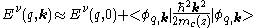 .
.
Now, will exhibit a larger probability in the well, so that it seems reasonable to replace the second term by

where is the effective mass of the quantum well.
are delocalized over the whole superlattice structure. This may provide difficulties if electric fields are applied or effects due to the finite length of the superlattice are considered. Therefore, it is often helpful to use different sets of basis states which are better localized. A tempting choice would be the use of eigenstates of single quantum wells. Nevertheless such a choice has a severe shortcoming: the corresponding states are solutions of two different Hamiltonians, each neglecting the presence of the other well. Thus these states are not orthogonal which provides complications. Typically, the coupling is estimated by the transfer Hamiltonian within this approach.
For these reasons, it is more convenient to use the set of Wannier functions.
In this case, we can easily see that if there exists an eigenstate with wavefunction and energy
  , then the set of states corresponding to wavefunctions
 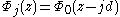 are eigenstates of the Hamiltonian with energies Ej = E0 − jeFd as well. These states are equally spaced both in energy and real space and form the so-called Wannier–Stark ladder. This feature has to be considered with some care, as the potential
  is not bounded for the infnite crystal, which implies a continuous energy spectrum. Nevertheless, the characteristic energy spectrum of these Wannier–Stark ladders could be resolved experimentally in semiconductor superlattices.
 The motion of charge carriers in a superlattice is different from that in the individual layers: mobility
of charge carriers can be enhanced, which is beneficial for high-frequency devices, and specific optical properties are used in semiconductor laser
s.
If an external bias is applied to a conductor, such as a metal or a semiconductor, typically an electrical current is generated. The magnitude of this current is determined by the band structure of the material, scattering processes, the applied field strength, as well as the equilibrium carrier distribution of the conductor.
A particular case of superlattices called superstripes
are made of superconducting units separated by spacers. In each miniband the superconducting order parameter, called the superconducting gap, takes different values producing a multi-gap, or two-gap or multiband superconductivity.
Nanometre
A nanometre is a unit of length in the metric system, equal to one billionth of a metre. The name combines the SI prefix nano- with the parent unit name metre .The nanometre is often used to express dimensions on the atomic scale: the diameter...
.
Discovery
Superlattices were discovered early in the 20th century through their special X-ray diffraction patterns.Mechanical properties
It has been theoretically predicted by J.S. Koehler that, by using alternate (nano-)layers of materials with high and low elastic constants, the mechanical resistance of the material to shearing is improved by up to 100 times as the Frank-Read sourceFrank-Read Source
A Frank-Read Source is a mechanism explaining the generation of multiple dislocations in specific well spaced slip planes in crystals when they are deformed. It was proposed by and named after Sir Charles Frank and Thornton Read. When a crystal is deformed, slip is found to occur only on certain...
of dislocation
Dislocation
In materials science, a dislocation is a crystallographic defect, or irregularity, within a crystal structure. The presence of dislocations strongly influences many of the properties of materials...
s cannot operate anymore in any of the nanolayers.
The increased mechanical hardness of such superlattice materials has been confirmed numerous times since then, e.g. on hard PVD coatings by Barnett and Sproul (and several other research teams as well).
Semiconductor properties
If the superlattice is made of two semiconductor materials with different band gapBand gap
In solid state physics, a band gap, also called an energy gap or bandgap, is an energy range in a solid where no electron states can exist. In graphs of the electronic band structure of solids, the band gap generally refers to the energy difference between the top of the valence band and the...
, each quantum wells sets up a new set of selection rules which affects the conditions for charges to flow through the structure. The two different semiconductor materials are deposited alternately on each other to form a periodic structure in the growth direction. Since the first proposal by Leo Esaki
Leo Esaki
Reona Esaki also known as Leo Esaki is a Japanese physicist who shared the Nobel Prize in Physics in 1973 with Ivar Giaever and Brian David Josephson for his discovery of the phenomenon of electron tunneling. He is known for his invention of the Esaki diode, which exploited that phenomenon...
and Raphael Tsu
Raphael Tsu
Raphael Tsu is a Fellow of the American Physical Society and currently serves as a Distinguished Professor of electrical engineering at the University of North Carolina at Charlotte, Charlotte, NC.-Biography:...
of synthetic artificial superlattices in 1970, great advances in the physics of such ultra-fine semiconductors, presently called quantum structures, have been made within the past two decades. The concept of quantum confinement has led to the observation of quantum size effects in isolated quantum well heterostructures and is closely related to superlattices through the tunneling phenomena. Therefore, these two ideas are often discussed on the same physical basis, but each field has its own intrigue and different physics useful for applications in many electric and optical devices.
Semiconductor superlattice types
The superlattice miniband structures are divided into three different types, called type I, type II and type III. For the type I heterostructures the bottom of the conduction subband and the top of the valence subband are formed in the same semiconductor layer. In the type II the conduction and valence subbands are staggered in both real and reciprocal space, so that electrons and holes are confined in different layers. Type III superlattice involves semimetal material, one example is HgTe/CdTe superlattice. Although the bottom of the conduction subband and the top of the valence subband are formed in the same semiconductor layer in Type III superlattice, which is similar with Type I superlattice, the band gap of Type III superlattice can be continuously adjusted from semiconductor to zero band gap material and to semimetal with negative band gap.There also exists a class of quasiperiodic superlattices named after Fibonacci
Fibonacci
Leonardo Pisano Bigollo also known as Leonardo of Pisa, Leonardo Pisano, Leonardo Bonacci, Leonardo Fibonacci, or, most commonly, simply Fibonacci, was an Italian mathematician, considered by some "the most talented western mathematician of the Middle Ages."Fibonacci is best known to the modern...
. A Fibonacci superlattice can be viewed as a one-dimensional quasicrystal
Quasicrystal
A quasiperiodic crystal, or, in short, quasicrystal, is a structure that is ordered but not periodic. A quasicrystalline pattern can continuously fill all available space, but it lacks translational symmetry...
, where either electron hopping transfer or on-site energy takes two values arranged in a Fibonacci sequence.
Semiconductor superlattice materials and growth technology
So far mostly the III-V compound semiconductors represented by the GaAs/AlxGa1-xAs heterostructures have been investigated. In particular, one distinguished merit of the GaAs/AlAs system is that the difference in lattice constant between GaAs and AlAs is very small despite the highly corrosive nature of AlAs. In addition, the difference of their thermal expansion coefficient is also small. Thus, the strain remaining at room temperature can be minimized after cooling down from the higher epitaxial growth temperatures. The first compositional superlattice was realized using the GaAs/AlxGa1-xAs material system.
Superlattices can be produced using various techniques, but the most common are molecular-beam epitaxy (MBE) and sputtering
Sputtering
Sputtering is a process whereby atoms are ejected from a solid target material due to bombardment of the target by energetic particles. It is commonly used for thin-film deposition, etching and analytical techniques .-Physics of sputtering:...
. With these methods, layers can be produced with thicknesses of only a few atomic spacings. An example of specifying a superlattice is [Fe20V30]20. It describes a bi-layer of 20Å of Iron (Fe) and 30Å of Vanadium (V) repeated 20 times, thus yielding a total thickness of 1000Å or 100 nm. The MBE technology as a means of fabricating semiconductor superlattice is of primary importance. In addition to the MBE technology, metal-organic chemical vapor deposition (MO-CVD) has also contributed to the development of superconductor superlattices, which are composed of quaternary III-V compound semiconductors like InGaAsP alloys. More recently, a combination of gas source handling and ultrahigh vacuum (UHV) technologies such as metal-organic molecules as source materials, are becoming popular as well as gas-source MBE using hybrid gases like arsine (AsH3) and phosphine (PH3).
Generally speaking MBE is a method of using three temperatures in binary systems, e.g., the substrate temperature and the source material temperature of the group III and the group V elements in the case of III-V compounds.
The structural quality of the produced superlattices can be verified by means of X-ray diffraction or neutron diffraction
Neutron diffraction
Neutron diffraction or elastic neutron scattering is the application of neutron scattering to the determination of the atomic and/or magnetic structure of a material: A sample to be examined is placed in a beam of thermal or cold neutrons to obtain a diffraction pattern that provides information of...
spectra which contain characteristic satellite peaks. Other effects associated with the alternating layering are: giant magnetoresistance, tunable reflectivity for X-ray and Neutron mirrors, neutron spin polarization
Spin polarization
Spin polarization is the degree to which the spin, i.e., the intrinsic angular momentum of elementary particles, is aligned with a given direction. This property may pertain to the spin, hence to the magnetic moment, of conduction electrons in ferromagnetic metals, such as iron, giving rise to...
, and changes in the elastic and acoustic properties. Depending on the nature of its components, a superlattice may be called magnetic, optical or semiconducting.
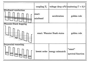
Miniband structure
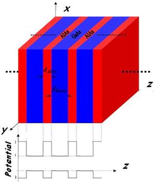
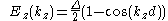
The schematic structure of a periodic superlattice is shown below, where A and B are two different semiconductor materials of respective layer thickness a and b (period:). When a and b are not too small compared with the interatomic spacing, an adequate approximation is obtained by replacing these fast varying potentials by an effective potential derived from the band structure of the original bulk semiconductors. It is straightforward to solve 1D Schrödinger equations in each of the individual layers, whose solutions are linear combinations of real or imaginary exponentials.For a large barrier thickness, tunneling is a weak perturbation with regard to the uncoupled dispersionless states, which are fully confined as well. In this case the dispersion relation
, periodic over with over by virtue of the Bloch theorem, is fully sinusoidal:and the effective mass changes sign for
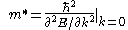
:In the case of minibands, this sinusoidal character is no longer preserved. Only high up in the miniband (for wavevectors well beyond
) is the top actually 'sensed' and does the effective mass change sign. The very shape of the miniband dispersion obviously influences miniband transport profoundly, and accurate dispersion relation calculations are indispensable in the case of wide minibands. It is worth mentioning here that the condition for observing single miniband transport is the absence of any interminiband transfer by any process. This means in particular that the thermal quantum kBT should be much smaller than the energy difference between the first and second miniband, even in the presence of the applied electric field.Bloch states
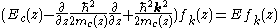
For an ideal superlattice a complete set of eigenstates states can be constructed by products of plane waves and a z-dependent function which satisfies the eigenvalue equation.As
and are periodic functions with the superlattice period d, the eigenstates are Bloch state with energy . Within first-order perturbation theory in k2, one obtains the energy.Now,
will exhibit a larger probability in the well, so that it seems reasonable to replace the second term bywhere
is the effective mass of the quantum well.Wannier functions
By definition the Bloch functionsBloch wave
A Bloch wave or Bloch state, named after Felix Bloch, is the wavefunction of a particle placed in a periodic potential...
are delocalized over the whole superlattice structure. This may provide difficulties if electric fields are applied or effects due to the finite length of the superlattice are considered. Therefore, it is often helpful to use different sets of basis states which are better localized. A tempting choice would be the use of eigenstates of single quantum wells. Nevertheless such a choice has a severe shortcoming: the corresponding states are solutions of two different Hamiltonians, each neglecting the presence of the other well. Thus these states are not orthogonal which provides complications. Typically, the coupling is estimated by the transfer Hamiltonian within this approach.
For these reasons, it is more convenient to use the set of Wannier functions.
Wannier–Stark ladder
If an electric field F is applied to the superlattice structure the Hamiltonian exhibits an additional scalar potential eφ(z) = −eFz which destroys the translational invariance.In this case, we can easily see that if there exists an eigenstate with wavefunction
and energy , then the set of states corresponding to wavefunctions are eigenstates of the Hamiltonian with energies Ej = E0 − jeFd as well. These states are equally spaced both in energy and real space and form the so-called Wannier–Stark ladder. This feature has to be considered with some care, as the potential is not bounded for the infnite crystal, which implies a continuous energy spectrum. Nevertheless, the characteristic energy spectrum of these Wannier–Stark ladders could be resolved experimentally in semiconductor superlattices.Superlattice transport
Electron mobility
In solid-state physics, the electron mobility characterizes how quickly an electron can move through a metal or semiconductor, when pulled by an electric field. In semiconductors, there is an analogous quantity for holes, called hole mobility...
of charge carriers can be enhanced, which is beneficial for high-frequency devices, and specific optical properties are used in semiconductor laser
Laser
A laser is a device that emits light through a process of optical amplification based on the stimulated emission of photons. The term "laser" originated as an acronym for Light Amplification by Stimulated Emission of Radiation...
s.
If an external bias is applied to a conductor, such as a metal or a semiconductor, typically an electrical current is generated. The magnitude of this current is determined by the band structure of the material, scattering processes, the applied field strength, as well as the equilibrium carrier distribution of the conductor.
A particular case of superlattices called superstripes
Superstripes
Superstripes are metallic heterostructures at the atomic limit where the shape resonance in the energy gap parameters ∆n is the driving mechanism for the amplification of the superconductivity critical temperature...
are made of superconducting units separated by spacers. In each miniband the superconducting order parameter, called the superconducting gap, takes different values producing a multi-gap, or two-gap or multiband superconductivity.