In
digital circuitDigital electronics represent signals by discrete bands of analog levels, rather than by a continuous range. All levels within a band represent the same signal state...
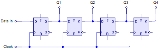
s, a
shift register is a cascade of
flip flopIn electronics, a flip-flop or latch is a circuit that has two stable states and can be used to store state information. The circuit can be made to change state by signals applied to one or more control inputs and will have one or two outputs. It is the basic storage element in sequential logic...
s, sharing the same clock, which has the output of any one but the last flip-flop connected to the "data" input of the next one in the chain, resulting in a circuit that shifts by one position the one-dimensional "
bit array" stored in it,
shifting in the data present at its input and
shifting out the last bit in the array, when enabled to do so by a transition of the clock input. More generally, a
shift register may be multidimensional, such that its "data in" input and stage outputs are themselves bit arrays: this is implemented simply by running several shift registers of the same bit-length in parallel.
Shift registers can have both parallel and
serialIn telecommunication and computer science, serial communication is the process of sending data one bit at a time, sequentially, over a communication channel or computer bus. This is in contrast to parallel communication, where several bits are sent as a whole, on a link with several parallel channels...
inputs and outputs. These are often configured as
serial-in, parallel-out (SIPO) or as
parallel-in, serial-out (PISO). There are also types that have both serial and parallel input and types with serial and parallel output. There are also
bi-directional shift registers which allow shifting in both directions: L→R or R→L. The serial input and last output of a shift register can also be connected together to create a
circular shift register.
Destructive readout
| 0 |
0 |
0 |
0 |
| 1 |
0 |
0 |
0 |
| 0 |
1 |
0 |
0 |
| 1 |
0 |
1 |
0 |
| 1 |
1 |
0 |
1 |
| 0 |
1 |
1 |
0 |
| 0 |
0 |
1 |
1 |
| 0 |
0 |
0 |
1 |
| 0 |
0 |
0 |
0 |
These are the simplest kind of shift registers. The data string is presented at 'Data In', and is shifted right one stage each time 'Data Advance' is brought high. At each advance, the bit on the far left (i.e. 'Data In') is shifted into the first
flip-flopIn electronics, a flip-flop or latch is a circuit that has two stable states and can be used to store state information. The circuit can be made to change state by signals applied to one or more control inputs and will have one or two outputs. It is the basic storage element in sequential logic...
's output. The bit on the far right (i.e. 'Data Out') is shifted out and lost.
The data are stored after each
flip-flopIn electronics, a flip-flop or latch is a circuit that has two stable states and can be used to store state information. The circuit can be made to change state by signals applied to one or more control inputs and will have one or two outputs. It is the basic storage element in sequential logic...
on the 'Q' output, so there are four storage 'slots' available in this arrangement, hence it is a 4-Bit Register. To give an idea of the shifting pattern, imagine that the register holds 0000 (so all storage slots are empty). As 'Data In' presents 1,0,1,1,0,0,0,0 (in that order, with a pulse at 'Data Advance' each time — this is called clocking or strobing) to the register, this is the result. The left hand column corresponds to the left-most flip-flop's output pin, and so on.
So the serial output of the entire register is 10110000 . As you can see if we were to continue to input data, we would get exactly what was put in, but offset by four 'Data Advance' cycles. This arrangement is the hardware equivalent of a queue. Also, at any time, the whole register can be set to zero by bringing the reset (R) pins high.
This arrangement performs
destructive readout - each datum is lost once it has been shifted out of the right-most bit.
Serial-in, parallel-out (SIPO)
This configuration allows conversion from serial to parallel format. Data is input serially, as described in the SISO section above. Once the data has been input, it may be either read off at each output simultaneously, or it can be shifted out and replaced.
Parallel-in, Serial-out (PISO)
This configuration has the data input on lines D1 through D4 in parallel format. To write the data to the register, the Write/Shift control line must be held LOW. To shift the data, the W/S control line is brought HIGH and the registers are clocked. The arrangement now acts as a SISO shift register, with D1 as the Data Input. However, as long as the number of clock cycles is not more than the length of the data-string, the Data Output, Q, will be the parallel data read off in order.
The animation below shows the write/shift sequence, including the internal state of the shift register.
Uses
One of the most common uses of a shift register is to convert between serial and parallel interfaces. This is useful as many circuits work on groups of bits in parallel, but serial interfaces are simpler to construct. Shift registers can be used as simple delay circuits. Several bidirectional shift registers could also be connected in parallel for a hardware implementation of a
stackIn computer science, a stack is a last in, first out abstract data type and linear data structure. A stack can have any abstract data type as an element, but is characterized by only three fundamental operations: push, pop and stack top. The push operation adds a new item to the top of the stack,...
.
SIPO registers are commonly attached to the output of microprocessors when more output pins are required than are available. This allows several binary devices to be controlled using only two or three pins - the devices in question are attached to the parallel outputs of the shift register, then the desired state of all those devices can be sent out of the microprocessor using a single serial connection. Similarly, PISO configurations are commonly used to add more binary inputs to a microprocessor than are available - each binary input (i.e. a switch or button, or more complicated circuitry designed to output high when active) is attached to a parallel input of the shift register, then the data is sent back via serial to the microprocessor using several fewer lines than originally required.
Shift registers can be used also as pulse extenders. Compared to monostable multivibrators, the timing has no dependency on component values, however it requires external clock and the timing accuracy is limited by a granularity of this clock. Example: Ronja Twister, where five 74164 shift registers create the core of the timing logic this way (
schematic).
In early computers, shift registers were used to handle data processing: two numbers to be added were stored in two shift registers and clocked out into an
arithmetic and logic unit (ALU)In computing, an arithmetic logic unit is a digital circuit that performs arithmetic and logical operations.The ALU is a fundamental building block of the central processing unit of a computer, and even the simplest microprocessors contain one for purposes such as maintaining timers...
with the result being fed back to the input of one of the shift registers (the accumulator) which was one bit longer since binary addition can only result in an answer that is the same size or one bit longer.
Many computer languages include instructions to 'shift right' and 'shift left' the data in a register, effectively dividing by two or multiplying by two for each place shifted.
Very large serial-in serial-out shift registers (thousands of bits in size) were used in a similar manner to the earlier
delay line memoryDelay line memory was a form of computer memory used on some of the earliest digital computers. Like many modern forms of electronic computer memory, delay line memory was a refreshable memory, but as opposed to modern random-access memory, delay line memory was serial-access...
in some devices built in the early 1970s. Such memories were sometimes called
circulating memory. For example, the
DataPoint 3300The DataPoint 3300 was the first computer terminal manufactured by the Computer Terminal Corporation , announced in 1967 and shipping in 1969...
terminal stored its display of 25 rows of
72 columnsIn typography and computing characters per line or terminal width refers to the maximal number of monospaced characters that may appear on a single line...
of upper-case characters using fifty-four 200-bit shift registers, arranged in six tracks of nine packs each, providing storage for 1800 six-bit characters. The shift register design meant that scrolling the terminal display could be accomplished by simply pausing the display output to skip one line of characters.
History
One of the first known examples of a shift register was in the
ColossusNot to be confused with the fictional computer of the same name in the movie Colossus: The Forbin Project.Colossus was the world's first electronic, digital, programmable computer. Colossus and its successors were used by British codebreakers to help read encrypted German messages during World War II...
, a code-breaking machine of the 1940s. It was a five-stage device built of
vacuum tubeIn electronics, a vacuum tube, electron tube , or thermionic valve , reduced to simply "tube" or "valve" in everyday parlance, is a device that relies on the flow of electric current through a vacuum...
s and
thyratronA thyratron is a type of gas filled tube used as a high energy electrical switch and controlled rectifier. Triode, tetrode and pentode variations of the thyratron have been manufactured in the past, though most are of the triode design...
s.
See also
- linear feedback shift register
A linear feedback shift register is a shift register whose input bit is a linear function of its previous state.The most commonly used linear function of single bits is XOR...
(LFSR)
- Ring counter
A ring counter is a type of counter composed of a circular shift register. The output of the last shift register is fed to the input of the first register.There are two types of ring counters:...
- Serial Peripheral Interface Bus
The Serial Peripheral Interface Bus or SPI bus is a synchronous serial data link standard named by Motorola that operates in full duplex mode. Devices communicate in master/slave mode where the master device initiates the data frame. Multiple slave devices are allowed with individual slave select ...
- Shift register lookup table (SRL)
External links