

SONOS
Encyclopedia
SONOS, short for "Silicon-Oxide-Nitride-Oxide-Silicon", is a type of non-volatile
computer memory
closely related to Flash RAM. It is distinguished from mainstream flash by the use of silicon nitride
(Si3N4) instead of polysilicon for the charge storage material. A further variant is "SHINOS" ("Silicon Hi-k
Nitride Oxide Silicon"). SONOS promises lower programming voltages and higher program/erase cycle endurance than polysilicon-based flash, and is an area of active research and development effort. Companies offering SONOS-based products include GlobalFoundries
, Cypress Semiconductor
, Macronix, Toshiba
, and United Microelectronics Corporation
.
 A SONOS memory cell
is formed from a standard polysilicon N-channel MOSFET
transistor
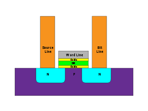
with the addition of a small sliver of silicon nitride inserted inside the transistor's gate oxide. The sliver of nitride is non-conductive but contains a large number of charge trapping sites able to hold an electrostatic charge. The nitride layer is electrically isolated from the surrounding transistor, although charges stored on the nitride directly affect the conductivity of the underlying transistor channel. The oxide/nitride sandwich typically consists of a 2 nm thick oxide lower layer, a 5 nm thick silicon nitride middle layer, and a 5—10 nm oxide upper layer.
When the polysilicon control gate is biased positively, electrons from the transistor source and drain regions tunnel
through the oxide layer and get trapped in the silicon nitride. This results in an energy barrier between the drain and the source, raising the threshold voltage
Vt (the gate-source voltage necessary for current to flow through the transistor). The electrons can be removed again by applying a negative bias on the control gate.
A SONOS memory array is constructed by fabricating a grid of SONOS transistors which are connected by horizontal and vertical control lines (wordlines and bitlines) to peripheral circuitry such as address decoder
s and sense amplifiers. After storing or erasing the cell, the controller can measure the state of the cell by passing a small voltage across the source-drain nodes; if current flows the cell must be in the "no trapped electrons" state, which is considered a logical
"0". If no current is seen the cell is in the "1" state. The needed voltages are normally about 2 V for the erased state, and around 4.5 V for the programmed state.
Additionally, traditional flash is less tolerant of oxide defects because a single shorting defect will discharge the entire polysilicon floating gate. The nitride in the SONOS structure is non-conductive, so a short only disturbs a localized patch of charge. Even with the introduction of new insulator technologies this has a definite "lower limit" around 7 to 12 nm, which means it is difficult for flash devices to scale smaller than about 45 nm linewidths. SONOS, on the other hand, requires a very thin layer of insulator in order to work, making the gate area smaller than flash. This allows SONOS to scale to smaller linewidth, with recent examples being produced on 40 nm fabs and claims that it will scale to 20 nm. The linewidth is directly related to the overall storage of the resulting device, and indirectly related to the cost; in theory, SONOS' better scalability will result in higher capacity devices at lower costs.
Additionally, the voltage needed to bias the gate during writing is much smaller than in traditional flash. In order to write flash, power is first built up in a separate device known as a charge pump
, which multiplies the input voltage to between 9 V to 20 V. This process takes some time, meaning that writing to a flash cell is much slower than reading, often between 100 and 1000 times slower. The pulse of high power also degrades the cells slightly, meaning that flash devices can only be written to between 10,000 and 100,000 times, depending on the type. SONOS devices require much lower write voltages, typically 5—8 V, and do not degrade in the same way. SONOS does suffer from an unrelated problem, however, where electrons become strongly trapped in the ONO layer and cannot be removed again. Over long usage this can eventually lead to enough trapped electrons to permanently set the cell to the "1" state, similar to the problems in flash. However, in SONOS this requires on the order of a 100,000,000 write cycles, 1000 to 10,000 times better than flash.
were demonstrating program/erase voltages in the range of 5—12 volts.
is one of the groups working on SONOS devices, and have produced small 26-bit demonstrators with excellent lifetimes at a 120 nm linewidth. It is not clear if this research is ongoing, however, given the rapid advances in flash technology that have led to very large gains in areal density. Other groups are also working on SONOS for more specialized tasks, notably military and space systems due to its excellent radiation hardness.
Spansion
recently announced the development of SONOS flash memory using its MirrorBit technology. Infineon
and later its spin-off Qimonda
also produced SONOS flash memories.
Non-volatile memory
Non-volatile memory, nonvolatile memory, NVM or non-volatile storage, in the most basic sense, is computer memory that can retain the stored information even when not powered. Examples of non-volatile memory include read-only memory, flash memory, ferroelectric RAM, most types of magnetic computer...
computer memory
Computer memory
In computing, memory refers to the physical devices used to store programs or data on a temporary or permanent basis for use in a computer or other digital electronic device. The term primary memory is used for the information in physical systems which are fast In computing, memory refers to the...
closely related to Flash RAM. It is distinguished from mainstream flash by the use of silicon nitride
Silicon nitride
Silicon nitride is a chemical compound of silicon and nitrogen. If powdered silicon is heated between 1300° and 1400°C in an atmosphere of nitrogen, trisilicon tetranitride, Si3N4, is formed. The silicon sample weight increases progressively due to the chemical combination of silicon and nitrogen...
(Si3N4) instead of polysilicon for the charge storage material. A further variant is "SHINOS" ("Silicon Hi-k
High-k Dielectric
The term high-κ dielectric refers to a material with a high dielectric constant κ used in semiconductor manufacturing processes which replaces the silicon dioxide gate dielectric...
Nitride Oxide Silicon"). SONOS promises lower programming voltages and higher program/erase cycle endurance than polysilicon-based flash, and is an area of active research and development effort. Companies offering SONOS-based products include GlobalFoundries
GLOBALFOUNDRIES
GlobalFoundries Inc. is the world's third largest independent semiconductor foundry, with its headquarters located in Milpitas, California. GlobalFoundries was created by the divestiture of the manufacturing side of AMD on March 2, 2009, and was expanded through its merger with Chartered...
, Cypress Semiconductor
Cypress Semiconductor
Cypress Semiconductor Corporation is a Silicon Valley-based semiconductor design and manufacturing company founded by T. J. Rodgers and others from Advanced Micro Devices. It was formed in 1982 with backing by Sevin Rosen and went public in 1986. The company initially focused on the design and...
, Macronix, Toshiba
Toshiba
is a multinational electronics and electrical equipment corporation headquartered in Tokyo, Japan. It is a diversified manufacturer and marketer of electrical products, spanning information & communications equipment and systems, Internet-based solutions and services, electronic components and...
, and United Microelectronics Corporation
United Microelectronics Corporation
UMC was founded as Taiwan's first semiconductor company in 1980 as a spin-off of the government-sponsored Industrial Technology Research Institute .-Overview:...
.
Description
Memory cell
Memory cell may refer to:* Memory cell, a building block of computer data storage*Memory B cell, an antibody producing cell*Memory T cell, an infection fighting cell...
is formed from a standard polysilicon N-channel MOSFET
MOSFET
The metal–oxide–semiconductor field-effect transistor is a transistor used for amplifying or switching electronic signals. The basic principle of this kind of transistor was first patented by Julius Edgar Lilienfeld in 1925...
transistor
Transistor
A transistor is a semiconductor device used to amplify and switch electronic signals and power. It is composed of a semiconductor material with at least three terminals for connection to an external circuit. A voltage or current applied to one pair of the transistor's terminals changes the current...
with the addition of a small sliver of silicon nitride inserted inside the transistor's gate oxide. The sliver of nitride is non-conductive but contains a large number of charge trapping sites able to hold an electrostatic charge. The nitride layer is electrically isolated from the surrounding transistor, although charges stored on the nitride directly affect the conductivity of the underlying transistor channel. The oxide/nitride sandwich typically consists of a 2 nm thick oxide lower layer, a 5 nm thick silicon nitride middle layer, and a 5—10 nm oxide upper layer.
When the polysilicon control gate is biased positively, electrons from the transistor source and drain regions tunnel
Quantum tunnelling
Quantum tunnelling refers to the quantum mechanical phenomenon where a particle tunnels through a barrier that it classically could not surmount. This plays an essential role in several physical phenomena, such as the nuclear fusion that occurs in main sequence stars like the sun, and has important...
through the oxide layer and get trapped in the silicon nitride. This results in an energy barrier between the drain and the source, raising the threshold voltage
Threshold voltage
The threshold voltage of a MOSFET is usually defined as the gate voltage where an inversion layer forms at the interface between the insulating layer and the substrate of the transistor. The purpose of the inversion layer's forming is to allow the flow of electrons through the gate-source junction...
Vt (the gate-source voltage necessary for current to flow through the transistor). The electrons can be removed again by applying a negative bias on the control gate.
A SONOS memory array is constructed by fabricating a grid of SONOS transistors which are connected by horizontal and vertical control lines (wordlines and bitlines) to peripheral circuitry such as address decoder
Address decoder
In digital electronics, an address decoder is a decoder circuit that has two or more bits of an address bus as inputs and that has one or more device selection lines as outputs. When the address for a particular device appears on the address bus, the address decoder asserts the selection line for...
s and sense amplifiers. After storing or erasing the cell, the controller can measure the state of the cell by passing a small voltage across the source-drain nodes; if current flows the cell must be in the "no trapped electrons" state, which is considered a logical
Boolean logic
Boolean algebra is a logical calculus of truth values, developed by George Boole in the 1840s. It resembles the algebra of real numbers, but with the numeric operations of multiplication xy, addition x + y, and negation −x replaced by the respective logical operations of...
"0". If no current is seen the cell is in the "1" state. The needed voltages are normally about 2 V for the erased state, and around 4.5 V for the programmed state.
Comparison with standard flash
Generally SONOS is very similar to standard double polysilicon flash, but hypothetically offers higher quality storage. This is due to the smooth homogeneity of the Si3N4 film compared with polycrystalline film which has tiny irregularities. Flash requires the construction of a very high-performance insulating barrier on the gate leads of its transistors, often requiring as many as nine different steps, whereas the oxide layering in SONOS can be more easily produced on existing lines and more easily combined with CMOS logic.Additionally, traditional flash is less tolerant of oxide defects because a single shorting defect will discharge the entire polysilicon floating gate. The nitride in the SONOS structure is non-conductive, so a short only disturbs a localized patch of charge. Even with the introduction of new insulator technologies this has a definite "lower limit" around 7 to 12 nm, which means it is difficult for flash devices to scale smaller than about 45 nm linewidths. SONOS, on the other hand, requires a very thin layer of insulator in order to work, making the gate area smaller than flash. This allows SONOS to scale to smaller linewidth, with recent examples being produced on 40 nm fabs and claims that it will scale to 20 nm. The linewidth is directly related to the overall storage of the resulting device, and indirectly related to the cost; in theory, SONOS' better scalability will result in higher capacity devices at lower costs.
Additionally, the voltage needed to bias the gate during writing is much smaller than in traditional flash. In order to write flash, power is first built up in a separate device known as a charge pump
Charge pump
A charge pump is a kind of DC to DC converter that uses capacitors as energy storage elements to create either a higher or lower voltage power source. Charge pump circuits are capable of high efficiencies, sometimes as high as 90–95% while being electrically simple circuits.Charge pumps use some...
, which multiplies the input voltage to between 9 V to 20 V. This process takes some time, meaning that writing to a flash cell is much slower than reading, often between 100 and 1000 times slower. The pulse of high power also degrades the cells slightly, meaning that flash devices can only be written to between 10,000 and 100,000 times, depending on the type. SONOS devices require much lower write voltages, typically 5—8 V, and do not degrade in the same way. SONOS does suffer from an unrelated problem, however, where electrons become strongly trapped in the ONO layer and cannot be removed again. Over long usage this can eventually lead to enough trapped electrons to permanently set the cell to the "1" state, similar to the problems in flash. However, in SONOS this requires on the order of a 100,000,000 write cycles, 1000 to 10,000 times better than flash.
History
SONOS was first conceptualized in the 1960s. In the early 1970s initial commercial devices were realized using PMOS transistors and a metal-nitride-oxide (MNOS) stack with a 45 nm nitride storage layer. These devices required up to 30V to operate. By the early 1980s, polysilicon NMOS-based structures were in use with operating voltages under 20 V. By the late 1980s and early 1990s PMOS SONOS structureswere demonstrating program/erase voltages in the range of 5—12 volts.
Current efforts
PhilipsPhilips
Koninklijke Philips Electronics N.V. , more commonly known as Philips, is a multinational Dutch electronics company....
is one of the groups working on SONOS devices, and have produced small 26-bit demonstrators with excellent lifetimes at a 120 nm linewidth. It is not clear if this research is ongoing, however, given the rapid advances in flash technology that have led to very large gains in areal density. Other groups are also working on SONOS for more specialized tasks, notably military and space systems due to its excellent radiation hardness.
Spansion
Spansion
Spansion Inc. is a Flash memory chip maker that designs, develops and manufactures NOR flash memory products. The company has over 3,400 employees and is headquartered in Sunnyvale, California. Spansion is a former joint-venture between AMD and Fujitsu....
recently announced the development of SONOS flash memory using its MirrorBit technology. Infineon
Infineon Technologies
Infineon Technologies AG is a German semiconductor manufacturer and was founded on April 1, 1999, when the semiconductor operations of the parent company Siemens AG were spun off to form a separate legal entity. , Infineon has 25,149 employees worldwide...
and later its spin-off Qimonda
Qimonda
Qimonda AG, was a memory company split out of Infineon Technologies on 1 May 2006, to form at the time the second largest DRAM company worldwide, according to the industry research firm Gartner Dataquest...
also produced SONOS flash memories.