

Nantenna
Encyclopedia
Nanoscopic scale
The nanoscopic scale usually refers to structures with a length scale applicable to nanotechnology, usually cited as 1-100 nanometers. The nanoscopic scale is a lower bound to the mesoscopic scale for most solids....
rectifying antenna
Rectenna
A rectenna is a rectifying antenna, a special type of antenna that is used to directly convert microwave energy into DC electricity. Its elements are usually arranged in a multi element phased array with a mesh pattern reflector element to make it directional...
. Nantennas may prove useful for converting solar radiation to electricity, an idea first proposed by Robert L. Bailey in 1972.. As of June 2011, nantenna devices are not yet commercially available, and it is unknown if they will ever be as cost-effective as photovoltaic cells.
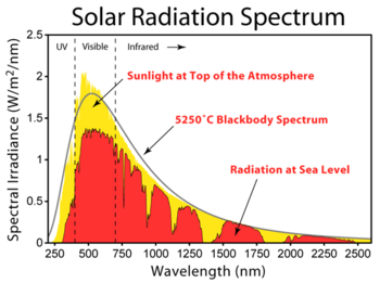
A nantenna is an electromagnetic collector designed to absorb specific wavelengths that are proportional to the size of the nantenna. Currently, Idaho National Laboratories has designed a nantenna to absorb wavelengths in the range of 3–15 μm. These wavelengths correspond to photon energies of . Based on antenna theory, a nantenna can absorb any wavelength of light efficiently provided that the size of the nantenna is optimized for that specific wavelength. Ideally, nantennas would be used to absorb light at wavelengths between because these wavelengths have higher energy than far-infrared (longer wavelengths) and make up about 85% of the solar radiation spectrum (see Figure 1).
{| align=""
| |}
History of nantennas
Robert Bailey, along with James C. Fletcher, received a patent in 1973 for an “electromagnetic wave converter”. The patented device was similar to modern day nantenna devices. Alvin M. Marks received a patent in 1984 for a device explicitly stating the use of sub-micron antennas for the direct conversion of light power to electrical power. Marks’s device showed substantial improvements in efficiency over Bailey’s device.In 1996, Guang H. Lin was the first to report resonant light absorption by a fabricated nanostructure and rectification of light with frequencies in the visible range. In 2002, ITN Energy Systems, Inc. published a report on their work on optical antennas coupled with high frequency diode
Diode
In electronics, a diode is a type of two-terminal electronic component with a nonlinear current–voltage characteristic. A semiconductor diode, the most common type today, is a crystalline piece of semiconductor material connected to two electrical terminals...
s. ITN set out to build a nantenna array with single digit efficiency. Although they were unsuccessful, the issues associated with building a high efficiency nantenna were better understood. Research on nantennas is ongoing.
Theory of nantennas
The theory behind nantennas is essentially the same for rectifying antennasRectenna
A rectenna is a rectifying antenna, a special type of antenna that is used to directly convert microwave energy into DC electricity. Its elements are usually arranged in a multi element phased array with a mesh pattern reflector element to make it directional...
. Incident light on the antenna causes electrons in the antenna to move back and forth at the same frequency as the incoming light. This is caused by the oscillating electric field of the incoming electromagnetic wave. The movement of electrons is an alternating current in the antenna circuit. To convert this into direct current
Direct current
Direct current is the unidirectional flow of electric charge. Direct current is produced by such sources as batteries, thermocouples, solar cells, and commutator-type electric machines of the dynamo type. Direct current may flow in a conductor such as a wire, but can also flow through...
, the AC
Alternating current
In alternating current the movement of electric charge periodically reverses direction. In direct current , the flow of electric charge is only in one direction....
must be rectified, which is typically done with some kind of diode
Diode
In electronics, a diode is a type of two-terminal electronic component with a nonlinear current–voltage characteristic. A semiconductor diode, the most common type today, is a crystalline piece of semiconductor material connected to two electrical terminals...
. The resulting DC current can then be used to power an external load.
The resonant frequency of antennas (frequency which results in lowest impedance and thus highest efficiency) scales linearly with the physical dimensions of the antenna according to simple microwave antenna theory. The wavelengths in the solar spectrum range from approximately 0.3-2.0 μm. Thus, in order for a rectifying antenna to be an efficient electromagnetic collector in the solar spectrum, it needs to be on the order of hundreds of nm in size.
Skin effect
Skin effect is the tendency of an alternating electric current to distribute itself within a conductor with the current density being largest near the surface of the conductor, decreasing at greater depths. In other words, the electric current flows mainly at the "skin" of the conductor, at an...
”. From a purely device perspective, the I-V characteristics would appear to no longer be ohmic, even though Ohm’s law is still valid.
Another complication of scaling down is that diode
Diode
In electronics, a diode is a type of two-terminal electronic component with a nonlinear current–voltage characteristic. A semiconductor diode, the most common type today, is a crystalline piece of semiconductor material connected to two electrical terminals...
s used in larger scale rectennas cannot operate at THz frequencies without large loss in power. The large loss in power is a result of the junction capacitance (also known as parasitic capacitance) found in p-n junction diodes and Schottky diodes, which can only operate effectively at frequencies less than 5 THz. The ideal wavelengths of 0.4–1.6 μm correspond to frequencies of approximately 190–750 THz, which is much larger than the capabilities of typical diodes. Therefore, alternative diodes need to be used for efficient power conversion. In current nantenna devices, metal-insulator-metal (MIM) tunneling diodes are used. Unlike Schottky diodes, MIM diodes are not affected by parasitic capacitances because they work on the basis of electron tunneling. Because of this, MIM diodes have been shown to operate effectively at frequencies around 150 THz.
Advantages of nantennas
One of the biggest claimed advantages of nantennas is their high theoretical efficiency. When compared to the theoretical efficiency of single junction solar cells (30%), nantennas appear to have a significant advantage. However, the two efficiencies are calculated using different assumptions.The assumptions involved in the nantenna calculation are based on the application of the Carnot efficiency of solar collectors. The Carnot efficiency, η, is given by
where Tcold is the temperature of the cooler body and Thot is the temperature of the warmer body. In order for there to be an efficient energy conversion, the temperature difference between the two bodies must be significant. R. L. Bailey claims that nantennas are not limited by Carnot efficiency, whereas photovoltaics
Photovoltaics
Photovoltaics is a method of generating electrical power by converting solar radiation into direct current electricity using semiconductors that exhibit the photovoltaic effect. Photovoltaic power generation employs solar panels composed of a number of solar cells containing a photovoltaic material...
are. However, he does not provide any argument for this claim. Furthermore, when the same assumptions used to obtain the 85% theoretical efficiency for nantennas are applied to single junction solar cells, the theoretical efficiency of single junction solar cells is also greater than 85%.
The most apparent advantage nantennas have over semiconductor photovoltaics is that nantenna arrays can be designed to absorb any frequency of light. The resonant frequency of a nantenna can be selected by varying its length. This is an advantage over semiconductor photovoltaics, because in order to absorb different wavelengths of light, different band gaps are needed. In order to vary the band gap, the semiconductor must be alloyed or a different semiconductor must be used altogether.
Limitations and disadvantages of nantennas
As previously stated, one of the major limitations of nantennas is the frequency at which they operate. The high frequency of light in the ideal range of wavelengths makes the use of typical Schottky diodes impractical. Although MIM diodes show promising features for use in nantennas, more advances are necessary to operate efficiently at higher frequencies.Another disadvantage is that current nantennas are produced using electron beam (e-beam
Electron beam processing
Electron beam processing or electron irradiation is a process which involves using electrons, usually of high energy, to treat an object for a variety of purposes. This may take place under elevated temperatures and nitrogen atmosphere...
) lithography. This process is slow and relatively expensive because parallel processing is not possible with e-beam lithography. Typically, e-beam lithography is only used for research purposes when extremely fine resolutions are needed for minimum feature size (typically, on the order of nanometers). However, photolithographic techniques have advanced to where it is possible to have minimum feature sizes on the order of tens of nanometers, making it possible to produce nantennas by means of photolithography.
Production of a nantenna
After the proof of concept was completed, laboratory-scale silicon wafers were fabricated using standard semiconductor integrated circuit fabrication techniques. E-beam lithography was used to fabricate the arrays of loop antenna metallic structures. The nantenna consists of three main parts: the ground plane, the optical resonance cavity, and the antenna. The antenna absorbs the electromagnetic wave, the ground plane acts to reflect the light back towards the antenna, and the optical resonance cavity bends and concentrates the light back towards the antenna via the ground plane.Lithography method
Idaho National Labs used the following steps to fabricate their nantenna arrays. A metallic ground plane was deposited on a bare silicon wafer, followed by a sputter deposited amorphous silicon layer. The depth of the deposited layer was about a quarter of a wavelength. A thin manganese film along with a gold frequency selective surface (to filter wanted frequency) was deposited to act as the antenna. Resist was applied and patterned via electron beam lithography. The gold film was selectively etched and the resist was removed.Roll-to-roll manufacturing
In moving up to a greater production scale, laboratory processing steps such as the use of e-beam lithography are slow and expensive. Therefore a roll-to-roll manufacturingRoll-to-roll processing
In the field of electronic devices, Roll-to-roll processing, also known as web processing, reel-to-reel processing or R2R, is the process of creating electronic devices on a roll of flexible plastic or metal foil...
method was devised using a new manufacturing technique based on a master pattern. This master pattern in effect mechanically “stamps” the precision pattern onto an inexpensive flexible substrate and thereby creates the metallic loop elements seen in the laboratory processing steps. The master template fabricated by Idaho National Laboratories consists of approximately 10 billion antenna elements on an 8-inch round silicon wafer. Using this semi-automated process, Idaho National Labs has produced a number of 4-inch square coupons. These coupons were combined to form a broad flexible sheet of nantenna arrays.
Proof of principle
The proof of principle for nantennas started out with a 1 cm2 silicon substrate with the printed nantenna array filling the area. The device was tested using infrared light with a range of 3 to 15 microns. The peak emissivity is found to be centered at 6.5 microns and reaches an emissivity of 1. An emissivity of 1 means the nantenna absorbs all of the photons of a specific wavelength (in this case, 6.5 microns) that are incident upon the device. Comparing the experimental spectrum to the modeled spectrum, the experimental results are in agreement with theoretical expectations (Figure 5). In some areas, the nantenna had a lower emissivity than the theoretical expectations, but in other areas, namely at around 3.5 microns, the device absorbed more light than expected.
Economics of nantennas
Nantennas are cheaper than photovoltaics. While materials and processing of photovoltaics are dear (currently the cost for complete photovoltaic modules is in the order of and declining.), Steven Novack estimates the current cost of the nantenna material itself as around . With proper processing techniques and different material selection, he estimates that the overall cost of processing, once properly scaled up, will not cost much more. His prototype was a of plastic, which contained only of goldGold
Gold is a chemical element with the symbol Au and an atomic number of 79. Gold is a dense, soft, shiny, malleable and ductile metal. Pure gold has a bright yellow color and luster traditionally considered attractive, which it maintains without oxidizing in air or water. Chemically, gold is a...
, with the possibility of downgrading to a material such as aluminum, copper
Copper
Copper is a chemical element with the symbol Cu and atomic number 29. It is a ductile metal with very high thermal and electrical conductivity. Pure copper is soft and malleable; an exposed surface has a reddish-orange tarnish...
, or silver
Silver
Silver is a metallic chemical element with the chemical symbol Ag and atomic number 47. A soft, white, lustrous transition metal, it has the highest electrical conductivity of any element and the highest thermal conductivity of any metal...
. The prototype used a silicon substrate due to familiar processing techniques, but any substrate could theoretically be used as long as the ground plane material adheres properly.
Future research and goals
In an interview on National Public Radio's Talk of the Nation, Dr. Novak claimed that nantennas could one day be used to power cars, charge cell phones, and even cool homes. Novak claims the last of these will work by both absorbing the infrared heat available in the room and producing electricity which could be used to further cool the room.Currently, the largest problem is not with the antenna device, but with the rectifier. As previously stated, present-day diodes are unable to efficiently rectify at frequencies which correspond to high-infrared and visible light. Therefore, a rectifier must be designed that can properly turn the absorbed light into usable energy. Researchers currently hope to create a rectifier which can convert around 50% of the antenna's absorption into energy.
Another focus of research will be how to properly upscale the process to mass-market production. New materials will need to be chosen and tested that will easily comply with a roll-to-roll manufacturing process.