

Multijunction photovoltaic cell
Encyclopedia
Multi-junction solar cells or tandem cells are solar cell
s containing several p-n junction
s. Each junction is tuned to a different wavelength of light
, reducing one of the largest inherent sources of losses, and thereby increasing efficiency. Traditional single-junction cells have a maximum theoretical efficiency of 34%, a theoretical "infinite-junction" cell would improve this to 87% under highly concentrated sunlight.
Currently, the best lab examples of traditional silicon solar cells have efficiencies around 25%, while lab examples of multi-junction cells have demonstrated performance over 42%. Commercial examples of tandem cells are widely available at 30% under one-sun illumination, and improve to around 40% under concentrated sunlight. However, this efficiency is gained at the cost of increased complexity and manufacturing price. To date, their higher price and lower price-to-performance ratio have limited their use to special roles, notably in aerospace
where their high power-to-weight ratio
is desirable. In terrestrial applications these solar cells are used in concentrated photovoltaics
(CPV) with operating plants all over the world .
Tandem techniques can also be used to improve the performance of existing cell designs, although there are strict limits in the choice of materials. In particular, the technique can be applied to thin-film solar cells using amorphous silicon
to produce a cell with about 10% efficiency that is lightweight and flexible. This approach has been used by several commercial vendors, but these products are currently limited to certain niche roles, like roofing materials.
silicon
and then depositing metallic contacts on the top and bottom. The doping is normally applied to a thin layer on the top of the cell, producing a pn-junction with a particular bandgap energy, Eg.
Photon
s that hit the top of the solar cell are either reflected or transmitted. Transmitted photons have the potential to give their energy hν to an electron
if hν ≥ Eg, generating an electron-hole
pair. In the depletion region, the drift electric field Edrift accelerates both electrons and holes towards their respective n-doped and p-doped regions (up and down, respectively). The resulting current
Ig is called the generation photocurrent
. In the quasi-neutral region, the scattering electric field Escatt accelerates holes (electrons) towards the p-doped (n-doped) region, which gives a scattering photocurrent Ipscatt (Inscatt). Consequently, due to the accumulation of charge
s, a potential V and a photocurrent Iph appear. The expression for this photocurrent is obtained by adding generation and scattering photocurrents: Iph = Ig + Inscatt + Ipscatt.
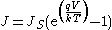
The J-V characteristics (J is current density, i.e. current per unit area) of a solar cell under illumination are simply obtained by shifting the J-V characteristics of a diode
in the dark downward by Iph, as shown in Figure B. Since solar cells are designed to supply power and not absorb it, the power P = V·Iph must be negative. Hence, the operating point (Vm, Jm) is located in the region where V>0 and Iph<0, and chosen to maximize the absolute value
of the power |P|.
The first are the losses due to blackbody radiation, a loss mechanism that affects any material object above absolute zero
. In the case of solar cells at standard temperature and pressure, this loss accounts for about 7% of the power. The second is an effect known as "recombination", where the electron
s created by the photoelectric effect
meet the electron hole
s left behind by previous excitations. In silicon, this accounts for another 10% of the power.
However, the dominant loss mechanism is the inability for a solar cell to extract all of the power in the photon
, and the associated problem that it cannot extract any power at all from certain photons. This is due to the fact that the electrons have to gain enough energy to overcome the bandgap of the material, and that energy is removed from the energy originally in the photon.
If the photon has less energy than the bandgap, it is not collected at all. This is a major consideration for conventional solar cells, which are not sensitive to most of the infrared
spectrum, although that represents almost half of the power coming from the sun. Conversely, photons with more energy than the bandgap, say blue light, initially eject a photon with much more energy than the bandgap, but this extra energy is lost through a process known as "relaxation". This lost energy turns into heat in the cell, which has the side-effect of further increasing blackbody losses.
This results in a catch-22
situation. If one decreases the bandbap energy in order to capture more photons, more energy is lost from the shorter wavelength light. If one instead increases the bandgap in order to capture more energy from shorter wavelengths, more photons fail to be captured. Carrying out the analysis for the AM1.5 spectrum, the perfect balance is reached at about 1.1 eV, the near infrared, which happens to be very close to the natural bandgap in silicon and a number of other useful semiconductors.
Combining all of these factors, the maximum efficiency for a single-bandgap material, like conventional silicon cells, is about 34%. That is, 66% of the energy in the sunlight hitting the cell will be lost. Practical concerns further reduce this, notably reflection off the front surface or the metal terminals, with modern high-quality cells at about 22%.
For instance, if one had a cell with two bandgaps in it, one tuned to red light and the other to green, then the extra energy in green, cyan and blue light would be lost only to the bandgap of the green-sensitive material, while the energy of the red, yellow and orange would be lost only to the bandgap of the red-sensitive material. Following analysis similar to those performed for single-bandgap devices, it can be demonstrated that the perfect bandgaps for a two-gap device is at 1.1 eV and 1.8 eV.
Conveniently, light of a particular wavelength does not interact strongly with materials that are not a multiple of that wavelength. This means that you can make a multijunction cell by layering the different materials on top of each other, shortest wavelengths on the "top" and increasing through the body of the cell. As the photons have to pass through the cell to reach the proper layer to be absorbed, transparent conductors
need to be used to collect the electrons being generated at each layer.
s and then wire them together separately outside the cell. This technique is widely used by amorphous silicon
solar cells, Uni-Solar's products use three such layers to reach efficiencies around 9%. Lab examples using more exotic thin-film materials have demonstrated efficiencies over 30%.
The more difficult solution is the "monolithically integrated" cell, where the cell consists of a number of layers that are mechanically and electrically connected. These cells are much more difficult to produce because the electrical characteristics of each layer has to be carefully matched. In particular, the photocurrent generated in each layer needs to be matched, otherwise electrons will be absorbed between layers. This limits their construction to certain materials, best met by the III-V semiconductors.
For optimal growth and resulting crystal quality, the crystal lattice constant a of each material must be closely matched, resulting in lattice-matched devices. This constraint has been relaxed somewhat in recently-developed metamorphic solar cells which contain a small degree of lattice mismatch. However, a greater degree of mismatch or other growth imperfections can lead to crystal defects causing a degradation in electronic properties.
Since each sub-cell is connected electrical in series, the same current flows through each junction. The materials are ordered with decreasing bandgaps, Eg, allowing sub-bandgap light (hc/λ < e·Eg) to transmit to the lower sub-cells. Therefore, suitable bandgaps must be chosen such that the design spectrum will balance the current generation in each of the sub-cells, achieving current matching. Figure C(b) plots spectral irradiance E(λ), which is the source power density at a given wavelength
λ. It is plotted together with the maximum conversion efficiency for every junction as a function of the wavelength, which is directly related to the number of photons available for conversion into photocurrent.
Finally, the layers must be electrically optimal for high performance. This necessitates usage of materials with strong absorption coefficients α(λ), high minority carrier lifetimes τminority, and high mobilities µ.
The favorable values in the table below justify the choice of materials typically used for multi-junction solar cells: InGaP for the top sub-cell (Eg = 1.8 - 1.9 eV), InGaAs for the middle sub-cell (Eg = 1.4 eV), and Germanium
for the bottom sub-cell (Eg = 0.67 eV). The use of Ge is mainly due to its lattice constant, robustness, low cost, abundance, and ease of production.
Because the different layers are closely lattice-matched, the fabrication of the device typically employs metal-organic chemical vapor deposition
(MOCVD). This technique is preferable to the molecular beam epitaxy
(MBE) because it ensures high crystal
quality and large scale production.
are low-resistivity electrodes that make contact with the semiconductor layer in GaAs. They are positioned on the two sides of the structure but mainly on the backwards face so that shadowing on the lightning surface is reduced.
(AR) coating is generally composed of several layers in the case of MJ solar cells. The top AR layer has usually a NaOH surface texturation with several pyramid
s in order to increase the transmission coefficient T, the trapping of the light in the material (because photons cannot easily get out the MJ structure due to pyramids) and therefore, the path length of photons in the material. On the one hand, the thickness of each AR layer is chosen to get destructive interferences. Therefore, the reflection coefficient R decreases to 1%. In the case of two AR layers L1 (the top layer, usually ) and L2 (usually ), there must be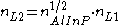 to have the same amplitudes for reflected fields and nL1dL1 = 4λmin,nL2dL2 = λmin/4 to have opposite phase for reflected fields. On the other hand, the thickness of each AR layer is also chosen to minimize the reflectance at wavelengths for which the photocurrent is the lowest. Consequently, this maximizes JSC by matching currents of the three subcells.As example, because the current generated by the bottom cell is greater than the currents generated by the other cells, the thickness of AR layers is adjusted so that the infrared (IR) transmission (which corresponds to the bottom cell) is degraded while the ultraviolet
transmission (which corresponds to the top cell) is upgraded. Particularly, an AR coating is very important at low wavelengths because, without it, T would be strongly reduced to 70%.
s is to provide a low electrical resistance
and optically low-loss connection between two subcells. Without it, the p-doped region of the top cell would be directly connected with the n-doped region of the middle cell. Hence, a pn junction with opposite direction to the others would appear between the top cell and the middle cell. Consequently, the photovoltage
would be lower than if there would be no parasitic diode
. In order to decrease this effect, a tunnel junction is used. It is simply a wide band gap, highly doped diode. The high doping reduces the length of the depletion region because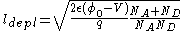
Hence, electrons can easily tunnel through the depletion region. The J-V characteristic of the tunnel junction is very important because it explains why tunnel junctions can be used to have a low electrical resistance connection between two pn junctions. Figure D shows three different regions: the tunneling region, the negative differential resistance region and the thermal diffusion region. The region where electrons can tunnel through the barrier is called the tunneling region. There, the voltage must be low enough so that energy of some electrons who are tunneling is equal to energy states available on the other side of the barrier. Consequently, current density through the tunnel junction is high (with maximum value of , the peak current density) and the slope near the origin is therefore steep. Then, the resistance is extremely low and consequently, the voltage
too.. This is why tunnel junctions are ideal for connecting two pn junctions without having a voltage drop. When voltage is higher, electrons cannot cross the barrier because energy states are no longer available for electrons. Therefore, the current density decreases and the differential resistance is negative. The last region, called thermal diffusion region, corresponds to the J-V characteristic of the usual diode:
In order to avoid the reduction of the MJ solar cell performances, tunnel junctions must be transparent to wavelengths absorbed by the next photovoltaic cell, the middle cell, i.e. EgTunnel > EgMiddleCell.
which catches electrons (holes). Indeed, despite the electric field
Ed, these cannot jump above the barrier formed by the heterojunction because they don't have enough energy, as illustrated in figure E. Hence, electrons (holes) cannot recombine with holes (electrons) and cannot diffuse through the barrier. By the way, window and BSF layers must be transparent to wavelengths absorbed by the next pn junction i.e. EgWindow > EgEmitter and EgBSF > EgEmitter. Furthermore, the lattice constant must be close to the one of InGaP and the layer must be highly doped (n ≥ 1018 cm−3).
Because of the impossibility to obtain JSC1, JSC2, JSC3 directly from the total J-V characteristic, the quantum efficiency QE(λ) is utilized. It measures the ratio between the amount of electron-hole pairs created and the incident photons at a given wavelength λ. Let φi(λ) be the photon flux of corresponding incident light in subcell iandQEi(λ) be the quantum efficiency of the subcell i. By definition, this equates to: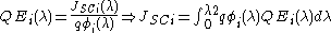
The value of is obtained by linking it with the absorption coefficient
 , i.e. the number of photons absorbed per unit of length by a material. If it is assumed that each photon absorbed by a subcell creates an electron/hole pair (which is a good approximation), this leads to :
 where di is the thickness of the subcell i and
  is the percentage of incident light which is not absorbed by the subcell i.
Similarly, because , the following approximation can be used:
 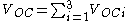 .
.
The values of are then given by the J-V diode equation:
in the range In.5Ga.5P through In.53Ga.47P serve as the high band gap alloy. This alloy range provides for the ability to have band gaps in the range of 1.92eV to 1.87eV. The lower GaAs
junction has a band gap of 1.42eV.
, Gallium arsenide or Indium gallium arsenide
and Germanium
can be fabricated on germanium wafers. Early cells used straight gallium arsenide in the middle junction. Later cells have utilized In0.015Ga0.985As, due to the better lattice match to Ge, resulting in a lower defect density.
Due to the huge band gap difference between GaAs (1.42eV), and Ge (0.66eV), the current match is very poor, with the Ge junction operated significantly current limited.
Current efficiencies for InGaP/GaAs/Ge cells are in the mid 30% range. Lab cells using additional junctions between the GaAs and Ge junction have demonstrated efficiencies above 40%.
(In0.53Ga0.47As) is lattice matched to Indium Phosphide with a band gap of 0.74eV. A quaternary alloy of Indium gallium arsenide phosphide can be lattice matched for any band gap in between the two.
Indium phosphide-based cells have the potential to work in tandem with gallium arsenide cells. The two cells can be optically connected in series (with the InP cell below the GaAs cell), or in parallel through the use of spectra splitting using a Dichroic filter
.
GaAsSb heterojunction tunnel diodes offer other advantages. The same current can be achieved by using a lower doping. Secondly, because the lattice constant is larger for GaAsSb than Ge, one can use a wider range of materials for the bottom cell because more materials are lattice-matched to GaAsSb than to Ge.
Chemical components can be added to some layers. Adding about one percent of Indium
in each layer better matches lattice constants of the different layers. Without it, there is about 0.08 percent of mismatching between layers, which inhibits performance. Adding aluminium to the top cell increases its band gap to 1.96 eV, covering a larger part of the solar spectrum and obtain a higher open-circuit voltage VOC.
The theoretical efficiency of MJ solar cells is 86.8% for an infinite number of pn junctions, implying that more junctions increase efficiency. The maximum theoretical efficiency is 37, 50, 56, 72% for 1, 2, 3, 36 pn junctions, respectively, with the number of junctions increasing exponentially to achieve equal effiency increments. The exponential relationship implies that as the cell approaches the limit of efficiency, the increase cost and complexity grow rapidly. Decreasing the thickness of the top cell increases the transmission coefficient T.
Finally, an InGaP hetero-layer between the p-Ge layer and the InGaAs layer can be added in order to create automatically the n-Ge layer by scattering during MOCVD growth and increase significantly the quantum efficiency QE(λ) of the bottom cell. InGaP is advantageous because of its high scattering coefficient and low solubility in Ge.
es and reflective dishes. Thanks to these devices, light arriving on a large surface can be concentrated on a smaller cell. The intensity concentration ratio (or “suns”) is the average intensity of the focused light divided by 0.1 W/m². If its value is X then the MJ current becomes X higher under concentrated illumination.
Using concentrations on the order of 500 to 1000, meaning that a 1 cm² cell can use the light collected from 0.1 m² (as 1 m2 equal 10000 cm2), produces the highest efficiencies seen to date. Three-layer cells are fundamentally limited to 63%, but existing commercial prototypes have already demonstrated over 40%. These cells capture about 2/3 of their theoretical maximum performance, so assuming the same is true for a non-concentrated version of the same design, one might expect a three-layer cell of 30% efficiency. This is not enough of an advantage over traditional silicon designs to make up for their extra production costs. For this reason, almost all multi-junction cell research for terrestrial use is dedicated to concentrator systems, normally using mirrors or fresnel lenses.
Using a concentrator also has the added benefit that the number of cells needed to cover a given amount of ground area is greatly reduced. A conventional system covering 1 m² would require 625 16 cm² cells, but for a concentrator system only a single cell is needed, along with a concentrator. The argument for concentrated Multi-junction cells has been that the high cost of the cells themselves would be more than offset by the reduction in total number of cells. However, the downside of the concentrator approach is that efficiency drops off very quickly under lower lighting conditions. In order to maximize its advantage over traditional cells and thus be cost competitive, the concentrator system has to track the sun as it moves to keep the light focused on the cell and maintain maximum efficiency as long as possible. This requires an expensive solar tracker
system, and offsets the potential advantages offered by multi-junction cells.
but on "chip" sizes on the order of centimeters. In cases where outright performance is the only consideration, these cells have become common, they are widely used in satellite
applications for instance, where the power-to-weight ratio
overwhelms practically every other cost.
s, MJ solar cells and new technologies (including organic solar cells).
MJ solar cells and other photovoltaic devices have significant differences (see the table above). Physically, the main property of a MJ solar cell is having more than one pn junction in order to catch a larger photon energy spectrum while the main property of the thin film solar cell
is to use thin films instead of thick layers in order to decrease the cost efficiency ratio. As of 2010, MJ solar panels are more expensive than others. These differences imply different applications: MJ solar cells are preferred in space and c-Si solar cells for terrestrian applications.
The efficiencies of solar cells and Si solar technology are relatively stable, while the efficiency of solar modules and multi-junction technology are progressing.
Measurements on MJ solar cells are usually made in laboratory, using light concentrators (this is often not the case for the other cells) and under standard test conditions (STCs). STCs prescribe, for terrestrial applications, the AM1.5 spectrum as the reference. This air mass (AM) corresponds to a fixed position of the sun in the sky of 48° and a fixed power of 833 W/m². Therefore, spectral variations of incident light and environmental parameters are not taken into account under STC.
Consequently, performance of MJ solar cells in terrestrial environment is inferior to that achieved in laboratory. Moreover, MJ solar cells are designed such that currents are matched under STC, but not necessarily under field conditions. One can use QE(λ) to compare performances of different technologies, but QE(λ) contains no information on the matching of currents of subcells. An important comparison point is rather the output power per unit area generated with the same incident light.
become practical.
MJ cells are currently being utilized in the Mars rover missions.
The environment in space is quite different. Because there is no atmosphere, the solar spectrum is different (AM0). The cells have a poor current match due to a greater photon flux of photons above 1.87eV vs. those between 1.87eV and 1.42eV. This results in too little current in the GaAs junction, and hampers the overall efficiency since the InGaP junction operates below MPP current and the GaAs junction operates above MPP current. To improve current match, the InGaP layer is intentionally thinned to allow additional photons to penetrate to the lower GaAs layer.
In terrestrial concentrating applications, the scatter of blue light by the atmosphere reduces the photon flux above 1.87eV, better balancing the junction currents.Radiation particles that are no longer filtered can cause damage the cell. There are two kinds of damage: ionisation and atomic displacement. Still, MJ cells offer higher radiation resistance, higher efficiency and a lower temperature coefficient.
Solar cell
A solar cell is a solid state electrical device that converts the energy of light directly into electricity by the photovoltaic effect....
s containing several p-n junction
P-n junction
A p–n junction is formed at the boundary between a P-type and N-type semiconductor created in a single crystal of semiconductor by doping, for example by ion implantation, diffusion of dopants, or by epitaxy .If two separate pieces of material were used, this would...
s. Each junction is tuned to a different wavelength of light
Electromagnetic spectrum
The electromagnetic spectrum is the range of all possible frequencies of electromagnetic radiation. The "electromagnetic spectrum" of an object is the characteristic distribution of electromagnetic radiation emitted or absorbed by that particular object....
, reducing one of the largest inherent sources of losses, and thereby increasing efficiency. Traditional single-junction cells have a maximum theoretical efficiency of 34%, a theoretical "infinite-junction" cell would improve this to 87% under highly concentrated sunlight.
Currently, the best lab examples of traditional silicon solar cells have efficiencies around 25%, while lab examples of multi-junction cells have demonstrated performance over 42%. Commercial examples of tandem cells are widely available at 30% under one-sun illumination, and improve to around 40% under concentrated sunlight. However, this efficiency is gained at the cost of increased complexity and manufacturing price. To date, their higher price and lower price-to-performance ratio have limited their use to special roles, notably in aerospace
Aerospace
Aerospace comprises the atmosphere of Earth and surrounding space. Typically the term is used to refer to the industry that researches, designs, manufactures, operates, and maintains vehicles moving through air and space...
where their high power-to-weight ratio
Power-to-weight ratio
Power-to-weight ratio is a calculation commonly applied to engines and mobile power sources to enable the comparison of one unit or design to another. Power-to-weight ratio is a measurement of actual performance of any engine or power sources...
is desirable. In terrestrial applications these solar cells are used in concentrated photovoltaics
Concentrated photovoltaics
Concentrated photovoltaic technology uses optics such as lenses to concentrate a large amount of sunlight onto a small area of solar photovoltaic materials to generate electricity...
(CPV) with operating plants all over the world .
Tandem techniques can also be used to improve the performance of existing cell designs, although there are strict limits in the choice of materials. In particular, the technique can be applied to thin-film solar cells using amorphous silicon
Amorphous silicon
Amorphous silicon is the non-crystalline allotropic form of silicon. It can be deposited in thin films at low temperatures onto a variety of substrates, offering some unique capabilities for a variety of electronics.-Description:...
to produce a cell with about 10% efficiency that is lightweight and flexible. This approach has been used by several commercial vendors, but these products are currently limited to certain niche roles, like roofing materials.
Basics of solar cells
Traditional photovoltaic cells are commonly composed by dopedDoping (semiconductor)
In semiconductor production, doping intentionally introduces impurities into an extremely pure semiconductor for the purpose of modulating its electrical properties. The impurities are dependent upon the type of semiconductor. Lightly and moderately doped semiconductors are referred to as extrinsic...
silicon
Silicon
Silicon is a chemical element with the symbol Si and atomic number 14. A tetravalent metalloid, it is less reactive than its chemical analog carbon, the nonmetal directly above it in the periodic table, but more reactive than germanium, the metalloid directly below it in the table...
and then depositing metallic contacts on the top and bottom. The doping is normally applied to a thin layer on the top of the cell, producing a pn-junction with a particular bandgap energy, Eg.
Photon
Photon
In physics, a photon is an elementary particle, the quantum of the electromagnetic interaction and the basic unit of light and all other forms of electromagnetic radiation. It is also the force carrier for the electromagnetic force...
s that hit the top of the solar cell are either reflected or transmitted. Transmitted photons have the potential to give their energy hν to an electron
Electron
The electron is a subatomic particle with a negative elementary electric charge. It has no known components or substructure; in other words, it is generally thought to be an elementary particle. An electron has a mass that is approximately 1/1836 that of the proton...
if hν ≥ Eg, generating an electron-hole
Electron hole
An electron hole is the conceptual and mathematical opposite of an electron, useful in the study of physics, chemistry, and electrical engineering. The concept describes the lack of an electron at a position where one could exist in an atom or atomic lattice...
pair. In the depletion region, the drift electric field Edrift accelerates both electrons and holes towards their respective n-doped and p-doped regions (up and down, respectively). The resulting current
Electric current
Electric current is a flow of electric charge through a medium.This charge is typically carried by moving electrons in a conductor such as wire...
Ig is called the generation photocurrent
Photocurrent
Photocurrent is the current that flows through a photosensitive device, such as a photodiode, as the result of exposure to radiant power.The photocurrent may occur as a result of the photoelectric, photoemissive, or photovoltaic effect....
. In the quasi-neutral region, the scattering electric field Escatt accelerates holes (electrons) towards the p-doped (n-doped) region, which gives a scattering photocurrent Ipscatt (Inscatt). Consequently, due to the accumulation of charge
Charge
Charge or charged may refer to:* Charge , illegal contact by pushing or moving into another player's torso* Charge , a six-note trumpet or bugle piece denoting the call to rush forward...
s, a potential V and a photocurrent Iph appear. The expression for this photocurrent is obtained by adding generation and scattering photocurrents: Iph = Ig + Inscatt + Ipscatt.
The J-V characteristics (J is current density, i.e. current per unit area) of a solar cell under illumination are simply obtained by shifting the J-V characteristics of a diode
Diode
In electronics, a diode is a type of two-terminal electronic component with a nonlinear current–voltage characteristic. A semiconductor diode, the most common type today, is a crystalline piece of semiconductor material connected to two electrical terminals...
in the dark downward by Iph, as shown in Figure B. Since solar cells are designed to supply power and not absorb it, the power P = V·Iph must be negative. Hence, the operating point (Vm, Jm) is located in the region where V>0 and Iph<0, and chosen to maximize the absolute value
Absolute value
In mathematics, the absolute value |a| of a real number a is the numerical value of a without regard to its sign. So, for example, the absolute value of 3 is 3, and the absolute value of -3 is also 3...
of the power |P|.
Loss mechanisms
The theoretical performance of a solar cell was first studied in depth in the 1960s, and is today known as the Shockley–Queisser limit. The limit describes several loss mechanisms that are inherent to any solar cell design.The first are the losses due to blackbody radiation, a loss mechanism that affects any material object above absolute zero
Absolute zero
Absolute zero is the theoretical temperature at which entropy reaches its minimum value. The laws of thermodynamics state that absolute zero cannot be reached using only thermodynamic means....
. In the case of solar cells at standard temperature and pressure, this loss accounts for about 7% of the power. The second is an effect known as "recombination", where the electron
Electron
The electron is a subatomic particle with a negative elementary electric charge. It has no known components or substructure; in other words, it is generally thought to be an elementary particle. An electron has a mass that is approximately 1/1836 that of the proton...
s created by the photoelectric effect
Photoelectric effect
In the photoelectric effect, electrons are emitted from matter as a consequence of their absorption of energy from electromagnetic radiation of very short wavelength, such as visible or ultraviolet light. Electrons emitted in this manner may be referred to as photoelectrons...
meet the electron hole
Electron hole
An electron hole is the conceptual and mathematical opposite of an electron, useful in the study of physics, chemistry, and electrical engineering. The concept describes the lack of an electron at a position where one could exist in an atom or atomic lattice...
s left behind by previous excitations. In silicon, this accounts for another 10% of the power.
However, the dominant loss mechanism is the inability for a solar cell to extract all of the power in the photon
Photon
In physics, a photon is an elementary particle, the quantum of the electromagnetic interaction and the basic unit of light and all other forms of electromagnetic radiation. It is also the force carrier for the electromagnetic force...
, and the associated problem that it cannot extract any power at all from certain photons. This is due to the fact that the electrons have to gain enough energy to overcome the bandgap of the material, and that energy is removed from the energy originally in the photon.
If the photon has less energy than the bandgap, it is not collected at all. This is a major consideration for conventional solar cells, which are not sensitive to most of the infrared
Infrared
Infrared light is electromagnetic radiation with a wavelength longer than that of visible light, measured from the nominal edge of visible red light at 0.74 micrometres , and extending conventionally to 300 µm...
spectrum, although that represents almost half of the power coming from the sun. Conversely, photons with more energy than the bandgap, say blue light, initially eject a photon with much more energy than the bandgap, but this extra energy is lost through a process known as "relaxation". This lost energy turns into heat in the cell, which has the side-effect of further increasing blackbody losses.
This results in a catch-22
Catch-22
Catch-22 is a satirical, historical novel by the American author Joseph Heller. He began writing it in 1953, and the novel was first published in 1961. It is set during World War II in 1943 and is frequently cited as one of the great literary works of the twentieth century...
situation. If one decreases the bandbap energy in order to capture more photons, more energy is lost from the shorter wavelength light. If one instead increases the bandgap in order to capture more energy from shorter wavelengths, more photons fail to be captured. Carrying out the analysis for the AM1.5 spectrum, the perfect balance is reached at about 1.1 eV, the near infrared, which happens to be very close to the natural bandgap in silicon and a number of other useful semiconductors.
Combining all of these factors, the maximum efficiency for a single-bandgap material, like conventional silicon cells, is about 34%. That is, 66% of the energy in the sunlight hitting the cell will be lost. Practical concerns further reduce this, notably reflection off the front surface or the metal terminals, with modern high-quality cells at about 22%.
Increasing efficiency
The catch-22 situation only exists if one considers a material with a single bandgap. If you build a cell with multiple bandgaps, and tune each one to a different wavelength, then it is possible to capture the energy that would otherwise be lost through relaxation, without sacrificing the lower energy photons.For instance, if one had a cell with two bandgaps in it, one tuned to red light and the other to green, then the extra energy in green, cyan and blue light would be lost only to the bandgap of the green-sensitive material, while the energy of the red, yellow and orange would be lost only to the bandgap of the red-sensitive material. Following analysis similar to those performed for single-bandgap devices, it can be demonstrated that the perfect bandgaps for a two-gap device is at 1.1 eV and 1.8 eV.
Conveniently, light of a particular wavelength does not interact strongly with materials that are not a multiple of that wavelength. This means that you can make a multijunction cell by layering the different materials on top of each other, shortest wavelengths on the "top" and increasing through the body of the cell. As the photons have to pass through the cell to reach the proper layer to be absorbed, transparent conductors
Transparent conducting film
Transparent conducting films are optically transparent and electrically conductive in thin layers.TCFs for photovoltaic applications have been fabricated from both inorganic and organic materials...
need to be used to collect the electrons being generated at each layer.
Multi-junction cells
Actually producing a tandem cell is not an easy task, largely due to the thinness of the materials and the difficulties extracting the current between the layers. The easy solution is to use two mechanically separate thin film solar cellThin film solar cell
A thin-film solar cell , also called a thin-film photovoltaic cell , is a solar cell that is made by depositing one or more thin layers of photovoltaic material on a substrate...
s and then wire them together separately outside the cell. This technique is widely used by amorphous silicon
Amorphous silicon
Amorphous silicon is the non-crystalline allotropic form of silicon. It can be deposited in thin films at low temperatures onto a variety of substrates, offering some unique capabilities for a variety of electronics.-Description:...
solar cells, Uni-Solar's products use three such layers to reach efficiencies around 9%. Lab examples using more exotic thin-film materials have demonstrated efficiencies over 30%.
The more difficult solution is the "monolithically integrated" cell, where the cell consists of a number of layers that are mechanically and electrically connected. These cells are much more difficult to produce because the electrical characteristics of each layer has to be carefully matched. In particular, the photocurrent generated in each layer needs to be matched, otherwise electrons will be absorbed between layers. This limits their construction to certain materials, best met by the III-V semiconductors.
Material Choice
The choice of materials for each sub-cell is determined by the requirements for lattice-matching, current-matching, and high performance optoelectronic properties.For optimal growth and resulting crystal quality, the crystal lattice constant a of each material must be closely matched, resulting in lattice-matched devices. This constraint has been relaxed somewhat in recently-developed metamorphic solar cells which contain a small degree of lattice mismatch. However, a greater degree of mismatch or other growth imperfections can lead to crystal defects causing a degradation in electronic properties.
Since each sub-cell is connected electrical in series, the same current flows through each junction. The materials are ordered with decreasing bandgaps, Eg, allowing sub-bandgap light (hc/λ < e·Eg) to transmit to the lower sub-cells. Therefore, suitable bandgaps must be chosen such that the design spectrum will balance the current generation in each of the sub-cells, achieving current matching. Figure C(b) plots spectral irradiance E(λ), which is the source power density at a given wavelength
Wavelength
In physics, the wavelength of a sinusoidal wave is the spatial period of the wave—the distance over which the wave's shape repeats.It is usually determined by considering the distance between consecutive corresponding points of the same phase, such as crests, troughs, or zero crossings, and is a...
λ. It is plotted together with the maximum conversion efficiency for every junction as a function of the wavelength, which is directly related to the number of photons available for conversion into photocurrent.
Finally, the layers must be electrically optimal for high performance. This necessitates usage of materials with strong absorption coefficients α(λ), high minority carrier lifetimes τminority, and high mobilities µ.
The favorable values in the table below justify the choice of materials typically used for multi-junction solar cells: InGaP for the top sub-cell (Eg = 1.8 - 1.9 eV), InGaAs for the middle sub-cell (Eg = 1.4 eV), and Germanium
Germanium
Germanium is a chemical element with the symbol Ge and atomic number 32. It is a lustrous, hard, grayish-white metalloid in the carbon group, chemically similar to its group neighbors tin and silicon. The isolated element is a semiconductor, with an appearance most similar to elemental silicon....
for the bottom sub-cell (Eg = 0.67 eV). The use of Ge is mainly due to its lattice constant, robustness, low cost, abundance, and ease of production.
Because the different layers are closely lattice-matched, the fabrication of the device typically employs metal-organic chemical vapor deposition
Metalorganic vapour phase epitaxy
Metalorganic vapour phase epitaxy , also known as organometallic vapour phase epitaxy or metalorganic chemical vapour deposition , is a chemical vapour deposition method of epitaxial growth of materials, especially compound semiconductors, from the surface reaction of organic compounds or...
(MOCVD). This technique is preferable to the molecular beam epitaxy
Molecular beam epitaxy
Molecular beam epitaxy is one of several methods of depositing single crystals. It was invented in the late 1960s at Bell Telephone Laboratories by J. R. Arthur and Alfred Y. Cho.-Method:...
(MBE) because it ensures high crystal
Crystal
A crystal or crystalline solid is a solid material whose constituent atoms, molecules, or ions are arranged in an orderly repeating pattern extending in all three spatial dimensions. The scientific study of crystals and crystal formation is known as crystallography...
quality and large scale production.
| Material | Eg, eV | a, nm | absorption (λ = 0.8 μm), 1/µm |
µn, cm²/(V·s) | τp, µs | Hardness (Mohs) |
α, µm/K | S, m/s |
|---|---|---|---|---|---|---|---|---|
| c-Si | 1.12 | 0.5431 | 0.102 | 1400 | 1 | 7 | 2.6 | 0.1–60 |
| InGaP | 1.86 | 0.5451 | 2 | 500 | – | 5 | 5.3 | 50 |
| GaAs | 1.4 | 0.5653 | 0.9 | 8500 | 3 | 4–5 | 6 | 50 |
| Ge | 0.65 | 0.5657 | 3 | 3900 | 1000 | 6 | 7 | 1000 |
| InGaAs | 1.2 | 0.5868 | 30 | 1200 | – | – | 5.66 | 100–1000 |
Metallic contacts
The metallic contacts in aluminiumAluminium
Aluminium or aluminum is a silvery white member of the boron group of chemical elements. It has the symbol Al, and its atomic number is 13. It is not soluble in water under normal circumstances....
are low-resistivity electrodes that make contact with the semiconductor layer in GaAs. They are positioned on the two sides of the structure but mainly on the backwards face so that shadowing on the lightning surface is reduced.
Anti-reflective coating
Anti-reflectiveAnti-reflective coating
An antireflective or anti-reflection coating is a type of optical coating applied to the surface of lenses and other optical devices to reduce reflection. This improves the efficiency of the system since less light is lost. In complex systems such as a telescope, the reduction in reflections also...
(AR) coating is generally composed of several layers in the case of MJ solar cells. The top AR layer has usually a NaOH surface texturation with several pyramid
Pyramid
A pyramid is a structure whose outer surfaces are triangular and converge at a single point. The base of a pyramid can be trilateral, quadrilateral, or any polygon shape, meaning that a pyramid has at least three triangular surfaces...
s in order to increase the transmission coefficient T, the trapping of the light in the material (because photons cannot easily get out the MJ structure due to pyramids) and therefore, the path length of photons in the material. On the one hand, the thickness of each AR layer is chosen to get destructive interferences. Therefore, the reflection coefficient R decreases to 1%. In the case of two AR layers L1 (the top layer, usually ) and L2 (usually ), there must be
to have the same amplitudes for reflected fields and nL1dL1 = 4λmin,nL2dL2 = λmin/4 to have opposite phase for reflected fields. On the other hand, the thickness of each AR layer is also chosen to minimize the reflectance at wavelengths for which the photocurrent is the lowest. Consequently, this maximizes JSC by matching currents of the three subcells.As example, because the current generated by the bottom cell is greater than the currents generated by the other cells, the thickness of AR layers is adjusted so that the infrared (IR) transmission (which corresponds to the bottom cell) is degraded while the ultravioletUltraviolet
Ultraviolet light is electromagnetic radiation with a wavelength shorter than that of visible light, but longer than X-rays, in the range 10 nm to 400 nm, and energies from 3 eV to 124 eV...
transmission (which corresponds to the top cell) is upgraded. Particularly, an AR coating is very important at low wavelengths because, without it, T would be strongly reduced to 70%.
Tunnel junctions
The main goal of tunnel junctionTunnel junction
A tunnel junction is any junction between two different materials, where electrons move through the junction by quantum tunneling. Tunnel junctions serve a wide variety of different purposes....
s is to provide a low electrical resistance
Electrical resistance
The electrical resistance of an electrical element is the opposition to the passage of an electric current through that element; the inverse quantity is electrical conductance, the ease at which an electric current passes. Electrical resistance shares some conceptual parallels with the mechanical...
and optically low-loss connection between two subcells. Without it, the p-doped region of the top cell would be directly connected with the n-doped region of the middle cell. Hence, a pn junction with opposite direction to the others would appear between the top cell and the middle cell. Consequently, the photovoltage
Surface photovoltage
Surface photovoltage measurements are a widely used method to determine the minority carrier diffusion length of semiconductors. Since the transport of minority carriers determines the behavior of the p-n junctions that are ubiquitous in semiconductor devices, surface photovoltage data can be...
would be lower than if there would be no parasitic diode
Diode
In electronics, a diode is a type of two-terminal electronic component with a nonlinear current–voltage characteristic. A semiconductor diode, the most common type today, is a crystalline piece of semiconductor material connected to two electrical terminals...
. In order to decrease this effect, a tunnel junction is used. It is simply a wide band gap, highly doped diode. The high doping reduces the length of the depletion region because
Hence, electrons can easily tunnel through the depletion region. The J-V characteristic of the tunnel junction is very important because it explains why tunnel junctions can be used to have a low electrical resistance connection between two pn junctions. Figure D shows three different regions: the tunneling region, the negative differential resistance region and the thermal diffusion region. The region where electrons can tunnel through the barrier is called the tunneling region. There, the voltage must be low enough so that energy of some electrons who are tunneling is equal to energy states available on the other side of the barrier. Consequently, current density through the tunnel junction is high (with maximum value of
, the peak current density) and the slope near the origin is therefore steep. Then, the resistance is extremely low and consequently, the voltageVoltage
Voltage, otherwise known as electrical potential difference or electric tension is the difference in electric potential between two points — or the difference in electric potential energy per unit charge between two points...
too.. This is why tunnel junctions are ideal for connecting two pn junctions without having a voltage drop. When voltage is higher, electrons cannot cross the barrier because energy states are no longer available for electrons. Therefore, the current density decreases and the differential resistance is negative. The last region, called thermal diffusion region, corresponds to the J-V characteristic of the usual diode:
In order to avoid the reduction of the MJ solar cell performances, tunnel junctions must be transparent to wavelengths absorbed by the next photovoltaic cell, the middle cell, i.e. EgTunnel > EgMiddleCell.
Window layer and back-surface field
A window layer is used in order to reduce the surface recombination velocity S. Similarly, a back-surface field (BSF) layer reduces the scattering of carriers towards the tunnel junction. The structure of these two layers is the same: it is a heterojunctionHeterojunction
A heterojunction is the interface that occurs between two layers or regions of dissimilar crystalline semiconductors. These semiconducting materials have unequal band gaps as opposed to a homojunction...
which catches electrons (holes). Indeed, despite the electric field
Electric field
In physics, an electric field surrounds electrically charged particles and time-varying magnetic fields. The electric field depicts the force exerted on other electrically charged objects by the electrically charged particle the field is surrounding...
Ed, these cannot jump above the barrier formed by the heterojunction because they don't have enough energy, as illustrated in figure E. Hence, electrons (holes) cannot recombine with holes (electrons) and cannot diffuse through the barrier. By the way, window and BSF layers must be transparent to wavelengths absorbed by the next pn junction i.e. EgWindow > EgEmitter and EgBSF > EgEmitter. Furthermore, the lattice constant must be close to the one of InGaP and the layer must be highly doped (n ≥ 1018 cm−3).
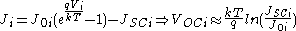
J-V characteristic
For maximum efficiency, each subcell should be operated at its optimal J-V parameters, which are not necessarily equal for each subcell. If they are different, the total current through the solar cell is the lowest of the three. By approximation, it results in the same relationship for the short-circuit current of the MJ solar cell: JSC = min (JSC1, JSC2, JSC3) where JSCi(λ) is the short-circuit current density at a given wavelength λ for the subcell i.Because of the impossibility to obtain JSC1, JSC2, JSC3 directly from the total J-V characteristic, the quantum efficiency QE(λ) is utilized. It measures the ratio between the amount of electron-hole pairs created and the incident photons at a given wavelength λ. Let φi(λ) be the photon flux of corresponding incident light in subcell iandQEi(λ) be the quantum efficiency of the subcell i. By definition, this equates to:
The value of
is obtained by linking it with the absorption coefficient, i.e. the number of photons absorbed per unit of length by a material. If it is assumed that each photon absorbed by a subcell creates an electron/hole pair (which is a good approximation), this leads to : where di is the thickness of the subcell i and is the percentage of incident light which is not absorbed by the subcell i.Similarly, because
, the following approximation can be used: .The values of
are then given by the J-V diode equation:Materials
The majority of multi-junction cells that have been produced to date use three layers, tuned to blue (on top), yellow and red (on the bottom). These cells require the use of semiconductors that can be tuned to specific frequencies, which has led to most of them being made of gallium arsenide (GaAs) compounds, often germanium for red, GaAs for yellow, and GaInP2 for blue.Gallium arsenide substrate
Dual junction cells can be made on Gallium arsenide wafers. Alloys of Indium gallium phosphideIndium gallium phosphide
Indium gallium phosphide , also called gallium indium phosphide , is a semiconductor composed of indium, gallium and phosphorus...
in the range In.5Ga.5P through In.53Ga.47P serve as the high band gap alloy. This alloy range provides for the ability to have band gaps in the range of 1.92eV to 1.87eV. The lower GaAs
Gaas
Gaas is a commune in the Landes department in Aquitaine in south-western France....
junction has a band gap of 1.42eV.
Germanium substrate
Triple junction cells consisting of Indium gallium phosphideIndium gallium phosphide
Indium gallium phosphide , also called gallium indium phosphide , is a semiconductor composed of indium, gallium and phosphorus...
, Gallium arsenide or Indium gallium arsenide
Indium gallium arsenide
Indium gallium arsenide is a semiconductor composed of indium, gallium and arsenic. It is used in high-power and high-frequency electronics because of its superior electron velocity with respect to the more common semiconductors silicon and gallium arsenide. InGaAs bandgap also makes it the...
and Germanium
Germanium
Germanium is a chemical element with the symbol Ge and atomic number 32. It is a lustrous, hard, grayish-white metalloid in the carbon group, chemically similar to its group neighbors tin and silicon. The isolated element is a semiconductor, with an appearance most similar to elemental silicon....
can be fabricated on germanium wafers. Early cells used straight gallium arsenide in the middle junction. Later cells have utilized In0.015Ga0.985As, due to the better lattice match to Ge, resulting in a lower defect density.
Due to the huge band gap difference between GaAs (1.42eV), and Ge (0.66eV), the current match is very poor, with the Ge junction operated significantly current limited.
Current efficiencies for InGaP/GaAs/Ge cells are in the mid 30% range. Lab cells using additional junctions between the GaAs and Ge junction have demonstrated efficiencies above 40%.
Indium phosphide substrate
Indium phosphide may be used as a substrate to fabricate cells with band gaps between 1.35eV and 0.74eV. Indium Phosphide has a band gap of 1.35eV. Indium gallium arsenideIndium gallium arsenide
Indium gallium arsenide is a semiconductor composed of indium, gallium and arsenic. It is used in high-power and high-frequency electronics because of its superior electron velocity with respect to the more common semiconductors silicon and gallium arsenide. InGaAs bandgap also makes it the...
(In0.53Ga0.47As) is lattice matched to Indium Phosphide with a band gap of 0.74eV. A quaternary alloy of Indium gallium arsenide phosphide can be lattice matched for any band gap in between the two.
Indium phosphide-based cells have the potential to work in tandem with gallium arsenide cells. The two cells can be optically connected in series (with the InP cell below the GaAs cell), or in parallel through the use of spectra splitting using a Dichroic filter
Dichroic filter
A dichroic filter, thin-film filter, or interference filter is a very accurate color filter used to selectively pass light of a small range of colors while reflecting other colors. By comparison, dichroic mirrors and dichroic reflectors tend to be characterized by the color of light that they...
.
Structure
All MJ photovoltaic cells use III-V semiconductor materials. GaAsSb-based heterojunction tunnel diodes, instead of conventional InGaP highly doped tunnel diodes described above, have a lower tunneling distance. Indeed, in the heterostructure formed by GaAsSb and InGaAs, the valence band of GaAsSb is higher than the valence band of the adjoining p-doped layer. Consequently, the tunneling distance dtunnel is reduced and so the tunneling current, which exponentially depends of dtunnel, is increased. Hence, the voltage is lower than that of the InGaP tunnel junction.GaAsSb heterojunction tunnel diodes offer other advantages. The same current can be achieved by using a lower doping. Secondly, because the lattice constant is larger for GaAsSb than Ge, one can use a wider range of materials for the bottom cell because more materials are lattice-matched to GaAsSb than to Ge.
Chemical components can be added to some layers. Adding about one percent of Indium
Indium
Indium is a chemical element with the symbol In and atomic number 49. This rare, very soft, malleable and easily fusible post-transition metal is chemically similar to gallium and thallium, and shows the intermediate properties between these two...
in each layer better matches lattice constants of the different layers. Without it, there is about 0.08 percent of mismatching between layers, which inhibits performance. Adding aluminium to the top cell increases its band gap to 1.96 eV, covering a larger part of the solar spectrum and obtain a higher open-circuit voltage VOC.
The theoretical efficiency of MJ solar cells is 86.8% for an infinite number of pn junctions, implying that more junctions increase efficiency. The maximum theoretical efficiency is 37, 50, 56, 72% for 1, 2, 3, 36 pn junctions, respectively, with the number of junctions increasing exponentially to achieve equal effiency increments. The exponential relationship implies that as the cell approaches the limit of efficiency, the increase cost and complexity grow rapidly. Decreasing the thickness of the top cell increases the transmission coefficient T.
Finally, an InGaP hetero-layer between the p-Ge layer and the InGaAs layer can be added in order to create automatically the n-Ge layer by scattering during MOCVD growth and increase significantly the quantum efficiency QE(λ) of the bottom cell. InGaP is advantageous because of its high scattering coefficient and low solubility in Ge.
Spectral variations
Solar spectrum at the Earth surface changes constantly depending on the weather and sun position. This results in the variation of φ(λ), QE(λ), α(λ) and thus the short-circuit currents JSCi. As a result, the current densities Ji are not necessarily matched and the total current becomes lower. These variations can be quantified using the average photon energy (APE) which is the ratio between the spectral irradiance G(λ) (the power density of the light source in a specific wavelength λ) and the total photon flux density. It can be shown that a high (low) value for APE means low (high) wavelengths spectral conditions and higher (lower) efficiencies. Thus APE is a good indicator for quantifying the effects of the solar spectrum variations on performances and has the added advantage of being independent of the device structure and the absorption profile of the device.Use of light concentrators
Light concentrators increase efficiencies and reduce the cost/efficiency ratio. The two types of light concentrators are refractive lenses like Fresnel lensFresnel lens
A Fresnel lens is a type of lens originally developed by French physicist Augustin-Jean Fresnel for lighthouses.The design allows the construction of lenses of large aperture and short focal length without the mass and volume of material that would be required by a lens of conventional design...
es and reflective dishes. Thanks to these devices, light arriving on a large surface can be concentrated on a smaller cell. The intensity concentration ratio (or “suns”) is the average intensity of the focused light divided by 0.1 W/m². If its value is X then the MJ current becomes X higher under concentrated illumination.
Using concentrations on the order of 500 to 1000, meaning that a 1 cm² cell can use the light collected from 0.1 m² (as 1 m2 equal 10000 cm2), produces the highest efficiencies seen to date. Three-layer cells are fundamentally limited to 63%, but existing commercial prototypes have already demonstrated over 40%. These cells capture about 2/3 of their theoretical maximum performance, so assuming the same is true for a non-concentrated version of the same design, one might expect a three-layer cell of 30% efficiency. This is not enough of an advantage over traditional silicon designs to make up for their extra production costs. For this reason, almost all multi-junction cell research for terrestrial use is dedicated to concentrator systems, normally using mirrors or fresnel lenses.
Using a concentrator also has the added benefit that the number of cells needed to cover a given amount of ground area is greatly reduced. A conventional system covering 1 m² would require 625 16 cm² cells, but for a concentrator system only a single cell is needed, along with a concentrator. The argument for concentrated Multi-junction cells has been that the high cost of the cells themselves would be more than offset by the reduction in total number of cells. However, the downside of the concentrator approach is that efficiency drops off very quickly under lower lighting conditions. In order to maximize its advantage over traditional cells and thus be cost competitive, the concentrator system has to track the sun as it moves to keep the light focused on the cell and maintain maximum efficiency as long as possible. This requires an expensive solar tracker
Solar tracker
A solar tracker is a generic term used to describe devices that orient various payloads toward the sun. Payloads can be photovoltaic panels, reflectors, lenses or other optical devices....
system, and offsets the potential advantages offered by multi-junction cells.
Fabrication
Multi-junction cells are expensive to produce, using techniques similar to semiconductor device fabrication, usually metalorganic vapour phase epitaxyMetalorganic vapour phase epitaxy
Metalorganic vapour phase epitaxy , also known as organometallic vapour phase epitaxy or metalorganic chemical vapour deposition , is a chemical vapour deposition method of epitaxial growth of materials, especially compound semiconductors, from the surface reaction of organic compounds or...
but on "chip" sizes on the order of centimeters. In cases where outright performance is the only consideration, these cells have become common, they are widely used in satellite
Satellite
In the context of spaceflight, a satellite is an object which has been placed into orbit by human endeavour. Such objects are sometimes called artificial satellites to distinguish them from natural satellites such as the Moon....
applications for instance, where the power-to-weight ratio
Power-to-weight ratio
Power-to-weight ratio is a calculation commonly applied to engines and mobile power sources to enable the comparison of one unit or design to another. Power-to-weight ratio is a measurement of actual performance of any engine or power sources...
overwhelms practically every other cost.
Comparison with other technologies
There are four main categories of photovoltaic cells: c-Si solar cells, thin film solar cellThin film solar cell
A thin-film solar cell , also called a thin-film photovoltaic cell , is a solar cell that is made by depositing one or more thin layers of photovoltaic material on a substrate...
s, MJ solar cells and new technologies (including organic solar cells).
| Technology | η (%) | VOC (V) | ISC (A) | W/m² | t (µm) |
|---|---|---|---|---|---|
| u c-Si | 24.7 | 0.5 | 0.8 | 63 | 100 |
| p c-Si | 20.3 | 0.615 | 8.35 | 211 | 200 |
| a-Si | 11.1 | 6.3 | 0.0089 | 33 | 1 |
| CdTe | 16.5 | 0.86 | 0.029 | – | 5 |
| CIGS | 19.5 | – | – | – | 1 |
| MJ | 40.7 | 2.6 | 1.81 | 476 | 140 |
MJ solar cells and other photovoltaic devices have significant differences (see the table above). Physically, the main property of a MJ solar cell is having more than one pn junction in order to catch a larger photon energy spectrum while the main property of the thin film solar cell
Thin film solar cell
A thin-film solar cell , also called a thin-film photovoltaic cell , is a solar cell that is made by depositing one or more thin layers of photovoltaic material on a substrate...
is to use thin films instead of thick layers in order to decrease the cost efficiency ratio. As of 2010, MJ solar panels are more expensive than others. These differences imply different applications: MJ solar cells are preferred in space and c-Si solar cells for terrestrian applications.
The efficiencies of solar cells and Si solar technology are relatively stable, while the efficiency of solar modules and multi-junction technology are progressing.
Measurements on MJ solar cells are usually made in laboratory, using light concentrators (this is often not the case for the other cells) and under standard test conditions (STCs). STCs prescribe, for terrestrial applications, the AM1.5 spectrum as the reference. This air mass (AM) corresponds to a fixed position of the sun in the sky of 48° and a fixed power of 833 W/m². Therefore, spectral variations of incident light and environmental parameters are not taken into account under STC.
Consequently, performance of MJ solar cells in terrestrial environment is inferior to that achieved in laboratory. Moreover, MJ solar cells are designed such that currents are matched under STC, but not necessarily under field conditions. One can use QE(λ) to compare performances of different technologies, but QE(λ) contains no information on the matching of currents of subcells. An important comparison point is rather the output power per unit area generated with the same incident light.
Applications
As of 2010, the cost of MJ solar cells was too high to allow use outside of specialized applications. The high cost is mainly due to the complex structure and the high price of materials. Nevertheless, with light concentrators under illumination of at least 400 suns, MJ solar panelsConcentrated photovoltaics
Concentrated photovoltaic technology uses optics such as lenses to concentrate a large amount of sunlight onto a small area of solar photovoltaic materials to generate electricity...
become practical.
MJ cells are currently being utilized in the Mars rover missions.
The environment in space is quite different. Because there is no atmosphere, the solar spectrum is different (AM0). The cells have a poor current match due to a greater photon flux of photons above 1.87eV vs. those between 1.87eV and 1.42eV. This results in too little current in the GaAs junction, and hampers the overall efficiency since the InGaP junction operates below MPP current and the GaAs junction operates above MPP current. To improve current match, the InGaP layer is intentionally thinned to allow additional photons to penetrate to the lower GaAs layer.
In terrestrial concentrating applications, the scatter of blue light by the atmosphere reduces the photon flux above 1.87eV, better balancing the junction currents.Radiation particles that are no longer filtered can cause damage the cell. There are two kinds of damage: ionisation and atomic displacement. Still, MJ cells offer higher radiation resistance, higher efficiency and a lower temperature coefficient.
See also
- List of semiconductor materials
- Organic photovoltaic cell
- p-i-n and n-i-p