
Multigate device
Encyclopedia
A multigate device or multiple gate field-effect transistor(MuGFET) refers to a MOSFET
which incorporates more than one gate into a single device. The multiple gates may be controlled by a single gate electrode, wherein the multiple gate surfaces act electrically as a single gate, or by independent gate electrodes. A multigate device employing independent gate electrodes is sometimes called a Multiple Independent Gate Field Effect Transistor or MIGFET. Multigate transistor
s are one of several strategies being developed by CMOS
semiconductor
manufacturers to create ever-smaller microprocessors and memory cells
, colloquially referred to as extending Moore's Law
.
Development efforts into multigate transistors have been reported by AMD
, Hitachi
, IBM
, Infineon Technologies
, Intel Corporation
, TSMC
, Freescale Semiconductor
, University of California, Berkeley
and others and the ITRS
predicts that such devices will be the cornerstone of sub-32 nm technologies.
The primary roadblock to widespread implementation is manufacturability, as both planar and non-planar designs present significant challenges, especially with respect to lithography
and patterning. Other complementary strategies for device scaling include channel strain engineering
, silicon-on-insulator
-based technologies, and high-k/metal gate materials.
In a multigate device, the channel is surrounded by several gates on multiple surfaces, allowing more effective suppression of "off-state" leakage current. Multiple gates also allow enhanced current in the "on" state, also known as drive current. These advantages translate to lower power consumption and enhanced device performance. Nonplanar devices are also more compact than conventional planar transistors, enabling higher transistor density which translates to smaller overall microelectronics.
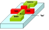
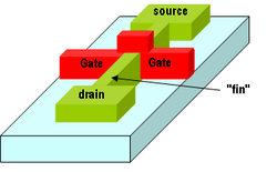 The term FinFET was coined by University of California, Berkeley researchers (Profs. Chenming Hu, Tsu-Jae King-Liu and Jeffrey Bokor) to describe a nonplanar, double-gate transistor built on an SOI
substrate, based on the earlier DELTA (single-gate) transistor design. The distinguishing characteristic of the FinFET is that the conducting channel is wrapped by a thin silicon "fin", which forms the gate of the device. The thickness of the fin (measured in the direction from source to drain) determines the effective channel length of the device.
In current usage the term FinFET has a less precise definition. Among microprocessor
manufacturers, AMD, IBM
, and Motorola
describe their double-gate development efforts as FinFET development whereas Intel avoids using the term to describe their closely related tri-gate http://www.intel.com/technology/silicon/integrated_cmos.htm architecture. In the technical literature, FinFET is used somewhat generically to describe any fin-based, multigate transistor architecture regardless of number of gates.
A 25-nm transistor operating on just 0.7 Volt
was demonstrated in December 2002 by Taiwan Semiconductor Manufacturing Company. The "Omega FinFET" design, named after the similarity between the Greek letter "Omega
" and the shape in which the gate wraps around the source/drain structure, has a gate delay of just 0.39 picosecond
(ps) for the N-type transistor and 0.88 ps for the P-type.
 Tri-gate or 3-D are terms used by Intel Corporation to describe the nonplanar transistor architecture planned for use in future microprocessor
s. These transistors employ a single gate stacked on top of two vertical gates allowing for essentially three times the surface area for electron
s to travel. Intel reports that their tri-gate transistors reduce leakage
and consume far less power
than current transistors. This allows up to 37% higher speed, and a power consumption at under 50% of the previous type of transistors used by Intel.
Intel explains, "The additional control enables as much transistor current flowing as possible when the transistor is in the 'on' state (for performance), and as close to zero as possible when it is in the 'off' state (to minimize power), and enables the transistor to switch very quickly between the two states (again, for performance)." Intel has stated that all products after Sandy Bridge will be based upon this 3D design.
Intel was the first company to announce this technology. In September 2002 , Intel announced their creation of 'Triple-Gate Transistors' to maximize 'transistor switching performance and decreases power-wasting leakage'. No further announcements of this technology were made until Intel's announcement in May 2011 although it was stated at IDF 2011, that they demonstrated a working SRAM chip based on this technology at IDF 2009.
, Intel plans to release a new line of CPUs, termed Ivy Bridge, which feature tri-gate transistors. Intel has been working on its tri-gate architecture since 2002, but it took until 2011 to work out mass production issues. The new style of transistor was described on May 4, 2011, in San Francisco. Intel factories are expected to make upgrades over 2011 and 2012 to be able to manufacture the Ivy Bridge CPUs. As well as being used in Intel's Ivy Bridge chips for desktop PCs, the new transistors will also be used in Intel's Atom chips for low powered devices.
The term tri-gate is sometimes used generically to denote any multigate FET with three effective gates or channels.
.
MOSFET
The metal–oxide–semiconductor field-effect transistor is a transistor used for amplifying or switching electronic signals. The basic principle of this kind of transistor was first patented by Julius Edgar Lilienfeld in 1925...
which incorporates more than one gate into a single device. The multiple gates may be controlled by a single gate electrode, wherein the multiple gate surfaces act electrically as a single gate, or by independent gate electrodes. A multigate device employing independent gate electrodes is sometimes called a Multiple Independent Gate Field Effect Transistor or MIGFET. Multigate transistor
Transistor
A transistor is a semiconductor device used to amplify and switch electronic signals and power. It is composed of a semiconductor material with at least three terminals for connection to an external circuit. A voltage or current applied to one pair of the transistor's terminals changes the current...
s are one of several strategies being developed by CMOS
CMOS
Complementary metal–oxide–semiconductor is a technology for constructing integrated circuits. CMOS technology is used in microprocessors, microcontrollers, static RAM, and other digital logic circuits...
semiconductor
Semiconductor
A semiconductor is a material with electrical conductivity due to electron flow intermediate in magnitude between that of a conductor and an insulator. This means a conductivity roughly in the range of 103 to 10−8 siemens per centimeter...
manufacturers to create ever-smaller microprocessors and memory cells
Computer storage
Computer data storage, often called storage or memory, refers to computer components and recording media that retain digital data. Data storage is one of the core functions and fundamental components of computers....
, colloquially referred to as extending Moore's Law
Moore's Law
Moore's law describes a long-term trend in the history of computing hardware: the number of transistors that can be placed inexpensively on an integrated circuit doubles approximately every two years....
.
Development efforts into multigate transistors have been reported by AMD
Advanced Micro Devices
Advanced Micro Devices, Inc. or AMD is an American multinational semiconductor company based in Sunnyvale, California, that develops computer processors and related technologies for commercial and consumer markets...
, Hitachi
Hitachi, Ltd.
is a Japanese multinational conglomerate headquartered in Marunouchi 1-chome, Chiyoda, Tokyo, Japan. The company is the parent of the Hitachi Group as part of the larger DKB Group companies...
, IBM
IBM
International Business Machines Corporation or IBM is an American multinational technology and consulting corporation headquartered in Armonk, New York, United States. IBM manufactures and sells computer hardware and software, and it offers infrastructure, hosting and consulting services in areas...
, Infineon Technologies
Infineon Technologies
Infineon Technologies AG is a German semiconductor manufacturer and was founded on April 1, 1999, when the semiconductor operations of the parent company Siemens AG were spun off to form a separate legal entity. , Infineon has 25,149 employees worldwide...
, Intel Corporation
Intel Corporation
Intel Corporation is an American multinational semiconductor chip maker corporation headquartered in Santa Clara, California, United States and the world's largest semiconductor chip maker, based on revenue. It is the inventor of the x86 series of microprocessors, the processors found in most...
, TSMC
TSMC
Taiwan Semiconductor Manufacturing Company, Limited or TSMC is the world's largest dedicated independent semiconductor foundry, with its headquarters and main operations located in the Hsinchu Science Park in Hsinchu, Taiwan.-Overview:...
, Freescale Semiconductor
Freescale Semiconductor
Freescale Semiconductor, Inc. is a producer and designer of embedded hardware, with 17 billion semiconductor chips in use around the world. The company focuses on the automotive, consumer, industrial and networking markets with its product portfolio including microprocessors, microcontrollers,...
, University of California, Berkeley
University of California, Berkeley
The University of California, Berkeley , is a teaching and research university established in 1868 and located in Berkeley, California, USA...
and others and the ITRS
International Technology Roadmap for Semiconductors
The International Technology Roadmap for Semiconductors is a set of documents produced by a group of semiconductor industry experts. These experts are representative of the sponsoring organisations which include the Semiconductor Industry Associations of the US, Europe, Japan, South Korea and...
predicts that such devices will be the cornerstone of sub-32 nm technologies.
The primary roadblock to widespread implementation is manufacturability, as both planar and non-planar designs present significant challenges, especially with respect to lithography
Photolithography
Photolithography is a process used in microfabrication to selectively remove parts of a thin film or the bulk of a substrate. It uses light to transfer a geometric pattern from a photomask to a light-sensitive chemical "photoresist", or simply "resist," on the substrate...
and patterning. Other complementary strategies for device scaling include channel strain engineering
Strain engineering
Strain engineering refers to a general strategy employed in semiconductor manufacturing to enhance device performance. Performance benefits are achieved by modulating strain in the transistor channel, which enhances electron mobility and thereby conductivity through the channel.-Strain...
, silicon-on-insulator
Silicon on insulator
Silicon on insulator technology refers to the use of a layered silicon-insulator-silicon substrate in place of conventional silicon substrates in semiconductor manufacturing, especially microelectronics, to reduce parasitic device capacitance and thereby improving performance...
-based technologies, and high-k/metal gate materials.
Industry need
Planar transistors have been the core of integrated circuits for several decades, during which the size of the individual transistors has steadily decreased. As the size decreases, planar transistors increasingly suffer from the undesirable short-channel effect, especially "off-state" leakage current, which increases the idle power required by the device.In a multigate device, the channel is surrounded by several gates on multiple surfaces, allowing more effective suppression of "off-state" leakage current. Multiple gates also allow enhanced current in the "on" state, also known as drive current. These advantages translate to lower power consumption and enhanced device performance. Nonplanar devices are also more compact than conventional planar transistors, enabling higher transistor density which translates to smaller overall microelectronics.
Integration challenges
The primary challenges to integrating nonplanar multigate devices into conventional semiconductor manufacturing processes include:- Fabrication of a thin silicon "fin" tens of nanometers wide
- Fabrication of matched gates on multiple sides of the fin
Varieties
Dozens of multigate transistor variants may be found in the literature. In general, these variants may be differentiated and classified in terms of architecture (planar vs. non-planar design) and number of channels/gates (2, 3, or 4).Planar double-gate transistors
Planar double-gate transistors employ conventional planar (layer by layer) manufacturing processes to create double-gate devices, avoiding more stringent lithography requirements associated with non-planar, vertical transistor structures. In planar double-gate transistors the channel is sandwiched between two independently fabricated gate/gate oxide stacks. The primary challenge in fabricating such structures is achieving satisfactory self-alignment between the upper and lower gates.Flexfet
Flexfet is a planar, independently-double-gated transistor with a damascene metal top gate MOSFET and an implanted JFET bottom gate that are self-aligned in a gate trench. This device is highly scalable due to its sub-lithographic channel length; non-implanted ultra-shallow source and drain extensions; non-epi raised source and drain regions; and gate-last flow. Flexfet is a true double-gate transistor in that (1) both the top and bottom gates provide transistor operation, and (2) the operation of the gates is coupled such that the top gate operation affects the bottom gate operation and vice versa. Flexfet was developed, and is manufactured, by American Semiconductor, Inc.FinFETs
Silicon on insulator
Silicon on insulator technology refers to the use of a layered silicon-insulator-silicon substrate in place of conventional silicon substrates in semiconductor manufacturing, especially microelectronics, to reduce parasitic device capacitance and thereby improving performance...
substrate, based on the earlier DELTA (single-gate) transistor design. The distinguishing characteristic of the FinFET is that the conducting channel is wrapped by a thin silicon "fin", which forms the gate of the device. The thickness of the fin (measured in the direction from source to drain) determines the effective channel length of the device.
In current usage the term FinFET has a less precise definition. Among microprocessor
Microprocessor
A microprocessor incorporates the functions of a computer's central processing unit on a single integrated circuit, or at most a few integrated circuits. It is a multipurpose, programmable device that accepts digital data as input, processes it according to instructions stored in its memory, and...
manufacturers, AMD, IBM
IBM
International Business Machines Corporation or IBM is an American multinational technology and consulting corporation headquartered in Armonk, New York, United States. IBM manufactures and sells computer hardware and software, and it offers infrastructure, hosting and consulting services in areas...
, and Motorola
Motorola
Motorola, Inc. was an American multinational telecommunications company based in Schaumburg, Illinois, which was eventually divided into two independent public companies, Motorola Mobility and Motorola Solutions on January 4, 2011, after losing $4.3 billion from 2007 to 2009...
describe their double-gate development efforts as FinFET development whereas Intel avoids using the term to describe their closely related tri-gate http://www.intel.com/technology/silicon/integrated_cmos.htm architecture. In the technical literature, FinFET is used somewhat generically to describe any fin-based, multigate transistor architecture regardless of number of gates.
A 25-nm transistor operating on just 0.7 Volt
Volt
The volt is the SI derived unit for electric potential, electric potential difference, and electromotive force. The volt is named in honor of the Italian physicist Alessandro Volta , who invented the voltaic pile, possibly the first chemical battery.- Definition :A single volt is defined as the...
was demonstrated in December 2002 by Taiwan Semiconductor Manufacturing Company. The "Omega FinFET" design, named after the similarity between the Greek letter "Omega
Omega
Omega is the 24th and last letter of the Greek alphabet. In the Greek numeric system, it has a value of 800. The word literally means "great O" , as opposed to omicron, which means "little O"...
" and the shape in which the gate wraps around the source/drain structure, has a gate delay of just 0.39 picosecond
Picosecond
A picosecond is 10−12 of a second. That is one trillionth, or one millionth of one millionth of a second, or 0.000 000 000 001 seconds. A picosecond is to one second as one second is to 31,700 years....
(ps) for the N-type transistor and 0.88 ps for the P-type.
Tri-gate transistors
Microprocessor
A microprocessor incorporates the functions of a computer's central processing unit on a single integrated circuit, or at most a few integrated circuits. It is a multipurpose, programmable device that accepts digital data as input, processes it according to instructions stored in its memory, and...
s. These transistors employ a single gate stacked on top of two vertical gates allowing for essentially three times the surface area for electron
Electron
The electron is a subatomic particle with a negative elementary electric charge. It has no known components or substructure; in other words, it is generally thought to be an elementary particle. An electron has a mass that is approximately 1/1836 that of the proton...
s to travel. Intel reports that their tri-gate transistors reduce leakage
Subthreshold leakage
The Subthreshold conduction or the subthreshold leakage or the subthreshold drain current is the current that flows between the source and drain of a MOSFET when the transistor is in subthreshold region, or weak-inversion region, that is, for gate-to-source voltages below the threshold voltage. The...
and consume far less power
Electric power
Electric power is the rate at which electric energy is transferred by an electric circuit. The SI unit of power is the watt.-Circuits:Electric power, like mechanical power, is represented by the letter P in electrical equations...
than current transistors. This allows up to 37% higher speed, and a power consumption at under 50% of the previous type of transistors used by Intel.
Intel explains, "The additional control enables as much transistor current flowing as possible when the transistor is in the 'on' state (for performance), and as close to zero as possible when it is in the 'off' state (to minimize power), and enables the transistor to switch very quickly between the two states (again, for performance)." Intel has stated that all products after Sandy Bridge will be based upon this 3D design.
Intel was the first company to announce this technology. In September 2002 , Intel announced their creation of 'Triple-Gate Transistors' to maximize 'transistor switching performance and decreases power-wasting leakage'. No further announcements of this technology were made until Intel's announcement in May 2011 although it was stated at IDF 2011, that they demonstrated a working SRAM chip based on this technology at IDF 2009.
, Intel plans to release a new line of CPUs, termed Ivy Bridge, which feature tri-gate transistors. Intel has been working on its tri-gate architecture since 2002, but it took until 2011 to work out mass production issues. The new style of transistor was described on May 4, 2011, in San Francisco. Intel factories are expected to make upgrades over 2011 and 2012 to be able to manufacture the Ivy Bridge CPUs. As well as being used in Intel's Ivy Bridge chips for desktop PCs, the new transistors will also be used in Intel's Atom chips for low powered devices.
The term tri-gate is sometimes used generically to denote any multigate FET with three effective gates or channels.
Gate-all-around (GAA) FETs
Gate-all-around FETs are similar in concept to FinFETs except that the gate material surrounds the channel region on all sides. Depending on design, gate-all-around FETs can have two or four effective gates. Gate-all-around FETs have been successfully built around silicon nanowireNanowire
A nanowire is a nanostructure, with the diameter of the order of a nanometer . Alternatively, nanowires can be defined as structures that have a thickness or diameter constrained to tens of nanometers or less and an unconstrained length. At these scales, quantum mechanical effects are important —...
.