
List of Intel microprocessors
Encyclopedia
This generational and chronological list of Intel microprocessors attempts to present all of Intel
's processor
s from the pioneering 4-bit 4004
(1971) to the present high-end offerings, which include the 64-bit Itanium 2 (2002), Intel Core 2
, and Xeon
5100 and 7100 series processors (2006). Concise technical data is given for each product.
Intel 4004
MCS-4 Family:
MCS-85 Family:
MCS-48 family:
MCS-51 Family:
MCS-96
 Introduced 3rd Qtr, 1974
Members of the family
Bus Width 2-n bits data/address (depending on number of slices used)
8086
8088
80186
80286
iAPX 432
i960 aka 80960
80386SX (chronological entry)
80376 (chronological entry)
i860 aka 80860
XScale
80386DX
80960 (i960) (chronological entry)
80376
80860 (i860) (chronological entry)
80486DX (chronological entry)
80486SX/DX2/SL, Pentium, 80486DX4 (chronological entries)
80386EX
80386SL (chronological entry)
80486SX
80486DX2
Runs at twice the speed of the external bus (FSB).
80486SL
Pentium (chronological entry)
80486DX4
32-bit processors: P6
Pentium Pro
Pentium II
Celeron
Pentium II Xeon (chronological entry)
Pentium III
Pentium II and III Xeon
Celeron
XScale (chronological entry)
Pentium 4 (not 4EE, 4E, 4F), Itanium, P4-based Xeon, Itanium 2 (chronological entries)
Celeron
Pentium M
Celeron M
Intel Core
Dual-Core Xeon
Pentium 4
Itanium (chronological entry)
Xeon
Itanium 2 (chronological entry)
Pentium D
Xeon
Xeon
Intel Core 2
Pentium Dual Core
32-bit processors: Intel 32 – Intel Atom
TODO: http://ark.intel.com/ProductCollection.aspx?familyId=29035
TODO:
Westmere
Xeon
brand in 1993. However, numerical codes, in the 805xx range, continued to be assigned to these processors for internal and part numbering uses. The following is a list of such product codes in numerical order:
Intel Corporation
Intel Corporation is an American multinational semiconductor chip maker corporation headquartered in Santa Clara, California, United States and the world's largest semiconductor chip maker, based on revenue. It is the inventor of the x86 series of microprocessors, the processors found in most...
's processor
Microprocessor
A microprocessor incorporates the functions of a computer's central processing unit on a single integrated circuit, or at most a few integrated circuits. It is a multipurpose, programmable device that accepts digital data as input, processes it according to instructions stored in its memory, and...
s from the pioneering 4-bit 4004
Intel 4004
The Intel 4004 was a 4-bit central processing unit released by Intel Corporation in 1971. It was the first complete CPU on one chip, and also the first commercially available microprocessor...
(1971) to the present high-end offerings, which include the 64-bit Itanium 2 (2002), Intel Core 2
Intel Core 2
Core 2 is a brand encompassing a range of Intel's consumer 64-bit x86-64 single-, dual-, and quad-core microprocessors based on the Core microarchitecture. The single- and dual-core models are single-die, whereas the quad-core models comprise two dies, each containing two cores, packaged in a...
, and Xeon
Xeon
The Xeon is a brand of multiprocessing- or multi-socket-capable x86 microprocessors from Intel Corporation targeted at the non-consumer server, workstation and embedded system markets.-Overview:...
5100 and 7100 series processors (2006). Concise technical data is given for each product.
Intel 4004Intel 4004The Intel 4004 was a 4-bit central processing unit released by Intel Corporation in 1971. It was the first complete CPU on one chip, and also the first commercially available microprocessor...
: first single-chip microprocessor
- Introduced November 15, 1971
- Clock rate 740 kHz
- 0.07 MIPS
- Bus Width 8 bitBitA bit is the basic unit of information in computing and telecommunications; it is the amount of information stored by a digital device or other physical system that exists in one of two possible distinct states...
s (multiplexed address/data due to limited pins) - PMOSPMOS logicP-type metal-oxide-semiconductor logic uses p-type metal-oxide-semiconductor field effect transistors to implement logic gates and other digital circuits...
- Number of Transistors 2,300 at 10 µmMicrometreA micrometer , is by definition 1×10⁻⁶ of a meter .In plain English, it means one-millionth of a meter . Its unit symbol in the International System of Units is μm...
- Addressable Memory 640 byteByteThe byte is a unit of digital information in computing and telecommunications that most commonly consists of eight bits. Historically, a byte was the number of bits used to encode a single character of text in a computer and for this reason it is the basic addressable element in many computer...
s - Program Memory 4 KB (4 KBKilobyteThe kilobyte is a multiple of the unit byte for digital information. Although the prefix kilo- means 1000, the term kilobyte and symbol KB have historically been used to refer to either 1024 bytes or 1000 bytes, dependent upon context, in the fields of computer science and information...
) - One of the earliest Commercial Microprocessors (cf. Four Phase Systems AL1Four Phase Systems AL1Four-Phase Systems was a computer company, founded by Lee Boysel and others, which built one of the earliest computers using semiconductor main memory and LSI MOS logic. The company was incorporated in February 1969 and had moderate commercial success...
, F14 CADC) - Originally designed to be used in BusicomBusicomBusicom was a Japanese company that owned the rights to the first microprocessor, the Intel 4004, which they created in partnership with Intel in 1970....
calculator
MCS-4 Family:
- 4004-CPU
- 4001-ROMRead-only memoryRead-only memory is a class of storage medium used in computers and other electronic devices. Data stored in ROM cannot be modified, or can be modified only slowly or with difficulty, so it is mainly used to distribute firmware .In its strictest sense, ROM refers only...
& 4 Bit Port - 4002-RAMRam-Animals:*Ram, an uncastrated male sheep*Ram cichlid, a species of freshwater fish endemic to Colombia and Venezuela-Military:*Battering ram*Ramming, a military tactic in which one vehicle runs into another...
& 4 Bit Port - 4003-10 Bit Shift Register
- 4008-Memory+I/O Interface
- 4009-Memory+I/O Interface
Intel 4040
MCS-40 Family:- 4040-CPU
- 4101-1024-bit (256 × 4) Static RAM with separate I/O
- 4201-4 MHz Clock Generator
- 4207-General Purpose Byte I/O Port
- 4209-General Purpose Byte I/O Port
- 4211-General Purpose Byte I/O Port
- 4265-Programmable General Purpose I/O Device
- 4269-Programmable Keyboard Display Device
- 4289-Standard Memory Interface for MCS-4/40
- 4308-8192-bit (1024 × 8) ROM w/ 4-bit I/O Ports
- 4316-16384-bit (2048 × 8) Static ROM
- 4702-2048-bit (256 × 8) EPROM
- 4801–5.185 MHz Clock Generator Crystal for 4004/4201A or 4040/4201A
8008
- Introduced April 1, 1972
- Clock rate 500 kHz (8008–1: 800 kHz)
- 0.05 MIPS
- Bus Width 8 bits (multiplexed address/data due to limited pins)
- Enhancement load PMOSPMOS logicP-type metal-oxide-semiconductor logic uses p-type metal-oxide-semiconductor field effect transistors to implement logic gates and other digital circuits...
logic - Number of Transistors 3,500 at 10 µm
- Addressable memory 16 KB
- Typical in early 8 bit microcomputers, dumb terminals, general calculators, bottling machines
- Developed in tandem with 4004
- Originally intended for use in the Datapoint 2200Datapoint 2200The Datapoint 2200 was a mass-produced programmable terminal, designed by Phil Ray and Gus Roche, announced by Computer Terminal Corporation in June, 1970...
microcomputer - Key volume deployment in Texas Instruments 742 microcomputer in >3,000 Ford dealerships
8080
- Introduced April 1, 1974
- Clock rate 2 MHz (very rare 8080B: 3 MHz)
- 0.64 MIPS
- Bus Width 8 bits data, 16 bits address
- Enhancement load NMOSNMOS logicN-type metal-oxide-semiconductor logic uses n-type metal-oxide-semiconductor field effect transistors to implement logic gates and other digital circuits...
logic - Number of Transistors 6,000
- Assembly languageAssembly languageAn assembly language is a low-level programming language for computers, microprocessors, microcontrollers, and other programmable devices. It implements a symbolic representation of the machine codes and other constants needed to program a given CPU architecture...
downwards compatible with 8008. - Addressable memory 64 KB
- Up to 10X the performance of the 8008
- Used in the Altair 8800Altair 8800The MITS Altair 8800 was a microcomputer design from 1975 based on the Intel 8080 CPU and sold by mail order through advertisements in Popular Electronics, Radio-Electronics and other hobbyist magazines. The designers hoped to sell only a few hundred build-it-yourself kits to hobbyists, and were...
, Traffic light controllerTraffic lightTraffic lights, which may also be known as stoplights, traffic lamps, traffic signals, signal lights, robots or semaphore, are signalling devices positioned at road intersections, pedestrian crossings and other locations to control competing flows of traffic...
, cruise missileCruise missileA cruise missile is a guided missile that carries an explosive payload and is propelled, usually by a jet engine, towards a land-based or sea-based target. Cruise missiles are designed to deliver a large warhead over long distances with high accuracy... - Required six support chips versus 20 for the 8008
8085
- Introduced March 1976
- Clock rate 3 MHz
- 0.37 MIPS
- Bus Width 8 bits data, 16 bits address
- Depletion load NMOSNMOS logicN-type metal-oxide-semiconductor logic uses n-type metal-oxide-semiconductor field effect transistors to implement logic gates and other digital circuits...
logic - Number of Transistors 6,500 at 3 µm3 µm processThe 3 µm process process refers to the level of semiconductor process technology that was reached around 1975 timeframe by the leading semiconductor companies, like Intel.-Products featuring 3 µm manufacturing process:...
- Binary compatible downwards with the 8080.
- Used in Toledo scalesMettler ToledoMettler-Toledo is a manufacturer of scales and analytical instruments. It was formed by the merging of two companies: Mettler, based in Switzerland, and Toledo Scale, based in Columbus, Ohio, USA...
. Also was used as a computer peripheral controller – modems, harddisks,printers, etc... - CMOSCMOSComplementary metal–oxide–semiconductor is a technology for constructing integrated circuits. CMOS technology is used in microprocessors, microcontrollers, static RAM, and other digital logic circuits...
80C85 in Mars Sojourner, Radio Shack Model 100 portableTRS-80 Model 100 lineThe TRS-80 Model 100 was an early portable computer introduced in 1983. It was one of the first notebook-style computers, featuring a keyboard and liquid crystal display, battery powered, in a package roughly the size and shape of notepad or large book....
. - High level of integration, operating for the first time on a single 5 volt power supply, from 12 volts previously. Also featured serial I/O,3 maskable interrupts,1 Non-maskable interrupt,1 externally expandable interrupt w/[8259],status,DMA.
MCS-85 Family:
- 8155-RAM+ 3 I/O Ports+Timer "Active Low CS"
- 8185-SRAM
- 8202-Dynamic RAM Controller
- 8203-Dynamic RAM Controller
- 8205-1 Of 8 Binary Decoder
- 8206-Error Detection & Correction Unit
- 8207-DRAM Controller
- 8210-TTL To MOS Shifter & High Voltage Clock Driver
- 8216-4 Bit Parallel Bidirectional Bus Driver
- 8219-Bus Controller
- 8222-Dynamic RAM Refresh Controller
- 8226-4 Bit Parallel Bidirectional Bus Driver
- 8232-Floating Point Processor
- 8237-DMA ControllerIntel 8237Intel 8237 is a direct memory access controller , a part of the MCS 85 microprocessor family. It was used as the DMA controller in the original IBM PC and IBM XT...
- 8251-Communication Controller
- 8253-Programmable Interval TimerIntel 8253The Intel 8253 and 8254 are Programmable Interval Timers , which perform timing and counting functions. They were primarily designed for the Intel 8080/8085-processors, but later used in x86-systems...
- 8254-Programmable Interval Timer
- 8255-Programmable Peripheral InterfaceIntel 8255The Intel 8255 Programmable Peripheral Interface chip is a peripheral chip originally developed for the Intel 8085 microprocessor, and as such is a member of a large array of such chips, known as the MCS-85 Family. This chip was later also used with the Intel 8086 and its descendants.It was later...
- 8256-Multifunction Support Controller
- 8257-DMA Controller
- 8259-Programmable Interrupt ControllerIntel 8259The Intel 8259 is a Programmable Interrupt Controller designed for the Intel 8085 and Intel 8086 microprocessors. The initial part was 8259, a later A suffix version was upward compatible and usable with the 8086 or 8088 processor...
- 8271-Programmable Floppy Disk Controller
- 8272-Single/Double Density Floppy Disk Controller
- 8273-Programmable HDLC/SDLC Protocol Controller
- 8274-Multi-Protocol Serial Controller
- 8275-CRT Controller
- 8276-Small System CRT Controller
- 8279-KeyBoard/Display Controller
- 8283-8-bit Inverting Latch with Output Buffer
- 8291-GPIB Talker/Listener
- 8292-GPIB Controller
- 8293-GPIB Transceiver
- 8294-Data Encryption/Decryption Unit+1 O/P Port
- 8295-Dot Matrix Printer Controller
- 8296-GPIB Transceiver
- 8297-GPIB Transceiver
- 8355-16,384-bit (2048 × 8) ROM with I/O
- 8755-EPROM+2 I/O Ports
Intel 8048
- Single accumulatorAccumulator (computing)In a computer's central processing unit , an accumulator is a register in which intermediate arithmetic and logic results are stored. Without a register like an accumulator, it would be necessary to write the result of each calculation to main memory, perhaps only to be read right back again for...
Harvard architectureHarvard architectureThe Harvard architecture is a computer architecture with physically separate storage and signal pathways for instructions and data. The term originated from the Harvard Mark I relay-based computer, which stored instructions on punched tape and data in electro-mechanical counters...
MCS-48 family:
- 8020-Single-Component 8-Bit Microcontroller
- 8021-Single-Component 8-Bit Microcontroller
- 8022-Single-Component 8-Bit Microcontroller With On Chip A/D Converter
- 8035-Single-Component 8-Bit Microcontroller
- 8039-Single-Component 8-Bit Microcontroller
- 8040-Single-Component 8-Bit Microcontroller
- 8041-Universal Peripheral Interface 8-Bit Slave Microcontroller
- 8641-Universal Peripheral Interface 8-Bit Slave Microcontroller
- 8741-Universal Peripheral Interface 8-Bit Slave Microcontroller
- 8042-Universal Peripheral Interface 8-Bit Slave Microcontroller
- 8742-Universal Peripheral Interface 8-Bit Slave Microcontroller
- 8243-Input/Output Expander
- 8048-Single-Component 8-Bit Microcontroller
- 8048-Single-Component 8-Bit Microcontroller
- 8748-Single-Component 8-Bit Microcontroller
- 8048-Single-Component 8-Bit Microcontroller
- 8049-Single-Component 8-Bit Microcontroller
- 8749-Single-Component 8-Bit Microcontroller
- 8050-Single-Component 8-Bit Microcontroller
Intel 8051
- Single accumulatorAccumulator (computing)In a computer's central processing unit , an accumulator is a register in which intermediate arithmetic and logic results are stored. Without a register like an accumulator, it would be necessary to write the result of each calculation to main memory, perhaps only to be read right back again for...
Harvard architectureHarvard architectureThe Harvard architecture is a computer architecture with physically separate storage and signal pathways for instructions and data. The term originated from the Harvard Mark I relay-based computer, which stored instructions on punched tape and data in electro-mechanical counters...
MCS-51 Family:
- 8031-8-Bit Control-Oriented Microcontroller
- 8032-8-Bit Control-Oriented Microcontroller
- 8044-High Performance 8-Bit Microcontroller
- 8344-High Performance 8-Bit Microcontroller
- 8744-High Performance 8-Bit Microcontroller
- 8051-8-Bit Control-Oriented Microcontroller
- 8052-8-Bit Control-Oriented Microcontroller
- 8054-8-Bit Control-Oriented Microcontroller
- 8058-8-Bit Control-Oriented Microcontroller
- 8351-8-Bit Control-Oriented Microcontroller
- 8352-8-Bit Control-Oriented Microcontroller
- 8354-8-Bit Control-Oriented Microcontroller
- 8358-8-Bit Control-Oriented Microcontroller
- 8751-8-Bit Control-Oriented Microcontroller
- 8752-8-Bit Control-Oriented Microcontroller
- 8754-8-Bit Control-Oriented Microcontroller
- 8758-8-Bit Control-Oriented Microcontroller
- 80151-8-Bit Control-Oriented Microcontroller
- 83151-8-Bit Control-Oriented Microcontroller
- 87151-8-Bit Control-Oriented Microcontroller
- 80152-8-Bit Control-Oriented Microcontroller
- 83152-8-Bit Control-Oriented Microcontroller
- 80251-8-Bit Control-Oriented Microcontroller
- 87251-8-Bit Control-Oriented Microcontroller
MCS-96Intel MCS-96The Intel MCS-96 is a family of microcontrollers commonly used in embedded systems. The family is often referred to as the 8xC196 family, or 80196, the most popular MCU in the family. These MCUs are commonly used in hard disk drives, modems, printers, pattern recognition and motor control. In...
Family
- 8094-16-Bit Microcontroller (48-Pin ROMLess Without A/D)
- 8095-16-Bit Microcontroller (48-Pin ROMLess With A/D)
- 8096-16-Bit Microcontroller (68-Pin ROMLess Without A/D)
- 8097-16-Bit Microcontroller (68-Pin ROMLess With A/D)
- 8394-16-Bit Microcontroller (48-Pin With ROM Without A/D)
- 8395-16-Bit Microcontroller (48-Pin With ROM With A/D)
- 8396-16-Bit Microcontroller (68-Pin With ROM Without A/D)]
- 8397-16-Bit Microcontroller (68-Pin With ROM With A/D)
- 8794-16-Bit Microcontroller (48-Pin With EROM Without A/D)
- 8795-16-Bit Microcontroller (48-Pin With EROM With A/D)
- 8796-16-Bit Microcontroller (68-Pin With EROM Without A/D)
- 8797-16-Bit Microcontroller (68-Pin With EROM With A/D)
- 8098-16-Bit Microcontroller
- 8398-16-Bit Microcontroller
- 8798-16-Bit Microcontroller
- 80196-16-Bit Microcontroller
- 83196-16-Bit Microcontroller
- 87196-16-Bit Microcontroller
- 80296-16-Bit Microcontroller
3000 Family
Members of the family
- 3001-Microcontrol Unit
- 3002-2-bit Arithmetic Logic Unit slice
- 3003-Look-ahead Carry Generator
- 3205-High-performance 1 Of 8 Binary Decoder
- 3207-Quad Bipolar-to-MOS Level Shifter and Driver
- 3208-Hex Sense Amp and Latch for MOS Memories
- 3210-TTL-to-MOS Level Shifter and High Voltage Clock Driver
- 3211-ECL-to-MOS Level Shifter and High Voltage Clock Driver
- 3212-Multimode Latch Buffer
- 3214-Interrupt Control Unit
- 3216-Parallel,Inverting Bi-Directional Bus Driver
- 3222-Refresh Controller for 4K NMOS DRAMs
- 3226-Parallel,Inverting Bi-Directional Bus Driver
- 3232-Address Multiplexer and Refresh Counter for 4K DRAMs
- 3242-Address Multiplexer and Refresh Counter for 16K DRAMs
- 3245-Quad Bipolar TTL-to-MOS Level Shifter and Driver for 4K
- 3246-Quad Bipolar ECL-to-MOS Level Shifter and Driver for 4K
- 3404-High-performance 6-bit Latch
- 3408-Hex Sense Amp and Latch for MOS Memories
Bus Width 2-n bits data/address (depending on number of slices used)
8086Intel 8086The 8086 is a 16-bit microprocessor chip designed by Intel between early 1976 and mid-1978, when it was released. The 8086 gave rise to the x86 architecture of Intel's future processors...
- Introduced June 8, 1978
- Clock rates:
- 4.77 MHz with 0.33 MIPS
- 8 MHz with 0.66 MIPS
- 10 MHz with 0.75 MIPS
- The memory is divided into odd and even banks. It accesses both the banks simultaneuosly in order to read 16 bit of data in one clock cycle.
- Bus Width 16 bits data, 20 bits address
- Number of Transistors 29,000 at 3 µm
- Addressable memory 1 megabyte
- Up to 10X the performance of 8080 (typically lower)
- Used in portable computing, and in the IBMIBMInternational Business Machines Corporation or IBM is an American multinational technology and consulting corporation headquartered in Armonk, New York, United States. IBM manufactures and sells computer hardware and software, and it offers infrastructure, hosting and consulting services in areas...
PS/2 Model 25 and Model 30. Also used in the AT&T PC6300 / Olivetti M24Olivetti M24The Olivetti M24 was a computer sold by Olivetti in 1983 using the Intel 8086 CPU.It was also sold as AT&T 6300.Contrary to other PC clones of that era, the M24 was highly compatible with IBM PC. One of its characteristics was a more powerful CPU than the Intel 8088 used in IBM's own PC...
, a popular IBM PC-compatible (predating the IBM PS/2 line.) - Used segment registers to access more than 64 KB of data at once, which many programmers complained made their work excessively difficult.
8088Intel 8088The Intel 8088 microprocessor was a variant of the Intel 8086 and was introduced on July 1, 1979. It had an 8-bit external data bus instead of the 16-bit bus of the 8086. The 16-bit registers and the one megabyte address range were unchanged, however...
- Introduced June 1, 1979
- Clock rates:
- 4.77 MHz with 0.33 MIPS
- 8 MHz with 0.75 MIPS
- Internal architecture 16 bits
- External bus Width 8 bits data, 20 bits address
- Number of Transistors 29,000 at 3 µm
- Addressable memory 1 megabyte
- Identical to 8086 except for its 8 bit external bus (hence an 8 instead of a 6 at the end)
- Used in IBM PCIBM PCThe IBM Personal Computer, commonly known as the IBM PC, is the original version and progenitor of the IBM PC compatible hardware platform. It is IBM model number 5150, and was introduced on August 12, 1981...
s and PC clones
MCS-86 Family
- 8086-CPU
- 8088-CPU
- 8087-Math Coprocessor
- 8089-Programmable DMA Coprocessor
- 8208-Dynamic RAM Controller
- 8284-Clock Generator & Driver
- 8286-Octal Bus Transceiver
- 8287-Octal Bus Transceiver
- 8288-Bus Controller
- 8289-Bus Arbiter
- 80130-iRMX 86 Operating System Processors
- 80186-CPU
- 80188-CPU
- 80286-CPU
- 80287-Math-Coprocessor
- 82050-Communication Controller
- 82062-Winchester Disk Controller
- 82064-Floppy Disk Controller
- 82091-Advanced Integrated Peripheral
- 82188-Bus Controller
- 82288-Bus Controller
- 82389-Message Passing Coprocessor
- 82503-Dual Serial Transceiver
- 82510-Communication Controller
- 82530-Serial Communication Controller
- 82577-PCI LAN Controller
- 82586-IEEE 802.3 EtherNET LAN CoProcessor
- 82596-LAN-CoProcessor
- 82720-Graphics Display Controller
- 82730-Text Coprocessor
- 80386-CPU
- 80387-Math-CoProcessor
80186Intel 80186The 80188 is a version with an 8-bit external data bus, instead of 16-bit. This makes it less expensive to connect to peripherals. The 80188 is otherwise very similar to the 80186. It has a throughput of 1 million instructions per second....
- Introduced 1982
- Clock rates
- 6 MHz with > 1 MIPS
- Number of Transistors 29,000 at 2 µm
- Included two timers, a DMA controller, and an interrupt controller on the chip in addition to the processor (These were at fixed addresses which differed from the IBM PC, making it impossible to build a 100% PC-compatible computer around the 80186.)
- Added a few opcodes and exceptions to the 8086 design; otherwise identical instruction set to 8086 and 8088.
- Used mostly in embedded applications – controllers, point-of-sale systems, terminals, and the like
- Used in several non-PC-Compatible MS-DOSMS-DOSMS-DOS is an operating system for x86-based personal computers. It was the most commonly used member of the DOS family of operating systems, and was the main operating system for IBM PC compatible personal computers during the 1980s to the mid 1990s, until it was gradually superseded by operating...
computers including RM Nimbus, Tandy 2000Tandy 2000The Tandy 2000 was a personal computer introduced by Radio Shack in late 1983 which used the 8 MHz Intel 80186 microprocessor. By comparison, the IBM PC XT used the older 4.7 MHz 8088 processor, and the IBM PC AT would later use the newer 6 MHz Intel 80286... - Later renamed the iAPX 186
80188
- A version of the 80186 with an 8-bit external data bus
- Later renamed the iAPX 188
80286Intel 80286The Intel 80286 , introduced on 1 February 1982, was a 16-bit x86 microprocessor with 134,000 transistors. Like its contemporary simpler cousin, the 80186, it could correctly execute most software written for the earlier Intel 8086 and 8088...
- Introduced February 1, 1982
- Clock rates:
- 6 MHz with 0.9 MIPS
- 8 MHz, 10 MHz with 1.5 MIPS
- 12.5 MHz with 2.66 MIPS
- 16 MHz, 20 MHz and 25 MHz available.
- Bus Width: 16 bit data, 24 bit address.
- Included memory protection hardware to support multitasking operating systems with per-process address space
- Number of Transistors 134,000 at 1.5 µm1.5 µm processThe 1.5 µm process process refers to the level of semiconductor process technology that was reached around 1982 timeframe by the leading semiconductor companies, like Intel and IBM.-Products featuring 1.5 µm manufacturing process:...
- Addressable memory 16 MB (16 MBMegabyteThe megabyte is a multiple of the unit byte for digital information storage or transmission with two different values depending on context: bytes generally for computer memory; and one million bytes generally for computer storage. The IEEE Standards Board has decided that "Mega will mean 1 000...
) - Added protected-mode features to 8086 with essentially the same instruction set
- 3-6X the performance of the 8086
- Widely used in IBM-PC AT and AT clones contemporary to it
iAPX 432Intel iAPX 432The Intel iAPX 432 was a commercially unsuccessful 32-bit microprocessor architecture, introduced in 1981.The project was Intel's first 32-bit microprocessor design, and intended to be the company's main product line for the 1980s. Many advanced multitasking and memory management features were...
- Introduced January 1, 1981 as Intel's first 32-bit microprocessor
- Multi-chip CPU; Intel's first 32-bit microprocessor
- Object/capability architecture
- Microcoded operating system primitives
- One terabyte virtual address space
- Hardware support for fault tolerance
- Two-chip General Data Processor (GDP), consists of 43201 and 43202
- 43203 Interface Processor (IP) interfaces to I/O subsystem
- 43204 Bus Interface Unit (BIU) simplifies building multiprocessor systems
- 43205 Memory Control Unit (MCU)
- Architecture and execution unit internal data paths 32 bit
- Clock rates:
- 5 MHz
- 7 MHz
- 8 MHz
i960 aka 80960Intel i960Intel's i960 was a RISC-based microprocessor design that became popular during the early 1990s as an embedded microcontroller, becoming a best-selling CPU in that field, along with the competing AMD 29000...
- Introduced April 5, 1988
- RISC-like 32-bit architecture
- Predominantly used in embedded systems
- Evolved from the capability processor developed for the BiiN joint venture with SiemensSiemens AGSiemens AG is a German multinational conglomerate company headquartered in Munich, Germany. It is the largest Europe-based electronics and electrical engineering company....
- Many variants identified by two-letter suffixes.
80386SX (chronological entry)
- Introduced June 16, 1988
- See main entry
80376 (chronological entry)
- Introduced January 16, 1989
- See main entry
i860 aka 80860Intel i860The Intel i860 was a RISC microprocessor from Intel, first released in 1989. The i860 was one of Intel's first attempts at an entirely new, high-end instruction set since the failed Intel i432 from the 1980s...
- Introduced February 27, 1989
- RISC 32/64-bit architecture, with floating point pipeline characteristics very visible to programmer
- Used in the Intel iPSC/860Intel iPSC/860The Intel iPSC/860 was a massively parallel supercomputer launched by Intel in 1990. It followed the Intel iPSC/2 and was superseded by the Intel Paragon. The iPSC/860 consisted of up to 128 processing elements connected in a hypercube topology, each element consisting of an Intel i860 or Intel 386...
HypercubeHypercubeIn geometry, a hypercube is an n-dimensional analogue of a square and a cube . It is a closed, compact, convex figure whose 1-skeleton consists of groups of opposite parallel line segments aligned in each of the space's dimensions, perpendicular to each other and of the same length.An...
parallel supercomputer - mid-life kicker in the i870 processor (primarily a speed bump, some refinement/extension of instruction set)
- Used in the Intel Delta massively parallel supercomputer prototype, emplaced at California Institute of TechnologyCalifornia Institute of TechnologyThe California Institute of Technology is a private research university located in Pasadena, California, United States. Caltech has six academic divisions with strong emphases on science and engineering...
- Used in the Intel ParagonIntel ParagonThe Intel Paragon was a series of massively parallel supercomputers produced by Intel. The Paragon XP/S was a productized version of the experimental Touchstone Delta system built at Caltech, launched in 1992. The Paragon superseded Intel's earlier iPSC/860 system, to which it was closely...
massively parallel supercomputer, emplaced at Sandia National Laboratory
XScaleXScaleThe XScale, a microprocessor core, is Intel's and Marvell's implementation of the ARMv5 architecture, and consists of several distinct families: IXP, IXC, IOP, PXA and CE . Intel sold the PXA family to Marvell Technology Group in June 2006....
- Introduced August 23, 2000
- 32-bit RISC microprocessor based on the ARM architectureARM architectureARM is a 32-bit reduced instruction set computer instruction set architecture developed by ARM Holdings. It was named the Advanced RISC Machine, and before that, the Acorn RISC Machine. The ARM architecture is the most widely used 32-bit ISA in numbers produced...
- Many variants, such as the PXA2xx applications processors, IOP3xx I/O processors and IXP2xxx and IXP4xx network processors.
80386DXIntel 80386The Intel 80386, also known as the i386, or just 386, was a 32-bit microprocessor introduced by Intel in 1985. The first versions had 275,000 transistors and were used as the central processing unit of many workstations and high-end personal computers of the time...
- Introduced October 17, 1985
- Clock rates:
- 16 MHz with 5 to 6 MIPS
- 20 MHz with 6 to 7 MIPS, introduced February 16, 1987
- 25 MHz with 8.5 MIPS, introduced April 4, 1988
- 33 MHz with 11.4 MIPS (9.4 SPECint92 on Compaq/i 16K L2), introduced April 10, 1989
- Bus Width 32 bit data, 32 bit address
- Number of Transistors 275,000 at 1 µm
- Addressable memory 4 GB (4 GBGigabyteThe gigabyte is a multiple of the unit byte for digital information storage. The prefix giga means 109 in the International System of Units , therefore 1 gigabyte is...
) - Virtual memoryVirtual memoryIn computing, virtual memory is a memory management technique developed for multitasking kernels. This technique virtualizes a computer architecture's various forms of computer data storage , allowing a program to be designed as though there is only one kind of memory, "virtual" memory, which...
64 TB (64 TiBTebibyteThe tebibyte is a standards-based binary multiple of the byte, a unit of digital information storage. The tebibyte unit symbol is TiB....
) - First x86 chip to handle 32-bit data sets
- Reworked and expanded memory protection support including paged virtual memoryPagingIn computer operating systems, paging is one of the memory-management schemes by which a computer can store and retrieve data from secondary storage for use in main memory. In the paging memory-management scheme, the operating system retrieves data from secondary storage in same-size blocks called...
and virtual-86 mode, features required at the time by XenixXenixXenix is a version of the Unix operating system, licensed to Microsoft from AT&T in the late 1970s. The Santa Cruz Operation later acquired exclusive rights to the software, and eventually superseded it with SCO UNIX ....
and UnixUnixUnix is a multitasking, multi-user computer operating system originally developed in 1969 by a group of AT&T employees at Bell Labs, including Ken Thompson, Dennis Ritchie, Brian Kernighan, Douglas McIlroy, and Joe Ossanna...
. This memory capability spurred the development and availability of OS/2OS/2OS/2 is a computer operating system, initially created by Microsoft and IBM, then later developed by IBM exclusively. The name stands for "Operating System/2," because it was introduced as part of the same generation change release as IBM's "Personal System/2 " line of second-generation personal...
and is a fundamental requirement for modern operating systems like LinuxLinuxLinux is a Unix-like computer operating system assembled under the model of free and open source software development and distribution. The defining component of any Linux system is the Linux kernel, an operating system kernel first released October 5, 1991 by Linus Torvalds...
, VistaWindows VistaWindows Vista is an operating system released in several variations developed by Microsoft for use on personal computers, including home and business desktops, laptops, tablet PCs, and media center PCs...
, and Mac OSMac OSMac OS is a series of graphical user interface-based operating systems developed by Apple Inc. for their Macintosh line of computer systems. The Macintosh user experience is credited with popularizing the graphical user interface...
. - Used in Desktop computing
80960 (i960) (chronological entry)
- Introduced April 5, 1988
- See main entry
80386SX
- Introduced June 16, 1988
- Clock rates:
- 16 MHz with 2.5 MIPS
- 20 MHz with 2.5 MIPS, introduced January 25, 1989
- 25 MHz with 2.7 MIPS, introduced January 25, 1989
- 33 MHz with 2.9 MIPS, introduced October 26, 1992
- Internal architecture 32 bits
- External data bus width 16 bits
- External address bus width 24 bits
- Number of Transistors 275,000 at 1 µm
- Addressable memory 16 MB
- Virtual memory 32 GB
- Narrower buses enable low-cost 32-bit processing
- Used in entry-level desktop and portable computing
- No Math Co-Processor
- No commercial Software used for protected mode or virtual storage for many years
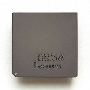
80376Intel 80376The Intel 80376, introduced January 16, 1989, was a variant of the Intel 80386SX intended for embedded systems.It differed from the 80386 in not supporting real mode and having no support for paging in the MMU...
- Introduced January 16, 1989; Discontinued June 15, 2001
- Variant of 386SX intended for embedded systems
- No "real mode", starts up directly in "protected mode"
- Replaced by much more successful 80386EX from 1994
80860 (i860) (chronological entry)
- Introduced February 27, 1989
- See main entry
80486DX (chronological entry)
- Introduced April 10, 1989
- See main entry
80386SL
- Introduced October 15, 1990
- Clock rates:
- 20 MHz with 4.21 MIPS
- 25 MHz with 5.3 MIPS, introduced September 30, 1991
- Internal architecture 32 bits
- External bus width 16 bits
- Number of Transistors 855,000 at 1 µm
- Addressable memory 4 GB
- Virtual memory 1 TB
- First chip specifically made for portable computers because of low power consumption of chip
- Highly integrated, includes cache, bus, and memory controllers
80486SX/DX2/SL, Pentium, 80486DX4 (chronological entries)
- Introduced 1991–1994
- See main entries
80386EXIntel 80386EXThe Intel 80386EX is a variant of the Intel 386 microprocessor designed for embedded systems. Introduced in August 1994 and was successful in the market being used aboard several orbiting satellites and microsatellites....
- Introduced August 1994
- Variant of 80386SX intended for embedded systemEmbedded systemAn embedded system is a computer system designed for specific control functions within a larger system. often with real-time computing constraints. It is embedded as part of a complete device often including hardware and mechanical parts. By contrast, a general-purpose computer, such as a personal...
s - Static core, i.e. may run as slowly (and thus, power efficiently) as desired, down to full halt
- On-chip peripherals:
- Clock and power mgmt
- Timers/counters
- Watchdog timerWatchdog timerA watchdog timer is a computer hardware or software timer that triggers a system reset or other corrective action if the main program, due to some fault condition, such as a hang, neglects to regularly service the watchdog A watchdog timer (or computer operating properly (COP) timer) is a computer...
- Serial I/O units (sync and async) and parallel I/O
- DMADirect memory accessDirect memory access is a feature of modern computers that allows certain hardware subsystems within the computer to access system memory independently of the central processing unit ....
- RAM refresh
- JTAGJTAGJoint Test Action Group is the common name for what was later standardized as the IEEE 1149.1 Standard Test Access Port and Boundary-Scan Architecture. It was initially devised for testing printed circuit boards using boundary scan and is still widely used for this application.Today JTAG is also...
test logic
- Significantly more successful than the 80376
- Used aboard several orbiting satellites and microsatellites
- Used in NASA's FlightLinux project
80486DX
- Introduced April 10, 1989
- Clock rates:
- 25 MHz with 20 MIPS (16.8 SPECint92, 7.40 SPECfp92)
- 33 MHz with 27 MIPS (22.4 SPECint92 on Micronics M4P 128 KB L2), introduced May 7, 1990
- 50 MHz with 41 MIPS (33.4 SPECint92, 14.5 SPECfp92 on Compaq/50L 256 KB L2), introduced June 24, 1991
- Bus Width 32 bits
- Number of Transistors 1.2 million at 1 µm; the 50 MHz was at 0.8 µm
- Addressable memory 4 GB
- Virtual memory 1 TB
- Level 1 cache of 8 KB on chip
- Math coprocessor on chip
- 50X performance of the 8088
- Used in Desktop computing and servers
- Family 4 model 3
80386SL (chronological entry)
- Introduced October 15, 1990
- See main entry
80486SXIntel 80486SXThe Intel's i486SX was a modified Intel 486DX microprocessor with its floating-point unit disconnected. All early 486SX chips were actually i486DX chips with a defective FPU...
- Introduced April 22, 1991
- Clock rates:
- 16 MHz with 13 MIPS
- 20 MHz with 16.5 MIPS, introduced September 16, 1991
- 25 MHz with 20 MIPS (12 SPECint92), introduced September 16, 1991
- 33 MHz with 27 MIPS (15.86 SPECint92), introduced September 21, 1992
- Bus Width 32 bits
- Number of Transistors 1.185 million at 1 µm and 900,000 at 0.8 µm
- Addressable memory 4 GB
- Virtual memory 1 TB
- Identical in design to 486DX but without math coprocessor. The first version was an 80486DX with disabled mathco in the chip and different pin configuration. If the user needed math co capabilities, he must add 487SX which was actually an 486DX with different pin configuration to prevent the user from installing a 486DX instead of 487SX, so with this configuration 486SX+487SX you had 2 identical CPU's with only 1 turned on
- Used in low-cost entry to 486 CPU desktop computing
- Upgradable with the Intel OverDrive processorIntel 80486 OverDriveThe Intel's i486 OverDrive processors are a category of various Intel 80486s that were produced with the designated purpose of being used to upgrade personal computers. The OverDrives typically possessed qualities different from 'standard' i486s with the same speed steppings...
- Family 4 model 2
80486DX2Intel 80486DX2The Intel 80486DX2 is a CPU produced by Intel that was introduced in 1992. The i486DX2 was nearly identical to the i486DX but for the addition of clock multiplier circuitry. It was the first chip to use clock doubling, whereby the processor runs two internal logic clock cycles per external bus cycle...
- Introduced March 3, 1992
Runs at twice the speed of the external bus (FSB).
- Clock rates:
- 40 MHz
- 50 MHz
- 66 MHz
- 100 MHz (This was only made a short time due to high failure rates.)
80486SLIntel 80486SLThe Intel's i486SL is the power-saving variant of the i486DX microprocessor. The SL was designed for use in mobile computers. It was produced between November 1992 and June 1993. Clock speeds available were 20, 25 and 33 MHz...
- Introduced November 9, 1992
- Clock rates:
- 20 MHz with 15.4MIPS
- 25 MHz with 19 MIPS
- 33 MHz with 25 MIPS
- Bus Width 32 bits
- Number of Transistors 1.4 million at 0.8 µm
- Addressable memory 4 GB
- Virtual memory 1 TB
- Used in notebook computers
- Family 4 model 3
Pentium (chronological entry)
- Introduced March 22, 1993
- See main entry
80486DX4Intel 80486DX4The IntelDX4 is a clock-tripled i486 microprocessor with 16 kB L1 cache. Intel named it DX4 as a consequence of litigation with AMD over trademarks...
- Introduced March 7, 1994
- Clock rates:
- 75 MHz with 53 MIPS (41.3 SPECint92, 20.1 SPECfp92 on Micronics M4P 256 KB L2)
- 100 MHz with 70.7 MIPS (54.59 SPECint92, 26.91 SPECfp92 on Micronics M4P 256 KB L2)
- Number of Transistors 1.6 million at 0.6 µm
- Bus width 32 bits
- Addressable memory 4 GB
- Virtual memory 64 TB
- Pin count 168 PGA PackagePin grid arrayA pin grid array, often abbreviated PGA, is a type of integrated circuit packaging. In a PGA, the package is square or roughly square, and the pins are arranged in a regular array on the underside of the package...
, 208 sq ftPQFPA QFP or Quad Flat Package is a surface mount integrated circuit package with leads extending from each of the four sides. Socketing such packages is rare and hole mounting is not possible. Versions ranging from 32 to 304 pins with a pitch ranging from 0.4 to 1.0 mm are common...
Package - Used in high performance entry-level desktops and value notebooks
- Family 4 model 8
Original Pentium
- Bus width 64 bits
- System bus clock rate 60 or 66 MHz
- Address bus 32 bits
- Addressable Memory 4 GB
- Virtual Memory 64 TB
- SuperscalarSuperscalarA superscalar CPU architecture implements a form of parallelism called instruction level parallelism within a single processor. It therefore allows faster CPU throughput than would otherwise be possible at a given clock rate...
architecture - Runs on 5 volts
- Used in desktops
- 8 KB of instruction cacheCPU cacheA CPU cache is a cache used by the central processing unit of a computer to reduce the average time to access memory. The cache is a smaller, faster memory which stores copies of the data from the most frequently used main memory locations...
- 8 KB of data cache
- P5 – 0.8 µm process technology800 nanometerThe 800 nm process refers to the level of semiconductor process technology that was reached in the 1989–1990 timeframe, by most leading semiconductor companies, like Intel and IBM.-Products featuring 0.8 µm manufacturing process:...
- Introduced March 22, 1993
- Number of transistors 3.1 million
- Socket 4Socket 4Socket 4, presented in 1993, was the first CPU socket designed for the early P5 Pentium microprocessors. Socket 4 was the only 5-volt socket for the Pentium. After Socket 4, Intel switched to the 3.3-volt-powered Socket 5. Socket 4 does support a special Pentium OverDrive, which allows running at...
273 pin PGA processor package - Package dimensions 2.16" × 2.16"
- Family 5 model 1
- Variants
- 60 MHz with 100 MIPS (70.4 SPECint92, 55.1 SPECfp92 on Xpress 256 KB L2)
- 66 MHz with 112 MIPS (77.9 SPECint92, 63.6 SPECfp92 on Xpress 256 KB L2)
- P54 – 0.6 µm process technology600 nanometerThe 600 nm process refers to the level of semiconductor process technology that was reached in the 1994–1995 timeframe, by most leading semiconductor companies, like Intel and IBM.-Products featuring 0.6 µm manufacturing process:...
- Socket 5Socket 5Socket 5 was created for the second generation of Intel P5 Pentium processors operating at speeds from 75 to 120 MHz as well as certain Pentium OverDrive and Pentium MMX processors with core voltage 3.3 V. Consisting of 320 pins, this was the first socket to use a staggered pin grid array, or...
296/320 pin PGA package - Number of transistors 3.2 million
- Variants
- 75 MHz Introduced October 10, 1994
- 90, 100 MHz Introduced March 7, 1994
- Socket 5
- P54CQS – 0.35 µm process technology350 nanometerThe 350 nm process refers to the level of semiconductor process technology that was reached in the 1995–1996 timeframe, by most leading semiconductor companies, like Intel and IBM.-Products featuring 350 nm manufacturing process:...
- Socket 5Socket 5Socket 5 was created for the second generation of Intel P5 Pentium processors operating at speeds from 75 to 120 MHz as well as certain Pentium OverDrive and Pentium MMX processors with core voltage 3.3 V. Consisting of 320 pins, this was the first socket to use a staggered pin grid array, or...
296/320 pin PGA package - Number of transistors 3.2 million
- Variants
- 120 MHz Introduced March 27, 1995
- Socket 5
- P54CS – 0.35 µm process technology350 nanometerThe 350 nm process refers to the level of semiconductor process technology that was reached in the 1995–1996 timeframe, by most leading semiconductor companies, like Intel and IBM.-Products featuring 350 nm manufacturing process:...
- Number of transistors 3.3 million
- 90 mm² die size
- Family 5 model 2
- Variants
- Socket 5Socket 5Socket 5 was created for the second generation of Intel P5 Pentium processors operating at speeds from 75 to 120 MHz as well as certain Pentium OverDrive and Pentium MMX processors with core voltage 3.3 V. Consisting of 320 pins, this was the first socket to use a staggered pin grid array, or...
296/320 pin PGA package- 133 MHz Introduced June 12, 1995
- 150, 166 MHz Introduced January 4, 1996
- Socket 7Socket 7Socket 7 is a physical and electrical specification for an x86-style CPU socket on a personal computer motherboard. The socket supersedes the earlier Socket 5, and accepts P5 Pentium microprocessors manufactured by Intel, as well as compatibles made by Cyrix/IBM, AMD, IDT and others.Socket 7 was...
296/321 pin PGA package- 200 MHz Introduced June 10, 1996
Pentium with MMX Technology
- P55C – 0.35 µm process technology350 nanometerThe 350 nm process refers to the level of semiconductor process technology that was reached in the 1995–1996 timeframe, by most leading semiconductor companies, like Intel and IBM.-Products featuring 350 nm manufacturing process:...
- Introduced January 8, 1997
- Intel MMX (instruction set) support
- Socket 7Socket 7Socket 7 is a physical and electrical specification for an x86-style CPU socket on a personal computer motherboard. The socket supersedes the earlier Socket 5, and accepts P5 Pentium microprocessors manufactured by Intel, as well as compatibles made by Cyrix/IBM, AMD, IDT and others.Socket 7 was...
296/321 pin PGA (pin grid array) package - 16 KB L1 instruction cache
- 16 KB L1 data cache
- Number of transistors 4.5 million
- System bus clock rate 66 MHz
- Basic P55C is family 5 model 4, mobile are family 5 model 7 and 8
- Variants
- 166, 200 MHz Introduced January 8, 1997
- 233 MHz Introduced June 2, 1997
- 133 MHz (Mobile)
- 166, 266 MHz (Mobile) Introduced January 12, 1998
- 200, 233 MHz (Mobile) Introduced September 8, 1997
- 300 MHz (Mobile) Introduced January 7, 1999
32-bit processors: P6P6 (microarchitecture)The P6 microarchitecture is the sixth generation Intel x86 microarchitecture, implemented by the Pentium Pro microprocessor that was introduced in November 1995. It is sometimes referred to as i686. It was succeeded by the NetBurst microarchitecture in 2000, but eventually revived in the Pentium M...
/Pentium M microarchitecture
Pentium ProPentium ProThe Pentium Pro is a sixth-generation x86 microprocessor developed and manufactured by Intel introduced in November 1, 1995 . It introduced the P6 microarchitecture and was originally intended to replace the original Pentium in a full range of applications...
- Introduced November 1, 1995
- Precursor to Pentium II and III
- Primarily used in server systems
- Socket 8Socket 8The Socket 8 CPU socket was used exclusively with the Intel Pentium Pro and Pentium II Overdrive computer processors. Intel discontinued Socket 8 in favor of Slot 1 with the introduction of the Pentium II.-Technical specifications:...
processor package (387 pins) (Dual SPGA) - Number of transistors 5.5 million
- Family 6 model 1
- 0.6 µm process technology600 nanometerThe 600 nm process refers to the level of semiconductor process technology that was reached in the 1994–1995 timeframe, by most leading semiconductor companies, like Intel and IBM.-Products featuring 0.6 µm manufacturing process:...
- 16 KB L1 cache
- 256 KB integrated L2 cache
- 60 MHz system bus clock rate
- Variants
- 150 MHz
- 0.35 µm process technology350 nanometerThe 350 nm process refers to the level of semiconductor process technology that was reached in the 1995–1996 timeframe, by most leading semiconductor companies, like Intel and IBM.-Products featuring 350 nm manufacturing process:...
, or 0.35 µm CPU with 0.6 µm L2 cache- Number of transistors 5.5 million
- 512 KB or 256 KB integrated L2 cache
- 60 or 66 MHz system bus clock rate
- Variants
- 166 MHz (66 MHz bus clock rate, 512 KB 0.35 µm cache) Introduced November 1, 1995
- 180 MHz (60 MHz bus clock rate, 256 KB 0.6 µm cache) Introduced November 1, 1995
- 200 MHz (66 MHz bus clock rate, 256 KB 0.6 µm cache) Introduced November 1, 1995
- 200 MHz (66 MHz bus clock rate, 512 KB 0.35 µm cache) Introduced November 1, 1995
- 200 MHz (66 MHz bus clock rate, 1 MB 0.35 µm cache) Introduced August 18, 1997
Pentium IIPentium IIThe Pentium II brand refers to Intel's sixth-generation microarchitecture and x86-compatible microprocessors introduced on May 7, 1997. Containing 7.5 million transistors, the Pentium II featured an improved version of the first P6-generation core of the Pentium Pro, which contained 5.5 million...
- Introduced May 7, 1997
- Pentium Pro with MMX and improved 16-bit performance
- 242-pin Slot 1Slot 1Slot 1 refers to the physical and electrical specification for the connector used by some of Intel's microprocessors, including the Pentium Pro, Celeron, Pentium II and the Pentium III...
(SEC) processor package - Slot 1
- Number of transistors 7.5 million
- 32 KB L1 cache
- 512 KB ½ bandwidth external L2 cache
- The only Pentium II that did not have the L2 cache at ½ bandwidth of the core was the Pentium II 450 PE.
- Klamath – 0.35 µm process technology350 nanometerThe 350 nm process refers to the level of semiconductor process technology that was reached in the 1995–1996 timeframe, by most leading semiconductor companies, like Intel and IBM.-Products featuring 350 nm manufacturing process:...
(233, 266, 300 MHz)- 66 MHz system bus clock rate
- Family 6 model 3
- Variants
- 233, 266, 300 MHz Introduced May 7, 1997
- Deschutes – 0.25 µm process technology250 nanometerThe 250 nm process refers to a level of semiconductor process technology.-Products featuring 250 nm manufacturing process:*The DEC Alpha 21264A, which was made commercially available in 1999.*The AMD K6-2 Chomper and Chomper Extended...
(333, 350, 400, 450 MHz)- Introduced January 26, 1998
- 66 MHz system bus clock rate (333 MHz variant), 100 MHz system bus clock rate for all models after
- Family 6 model 5
- Variants
- 333 MHz Introduced January 26, 1998
- 350, 400 MHz Introduced April 15, 1998
- 450 MHz Introduced August 24, 1998
- 233, 266 MHz (Mobile) Introduced April 2, 1998
- 333 MHz Pentium II Overdrive processor for Socket 8 Introduced August 10, 1998; Engineering Sample Photo
- 300 MHz (Mobile) Introduced September 9, 1998
- 333 MHz (Mobile)
CeleronCeleronCeleron is a brand name given by Intel Corp. to a number of different x86 computer microprocessor models targeted at budget personal computers....
(Pentium II-based)
- Covington – 0.25 µm process technology250 nanometerThe 250 nm process refers to a level of semiconductor process technology.-Products featuring 250 nm manufacturing process:*The DEC Alpha 21264A, which was made commercially available in 1999.*The AMD K6-2 Chomper and Chomper Extended...
- Introduced April 15, 1998
- 242-pin Slot 1Slot 1Slot 1 refers to the physical and electrical specification for the connector used by some of Intel's microprocessors, including the Pentium Pro, Celeron, Pentium II and the Pentium III...
SEPP (Single Edge Processor Package) - Number of transistors 7.5 million
- 66 MHz system bus clock rate
- Slot 1
- 32 KB L1 cache
- No L2 cache
- Variants
- 266 MHz Introduced April 15, 1998
- 300 MHz Introduced June 9, 1998
- Mendocino – 0.25 µm process technology250 nanometerThe 250 nm process refers to a level of semiconductor process technology.-Products featuring 250 nm manufacturing process:*The DEC Alpha 21264A, which was made commercially available in 1999.*The AMD K6-2 Chomper and Chomper Extended...
- Introduced August 24, 1998
- 242-pin Slot 1Slot 1Slot 1 refers to the physical and electrical specification for the connector used by some of Intel's microprocessors, including the Pentium Pro, Celeron, Pentium II and the Pentium III...
SEPP (Single Edge Processor Package), Socket 370Socket 370Socket 370 is a common format of CPU socket first used by Intel for Pentium III and Celeron processors to replace the older Slot 1 CPU interface on personal computers. The "370" refers to the number of pin holes in the socket for CPU pins...
PPGA package - Number of transistors 19 million
- 66 MHz system bus clock rate
- Slot 1, Socket 370
- 32 KB L1 cache
- 128 KB integrated cache
- Family 6 model 6
- Variants
- 300, 333 MHz Introduced August 24, 1998
- 366, 400 MHz Introduced January 4, 1999
- 433 MHz Introduced March 22, 1999
- 466 MHz
- 500 MHz Introduced August 2, 1999
- 533 MHz Introduced January 4, 2000
- 266 MHz (Mobile)
- 300 MHz (Mobile)
- 333 MHz (Mobile) Introduced April 5, 1999
- 366 MHz (Mobile)
- 400 MHz (Mobile)
- 433 MHz (Mobile)
- 450 MHz (Mobile) Introduced February 14, 2000
- 466 MHz (Mobile)
- 500 MHz (Mobile) Introduced February 14, 2000
Pentium II Xeon (chronological entry)
- Introduced June 29, 1998
- See main entry
Pentium IIIPentium IIIThe Pentium III brand refers to Intel's 32-bit x86 desktop and mobile microprocessors based on the sixth-generation P6 microarchitecture introduced on February 26, 1999. The brand's initial processors were very similar to the earlier Pentium II-branded microprocessors...
- Katmai – 0.25 µm process technology250 nanometerThe 250 nm process refers to a level of semiconductor process technology.-Products featuring 250 nm manufacturing process:*The DEC Alpha 21264A, which was made commercially available in 1999.*The AMD K6-2 Chomper and Chomper Extended...
- Introduced February 26, 1999
- Improved PII, i.e. P6-based core, now including Streaming SIMD ExtensionsStreaming SIMD ExtensionsIn computing, Streaming SIMD Extensions is a SIMD instruction set extension to the x86 architecture, designed by Intel and introduced in 1999 in their Pentium III series processors as a reply to AMD's 3DNow! . SSE contains 70 new instructions, most of which work on single precision floating point...
(SSE) - Number of transistors 9.5 million
- 512 KB ½ bandwidth L2 External cache
- 242-pin Slot 1Slot 1Slot 1 refers to the physical and electrical specification for the connector used by some of Intel's microprocessors, including the Pentium Pro, Celeron, Pentium II and the Pentium III...
SECC2 (Single Edge Contact cartridge 2) processor package - System Bus clock rate 100 MHz, 133 MHz (B-models)
- Slot 1
- Family 6 model 7
- Variants
- 450, 500 MHz Introduced February 26, 1999
- 550 MHz Introduced May 17, 1999
- 600 MHz Introduced August 2, 1999
- 533, 600 MHz Introduced (133 MHz bus clock rate) September 27, 1999
- Coppermine – 0.18 µm process technology180 nanometerThe 180 nm process refers to the level of semiconductor process technology that was reached in the 1999–2000 timeframe, by most leading semiconductor companies, like Intel, Texas Instruments, IBM, and TSMC....
- Introduced October 25, 1999
- Number of transistors 28.1 million
- 256 KB Advanced Transfer L2 Cache (Integrated)
- 242-pin Slot-1 SECC2 (Single Edge Contact cartridge 2) processor package, 370-pin FC-PGA (Flip-chip pin grid array) package
- System Bus clock rate 100 MHz (E-models), 133 MHz (EB models)
- Slot 1, Socket 370
- Family 6 model 8
- Variants
- 500 MHz (100 MHz bus clock rate)
- 533 MHz
- 550 MHz (100 MHz bus clock rate)
- 600 MHz
- 600 MHz (100 MHz bus clock rate)
- 650 MHz (100 MHz bus clock rate) Introduced October 25, 1999
- 667 MHz Introduced October 25, 1999
- 700 MHz (100 MHz bus clock rate) Introduced October 25, 1999
- 733 MHz Introduced October 25, 1999
- 750, 800 MHz (100 MHz bus clock rate) Introduced December 20, 1999
- 850 MHz (100 MHz bus clock rate) Introduced March 20, 2000
- 866 MHz Introduced March 20, 2000
- 933 MHz Introduced May 24, 2000
- 1000 MHz Introduced March 8, 2000 (Not widely available at time of release)
- 1100 MHz
- 1133 MHz (first version recalled, later re-released)
- 400, 450, 500 MHz (Mobile) Introduced October 25, 1999
- 600, 650 MHz (Mobile) Introduced January 18, 2000
- 700 MHz (Mobile) Introduced April 24, 2000
- 750 MHz (Mobile) Introduced June 19, 2000
- 800, 850 MHz (Mobile) Introduced September 25, 2000
- 900, 1000 MHz (Mobile) Introduced March 19, 2001
- Tualatin – 0.13 µm process technology130 nanometerThe 130 nm process refers to the level of semiconductor process technology that was reached in the 2000–2001 timeframe, by most leading semiconductor companies, like Intel, Texas Instruments, IBM, and TSMC....
- Introduced July 2001
- Number of transistors 28.1 million
- 32 KB L1 cache
- 256 KB or 512 KB Advanced Transfer L2 cache (Integrated)
- 370-pin FC-PGA2 (Flip-chip pin grid array) package
- 133 MHz system bus clock rate
- Socket 370
- Family 6 model 11
- Variants
- 1133 MHz (256 KB L2)
- 1133 MHz (512 KB L2)
- 1200 MHz
- 1266 MHz (512 KB L2)
- 1333 MHz
- 1400 MHz (512 KB L2)
Pentium II and III XeonXeonThe Xeon is a brand of multiprocessing- or multi-socket-capable x86 microprocessors from Intel Corporation targeted at the non-consumer server, workstation and embedded system markets.-Overview:...
- PII Xeon
- Variants
- 400 MHz Introduced June 29, 1998
- 450 MHz (512 KB L2 Cache) Introduced October 6, 1998
- 450 MHz (1 MB and 2 MB L2 Cache) Introduced January 5, 1999
- Variants
- PIII Xeon
- Introduced October 25, 1999
- Number of transistors: 9.5 million at 0.25 µm or 28 million at 0.18 µm
- L2 cache is 256 KB, 1 MB, or 2 MB Advanced Transfer Cache (Integrated)
- Processor Package Style is Single Edge Contact Cartridge (S.E.C.C.2) or SC330
- System Bus clock rate 133 MHz (256 KB L2 cache) or 100 MHz (1 – 2 MB L2 cache)
- System Bus Width 64 bit
- Addressable memory 64 GB
- Used in two-way servers and workstations (256 KB L2) or 4- and 8-way servers (1 – 2 MB L2)
- Family 6 model 10
- Variants
- 500 MHz (0.25 µm process250 nanometerThe 250 nm process refers to a level of semiconductor process technology.-Products featuring 250 nm manufacturing process:*The DEC Alpha 21264A, which was made commercially available in 1999.*The AMD K6-2 Chomper and Chomper Extended...
) Introduced March 17, 1999 - 550 MHz (0.25 µm process) Introduced August 23, 1999
- 600 MHz (0.18 µm process180 nanometerThe 180 nm process refers to the level of semiconductor process technology that was reached in the 1999–2000 timeframe, by most leading semiconductor companies, like Intel, Texas Instruments, IBM, and TSMC....
, 256 KB L2 cache) Introduced October 25, 1999 - 667 MHz (0.18 µm process, 256 KB L2 cache) Introduced October 25, 1999
- 733 MHz (0.18 µm process, 256 KB L2 cache) Introduced October 25, 1999
- 800 MHz (0.18 µm process, 256 KB L2 cache) Introduced January 12, 2000
- 866 MHz (0.18 µm process, 256 KB L2 cache) Introduced April 10, 2000
- 933 MHz (0.18 µm process, 256 KB L2 cache)
- 1000 MHz (0.18 µm process, 256 KB L2 cache) Introduced August 22, 2000
- 700 MHz (0.18 µm process, 1 – 2 MB L2 cache) Introduced May 22, 2000
- 500 MHz (0.25 µm process
CeleronCeleronCeleron is a brand name given by Intel Corp. to a number of different x86 computer microprocessor models targeted at budget personal computers....
(Pentium III Coppermine-based)
- Coppermine-128, 0.18 µm process technology
- Introduced March, 2000
- Streaming SIMD ExtensionsStreaming SIMD ExtensionsIn computing, Streaming SIMD Extensions is a SIMD instruction set extension to the x86 architecture, designed by Intel and introduced in 1999 in their Pentium III series processors as a reply to AMD's 3DNow! . SSE contains 70 new instructions, most of which work on single precision floating point...
(SSE) - Socket 370Socket 370Socket 370 is a common format of CPU socket first used by Intel for Pentium III and Celeron processors to replace the older Slot 1 CPU interface on personal computers. The "370" refers to the number of pin holes in the socket for CPU pins...
, FC-PGA processor package - Number of transistors 28.1 million
- 66 MHz system bus clock rate, 100 MHz system bus clock rate from January 3, 2001
- 32 kB L1 cache
- 128 kB Advanced Transfer L2 cache
- Family 6 model 8
- Variants
- 533 MHz
- 566 MHz
- 600 MHz
- 633, 667, 700 MHz Introduced June 26, 2000
- 733, 766 MHz Introduced November 13, 2000
- 800 MHz Introduced January 3, 2001
- 850 MHz Introduced April 9, 2001
- 900 MHz Introduced July 2, 2001
- 950, 1000, 1100 MHz Introduced August 31, 2001
- 550 MHz (Mobile)
- 600, 650 MHz (Mobile) Introduced June 19, 2000
- 700 MHz (Mobile) Introduced September 25, 2000
- 750 MHz (Mobile) Introduced March 19, 2001
- 800 MHz (Mobile)
- 850 MHz (Mobile) Introduced July 2, 2001
- 600 MHz (LV Mobile)
- 500 MHz (ULV Mobile) Introduced January 30, 2001
- 600 MHz (ULV Mobile)
XScale (chronological entry)
- Introduced August 23, 2000
- See main entry
Pentium 4 (not 4EE, 4E, 4F), Itanium, P4-based Xeon, Itanium 2 (chronological entries)
- Introduced April 2000 – July 2002
- See main entries
CeleronCeleronCeleron is a brand name given by Intel Corp. to a number of different x86 computer microprocessor models targeted at budget personal computers....
(Pentium III Tualatin-based)
- Tualatin Celeron – 0.13 µm process technology130 nanometerThe 130 nm process refers to the level of semiconductor process technology that was reached in the 2000–2001 timeframe, by most leading semiconductor companies, like Intel, Texas Instruments, IBM, and TSMC....
- 32 KB L1 cache
- 256 KB Advanced Transfer L2 cache
- 100 MHz system bus clock rate
- Socket 370
- Family 6 model 11
- Variants
- 1.0 GHz
- 1.1 GHz
- 1.2 GHz
- 1.3 GHz
- 1.4 GHz
Pentium MPentium MThe Pentium M brand refers to a family of mobile single-core x86 microprocessors introduced in March 2003 , and forming a part of the Intel Carmel notebook platform under the then new Centrino brand...
- Banias 0.13 µm process technology130 nanometerThe 130 nm process refers to the level of semiconductor process technology that was reached in the 2000–2001 timeframe, by most leading semiconductor companies, like Intel, Texas Instruments, IBM, and TSMC....
- Introduced March 2003
- 64 KB L1 cache
- 1 MB L2 cache (integrated)
- Based on Pentium III core, with SSE2SSE2SSE2, Streaming SIMD Extensions 2, is one of the Intel SIMD processor supplementary instruction sets first introduced by Intel with the initial version of the Pentium 4 in 2001. It extends the earlier SSE instruction set, and is intended to fully supplant MMX. Intel extended SSE2 to create SSE3...
SIMD instructions and deeper pipeline - Number of transistors 77 million
- Micro-FCPGA, Micro-FCBGAMicro-FCBGAMicro-FCBGA is Intel's current BGA mounting method for mobile processors that use a flip chip binding technology. It was introduced with the Coppermine Mobile Celeron and replaces the older BGA2 ball-grid-array mounting method used in the Coppermine Pentium III mobile CPUs...
processor package - Heart of the Intel mobile CentrinoCentrinoThe Centrino brand represents Intel Wi-Fi and WiMAX adapters. It was formerly a platform-marketing initiative from Intel until January 7, 2010....
system - 400 MHz Netburst-style system bus
- Family 6 model 9
- Variants
- 900 MHz (Ultra low voltage)
- 1.0 GHz (Ultra low voltage)
- 1.1 GHz (Low voltage)
- 1.2 GHz (Low voltage)
- 1.3 GHz
- 1.4 GHz
- 1.5 GHz
- 1.6 GHz
- 1.7 GHz
- Dothan 0.09 µm (90 nm90 nanometerThe 90 nm process refers to the level of CMOS process technology that was reached in the 2002–2003 timeframe, by most leading semiconductor companies, like Intel, AMD, Infineon, Texas Instruments, IBM, and TSMC....
) process technology- Introduced May 2004
- 2 MB L2 cache
- 140 million transistors
- Revised data prefetch unit
- 400 MHz Netburst-style system bus
- 21W TDPThermal Design PowerThe thermal design power , sometimes called thermal design point, refers to the maximum amount of power the cooling system in a computer is required to dissipate. For example, a laptop's CPU cooling system may be designed for a 20 watt TDP, which means that it can dissipate up to 20 watts of heat...
- Family 6 model 13
- Variants
- 1.00 GHz (Pentium M 723) (Ultra low voltage, 5W TDP)
- 1.10 GHz (Pentium M 733) (Ultra low voltage, 5W TDP)
- 1.20 GHz (Pentium M 753) (Ultra low voltage, 5W TDP)
- 1.30 GHz (Pentium M 718) (Low voltage, 10W TDP)
- 1.40 GHz (Pentium M 738) (Low voltage, 10W TDP)
- 1.50 GHz (Pentium M 758) (Low voltage, 10W TDP)
- 1.60 GHz (Pentium M 778) (Low voltage, 10W TDP)
- 1.40 GHz (Pentium M 710)
- 1.50 GHz (Pentium M 715)
- 1.60 GHz (Pentium M 725)
- 1.70 GHz (Pentium M 735)
- 1.80 GHz (Pentium M 745)
- 2.00 GHz (Pentium M 755)
- 2.10 GHz (Pentium M 765)
- Dothan 533 0.09 µm (90 nm90 nanometerThe 90 nm process refers to the level of CMOS process technology that was reached in the 2002–2003 timeframe, by most leading semiconductor companies, like Intel, AMD, Infineon, Texas Instruments, IBM, and TSMC....
) process technology- Introduced Q1 2005
- Same as Dothan except with a 533 MHz NetBurst-style system bus and 27W TDPThermal Design PowerThe thermal design power , sometimes called thermal design point, refers to the maximum amount of power the cooling system in a computer is required to dissipate. For example, a laptop's CPU cooling system may be designed for a 20 watt TDP, which means that it can dissipate up to 20 watts of heat...
- Variants
- 1.60 GHz (Pentium M 730)
- 1.73 GHz (Pentium M 740)
- 1.86 GHz (Pentium M 750)
- 2.00 GHz (Pentium M 760)
- 2.13 GHz (Pentium M 770)
- 2.26 GHz (Pentium M 780)
- Stealey 0.09 µm (90 nm90 nanometerThe 90 nm process refers to the level of CMOS process technology that was reached in the 2002–2003 timeframe, by most leading semiconductor companies, like Intel, AMD, Infineon, Texas Instruments, IBM, and TSMC....
) process technology- Introduced Q2 2007
- 512 KB L2, 3W TDP
- Variants
- 600 MHz (A100)
- 800 MHz (A110)
Celeron MCeleronCeleron is a brand name given by Intel Corp. to a number of different x86 computer microprocessor models targeted at budget personal computers....
- Banias-512 0.13 µm130 nanometerThe 130 nm process refers to the level of semiconductor process technology that was reached in the 2000–2001 timeframe, by most leading semiconductor companies, like Intel, Texas Instruments, IBM, and TSMC....
process technology- Introduced March 2003
- 64 KB L1 cache
- 512 KB L2 cache (integrated)
- SSE2SSE2SSE2, Streaming SIMD Extensions 2, is one of the Intel SIMD processor supplementary instruction sets first introduced by Intel with the initial version of the Pentium 4 in 2001. It extends the earlier SSE instruction set, and is intended to fully supplant MMX. Intel extended SSE2 to create SSE3...
SIMD instructions - No SpeedStepSpeedStepSpeedStep is a trademark for a series of dynamic frequency scaling technologies built into some Intel microprocessors that allow the clock speed of the processor to be dynamically changed by software...
technology, is not part of the 'CentrinoCentrinoThe Centrino brand represents Intel Wi-Fi and WiMAX adapters. It was formerly a platform-marketing initiative from Intel until January 7, 2010....
' package - Family 6 model 9
- Variants
- 310 – 1.20 GHz
- 320 – 1.30 GHz
- 330 – 1.40 GHz
- 340 – 1.50 GHz
- Dothan-1024 90 nm90 nanometerThe 90 nm process refers to the level of CMOS process technology that was reached in the 2002–2003 timeframe, by most leading semiconductor companies, like Intel, AMD, Infineon, Texas Instruments, IBM, and TSMC....
process technology- 64 KB L1 cache
- 1 MB L2 cache (integrated)
- SSE2SSE2SSE2, Streaming SIMD Extensions 2, is one of the Intel SIMD processor supplementary instruction sets first introduced by Intel with the initial version of the Pentium 4 in 2001. It extends the earlier SSE instruction set, and is intended to fully supplant MMX. Intel extended SSE2 to create SSE3...
SIMD instructions - No SpeedStep technology, is not part of the 'CentrinoCentrinoThe Centrino brand represents Intel Wi-Fi and WiMAX adapters. It was formerly a platform-marketing initiative from Intel until January 7, 2010....
' package - Variants
- 350 – 1.30 GHz
- 350J – 1.30 GHz, with Execute Disable bit
- 360 – 1.40 GHz
- 360J – 1.40 GHz, with Execute Disable bit
- 370 – 1.50 GHz, with Execute Disable bit
- Family 6, Model 13, Stepping 8
- 380 – 1.60 GHz, with Execute Disable bit
- 390 – 1.70 GHz, with Execute Disable bit
- Yonah-1024 65 nm65 nanometerThe 65 nm process is an advanced lithographic node used in volume CMOS semiconductor fabrication. Printed linewidths can reach as low as 25 nm on a nominally 65 nm process, while the pitch between two lines may be greater than 130 nm.. For comparison, cellular ribosomes are...
process technology- 64 KB L1 cache
- 1 MB L2 cache (integrated)
- SSE3SSE3SSE3, Streaming SIMD Extensions 3, also known by its Intel code name Prescott New Instructions , is the third iteration of the SSE instruction set for the IA-32 architecture. Intel introduced SSE3 in early 2004 with the Prescott revision of their Pentium 4 CPU...
SIMD instructions, 533 MHz front-side bus, execute-disable bit - No SpeedStep technology, is not part of the 'CentrinoCentrinoThe Centrino brand represents Intel Wi-Fi and WiMAX adapters. It was formerly a platform-marketing initiative from Intel until January 7, 2010....
' package - Variants
- 410 – 1.46 GHz
- 420 – 1.60 GHz,
- 423 – 1.06 GHz (ultra low voltage)
- 430 – 1.73 GHz
- 440 – 1.86 GHz
- 443 – 1.20 GHz (ultra low voltage)
- 450 – 2.00 GHz
Intel CoreIntel CoreYonah was the code name for Intel's first generation of 65 nm process mobile microprocessors, based on the Banias/Dothan-core Pentium M microarchitecture. SIMD performance has been improved through the addition of SSE3 instructions and improvements to SSE and SSE2 implementations, while integer...
- Yonah 0.065 µm (65 nm) process technology
- Introduced January 2006
- 533/667 MHz front side busFront side busA front-side bus is a computer communication interface often used in computers during the 1990s and 2000s.It typically carries data between the central processing unit and a memory controller hub, known as the northbridge....
- 2 MB (Shared on Duo) L2 cache
- SSE3SSE3SSE3, Streaming SIMD Extensions 3, also known by its Intel code name Prescott New Instructions , is the third iteration of the SSE instruction set for the IA-32 architecture. Intel introduced SSE3 in early 2004 with the Prescott revision of their Pentium 4 CPU...
SIMD instructions - 31W TDPThermal Design PowerThe thermal design power , sometimes called thermal design point, refers to the maximum amount of power the cooling system in a computer is required to dissipate. For example, a laptop's CPU cooling system may be designed for a 20 watt TDP, which means that it can dissipate up to 20 watts of heat...
(T versions) - Family 6, Model 14
- Variants:
- Intel Core Duo T2700 2.33 GHz
- Intel Core Duo T2600 2.16 GHz
- Intel Core Duo T2500 2 GHz
- Intel Core Duo T2450 2 GHz
- Intel Core Duo T2400 1.83 GHz
- Intel Core Duo T2300 1.66 GHz
- Intel Core Duo T2050 1.6 GHz
- Intel Core Duo T2300e 1.66 GHz
- Intel Core Duo T2080 1.73 GHz
- Intel Core Duo L2500 1.83 GHz (Low voltage, 15W TDPThermal Design PowerThe thermal design power , sometimes called thermal design point, refers to the maximum amount of power the cooling system in a computer is required to dissipate. For example, a laptop's CPU cooling system may be designed for a 20 watt TDP, which means that it can dissipate up to 20 watts of heat...
) - Intel Core Duo L2400 1.66 GHz (Low voltage, 15W TDP)
- Intel Core Duo L2300 1.5 GHz (Low voltage, 15W TDP)
- Intel Core Duo U2500 1.2 GHz (Ultra low voltage, 9W TDP)
- Intel Core Solo T1350 1.86 GHz (533 FSB)
- Intel Core Solo T1300 1.66 GHz
- Intel Core Solo T1200 1.5 GHz
Dual-Core XeonXeonThe Xeon is a brand of multiprocessing- or multi-socket-capable x86 microprocessors from Intel Corporation targeted at the non-consumer server, workstation and embedded system markets.-Overview:...
LV
- Sossaman 0.065 µm (65 nm) process technology
- Introduced March 2006
- Based on Yonah core, with SSE3SSE3SSE3, Streaming SIMD Extensions 3, also known by its Intel code name Prescott New Instructions , is the third iteration of the SSE instruction set for the IA-32 architecture. Intel introduced SSE3 in early 2004 with the Prescott revision of their Pentium 4 CPU...
SIMD instructions - 667 MHz frontside bus
- 2 MB Shared L2 cache
- Variants
- 2.0 GHz
Pentium 4Pentium 4Pentium 4 was a line of single-core desktop and laptop central processing units , introduced by Intel on November 20, 2000 and shipped through August 8, 2008. They had a 7th-generation x86 microarchitecture, called NetBurst, which was the company's first all-new design since the introduction of the...
- 0.18 µm process technology (1.40 and 1.50 GHz)
- Introduced November 20, 2000
- L2 cache was 256 KB Advanced Transfer Cache (Integrated)
- Processor Package Style was PGA423, PGA478
- System Bus clock rate 400 MHz
- SSE2SSE2SSE2, Streaming SIMD Extensions 2, is one of the Intel SIMD processor supplementary instruction sets first introduced by Intel with the initial version of the Pentium 4 in 2001. It extends the earlier SSE instruction set, and is intended to fully supplant MMX. Intel extended SSE2 to create SSE3...
SIMDSIMDSingle instruction, multiple data , is a class of parallel computers in Flynn's taxonomy. It describes computers with multiple processing elements that perform the same operation on multiple data simultaneously...
Extensions - Number of Transistors 42 million
- Used in desktops and entry-level workstations
- 0.18 µm process technology (1.7 GHz)
- Introduced April 23, 2001
- See the 1.4 and 1.5 chips for details
- 0.18 µm process technology (1.6 and 1.8 GHz)
- Introduced July 2, 2001
- See 1.4 and 1.5 chips for details
- Core Voltage is 1.15 volts in Maximum Performance Mode; 1.05 volts in Battery Optimized Mode
- Power <1 watt in Battery Optimized Mode
- Used in full-size and then light mobile PCs
- 0.18 µm process technology Willamette (1.9 and 2.0 GHz)
- Introduced August 27, 2001
- See 1.4 and 1.5 chips for details
- Family 15 model 1
- Pentium 4 (2 GHz, 2.20 GHz)
- Introduced January 7, 2002
- Pentium 4 (2.4 GHz)
- Introduced April 2, 2002
- 0.13 µm process technology Northwood A (1.7, 1.8, 1.9, 2, 2.2, 2.4, 2.5, 2.6, 2.8(OEM),3.0(OEM) GHz)
- Improved branch prediction and other microcodes tweaks
- 512 KB integrated L2 cache
- Number of transistors 55 million
- 400 MHz system bus.
- Family 15 model 2
- 0.13 µm process technology Northwood B (2.26, 2.4, 2.53, 2.66, 2.8, 3.06 GHz)
- 533 MHz system bus. (3.06 includes Intel's hyper threading technology).
- 0.13 µm process technology Northwood C (2.4, 2.6, 2.8, 3.0, 3.2, 3.4 GHz)
- 800 MHz system bus (all versions include Hyper Threading)
- 6500 to 10000 MIPS
Itanium (chronological entry)
- Introduced 2001
- See main entry
XeonXeonThe Xeon is a brand of multiprocessing- or multi-socket-capable x86 microprocessors from Intel Corporation targeted at the non-consumer server, workstation and embedded system markets.-Overview:...
- Official designation now Xeon, i.e. not "Pentium 4 Xeon"
- Xeon 1.4, 1.5, 1.7 GHz
- Introduced May 21, 2001
- L2 cache was 256 KB Advanced Transfer Cache (Integrated)
- Processor Package Style was Organic Land Grid Array 603 (OLGA 603)
- System Bus clock rate 400 MHz
- SSE2 SIMD Extensions
- Used in high-performance and mid-range dual processor enabled workstations
- Xeon 2.0 GHz and up to 3.6 GHz
- Introduced September 25, 2001
Itanium 2 (chronological entry)
- Introduced July 2002
- See main entry
Mobile Pentium 4-M
- 0.13 µm process technology
- 55 million transistors
- cache L2 512 KB
- BUS a 400 MHz
- Supports up to 1 GB of DDRDouble data rateIn computing, a computer bus operating with double data rate transfers data on both the rising and falling edges of the clock signal. This is also known as double pumped, dual-pumped, and double transition....
266 MHz Memory - Supports ACPIAdvanced Configuration and Power InterfaceIn computing, the Advanced Configuration and Power Interface specification provides an open standard for device configuration and power management by the operating system....
2.0 and APMAdvanced Power ManagementAdvanced power management is an API developed by Intel and Microsoft and released in 1992 which enables an operating system running an IBM-compatible personal computer to work with the BIOS to achieve power management.Revision 1.2 was the last version of the APM specification, released in 1996....
1.2 System Power Management - 1.3 V – 1.2 V (SpeedStepSpeedStepSpeedStep is a trademark for a series of dynamic frequency scaling technologies built into some Intel microprocessors that allow the clock speed of the processor to be dynamically changed by software...
) - Power: 1.2 GHz 20.8 W, 1.6 GHz 30 W, 2.6 GHz 35 W
- Sleep Power 5 W (1.2 V)
- Deeper Sleep Power = 2.9 W (1.0 V)
-
- 1.40 GHz – 23 April 2002
- 1.50 GHz – 23 April 2002
- 1.60 GHz – 4 March 2002
- 1.70 GHz – 4 March 2002
- 1.80 GHz – 23 April 2002
- 1.90 GHz – 24 June 2002
- 2.00 GHz – 24 June 2002
- 2.20 GHz – 16 September 2002
- 2.40 GHz – 14 January 2003
- 2.50 GHz – 16 April 2003
- 2.60 GHz – 11 June 2003
Pentium 4 EE
- Introduced September 2003
- EE = "Extreme Edition"
- Built from the Xeon's "Gallatin" core, but with 2 MB cache-
Pentium 4E
- Introduced February 2004
- built on 0.09 µm (90 nm90 nanometerThe 90 nm process refers to the level of CMOS process technology that was reached in the 2002–2003 timeframe, by most leading semiconductor companies, like Intel, AMD, Infineon, Texas Instruments, IBM, and TSMC....
) process technology Prescott (2.4A, 2.8, 2.8A, 3.0, 3.2, 3.4, 3.6, 3.8) 1 MB L2 cache - 533 MHz system bus (2.4A and 2.8A only)
- Number of Transistors 125 million on 1 MB Models
- Number of Transistors 169 million on 2 MB Models
- 800 MHz system bus (all other models)
- Hyper-ThreadingHyper-threadingHyper-threading is Intel's term for its simultaneous multithreading implementation in its Atom, Intel Core i3/i5/i7, Itanium, Pentium 4 and Xeon CPUs....
support is only available on CPUs using the 800 MHz system bus. - The processor's integer instruction pipeline has been increased from 20 stages to 31 stages, which theoretically allows for even greater bandwidth.
- 7500 to 11000 MIPS
- LGA 775 versions are in the 5xx series (32-bit) and 5x1 series (with Intel 64)
- The 6xx series has 2 MB L2 cache and Intel 64
Pentium 4F
- Introduced Spring 2004
- same core as 4E, "Prescott"
- 3.2–3.6 GHz
- starting with the D0 stepping of this processor, Intel 64 64-bit extensions has also been incorporated
64-bit processors: IA-64
- New instruction set, not at all related to x86.
- Before the feature was eliminated (MontecitoMontecito (processor)Montecito is the code-name of a major release of Intel's Itanium 2 Processor Family , which implements the Intel Itanium architecture on a dual-core processor. It was officially launched by Intel on July 18, 2006 as the "Dual-Core Intel Itanium 2 processor"...
, July 2006) IA-64 processors supported 32-bit x86 in hardware, but slowly (see its 2001 market reception and 2006 architectural changes).
Itanium
- Code name Merced
- Family 0x07
- Released May 29, 2001
- 733 MHz and 800 MHz
- 2MB cache
- all recalled and replaced by Itanium-II
Itanium 2
- Family 0x1F
- Released July 2002
- 900 MHz – 1.6 GHz
- McKinley 900 MHz 1.5MB cache, Model 0x0
- McKinley 1 GHz, 3MB cache, Model 0x0
- Deerfield 1 GHz, 1.5MB cache, Model 0x1
- Madison 1.3 GHz, 3MB cache, Model 0x1
- Madison 1.4 GHz, 4MB cache, Model 0x1
- Madison 1.5 GHz, 6MB cache, Model 0x1
- Madison 1.67 GHz, 9MB cache, Model 0x1
- Hondo 1.4 GHz, 4MB cache, dual core MCM, Model 0x1
64-bit processors: Intel 64 – NetBurst microarchitecture
- Intel Extended Memory 64 Technology
- Mostly compatible with AMDAdvanced Micro DevicesAdvanced Micro Devices, Inc. or AMD is an American multinational semiconductor company based in Sunnyvale, California, that develops computer processors and related technologies for commercial and consumer markets...
's AMD64 architecture - Introduced Spring 2004, with the Pentium 4F (D0 and later P4 steppings)
Pentium 4F
- Prescott-2M built on 0.09 µm (90 nm90 nanometerThe 90 nm process refers to the level of CMOS process technology that was reached in the 2002–2003 timeframe, by most leading semiconductor companies, like Intel, AMD, Infineon, Texas Instruments, IBM, and TSMC....
) process technology - 2.8–3.8 GHz (model numbers 6x0)
- Introduced February 20, 2005
- Same features as Prescott with the addition of:-
- 2 MB cache
- Intel 64bit
- Enhanced Intel SpeedStepSpeedStepSpeedStep is a trademark for a series of dynamic frequency scaling technologies built into some Intel microprocessors that allow the clock speed of the processor to be dynamically changed by software...
Technology (EIST)
- Cedar Mill built on 0.065 µm (65 nm65 nanometerThe 65 nm process is an advanced lithographic node used in volume CMOS semiconductor fabrication. Printed linewidths can reach as low as 25 nm on a nominally 65 nm process, while the pitch between two lines may be greater than 130 nm.. For comparison, cellular ribosomes are...
) process technology - 3.0–3.6 (model numbers 6x1)
- Introduced January 16, 2006
- die shrink of Prescott-2M
- Same features as Prescott-2M
- Family 15 Model 4
Pentium DPentium DThe Pentium D brand refers to two series of desktop dual-core 64-bit x86-64 microprocessors with the NetBurst microarchitecture manufactured by Intel. Each CPU comprised two dies, each containing a single core, residing next to each other on a multi-chip module package. The brand's first processor,...
- Dual-core microprocessor
- No Hyper-Threading
- 800(4×200) MHz front side busFront side busA front-side bus is a computer communication interface often used in computers during the 1990s and 2000s.It typically carries data between the central processing unit and a memory controller hub, known as the northbridge....
- LGA 775 (Socket T)
- Smithfield – 90 nm90 nanometerThe 90 nm process refers to the level of CMOS process technology that was reached in the 2002–2003 timeframe, by most leading semiconductor companies, like Intel, AMD, Infineon, Texas Instruments, IBM, and TSMC....
process technology (2.66–3.2 GHz)- Introduced May 26, 2005
- 2.66–3.2 GHz (model numbers 805–840)
- Number of Transistors 230 million
- 1 MB × 2 (non-shared, 2 MB total) L2 cache
- Cache coherency between cores requires communication over the FSB
- Performance increase of 60% over similarly clocked Prescott
- 2.66 GHz (533 MHz FSB) Pentium D 805 introduced December 2005
- Contains 2x Prescott dies in one package
- Family 15 Model 4
- Presler – 65 nm65 nanometerThe 65 nm process is an advanced lithographic node used in volume CMOS semiconductor fabrication. Printed linewidths can reach as low as 25 nm on a nominally 65 nm process, while the pitch between two lines may be greater than 130 nm.. For comparison, cellular ribosomes are...
process technology (2.8–3.6 GHz)- Introduced January 16, 2006
- 2.8–3.6 GHz (model numbers 915–960)
- Number of Transistors 376 million
- 2 MB × 2 (non-shared, 4 MB total) L2 cache
- Contains 2x Cedar Mill dies in one package
Pentium Extreme Edition
- Dual-core microprocessor
- Enabled Hyper-Threading
- 800(4×200) MHz front side busFront side busA front-side bus is a computer communication interface often used in computers during the 1990s and 2000s.It typically carries data between the central processing unit and a memory controller hub, known as the northbridge....
- Smithfield – 90 nm90 nanometerThe 90 nm process refers to the level of CMOS process technology that was reached in the 2002–2003 timeframe, by most leading semiconductor companies, like Intel, AMD, Infineon, Texas Instruments, IBM, and TSMC....
process technology (3.2 GHz)- Variants
- Pentium 840 EE – 3.20 GHz (2 × 1 MB L2)
- Variants
- Presler – 65 nm65 nanometerThe 65 nm process is an advanced lithographic node used in volume CMOS semiconductor fabrication. Printed linewidths can reach as low as 25 nm on a nominally 65 nm process, while the pitch between two lines may be greater than 130 nm.. For comparison, cellular ribosomes are...
process technology (3.46, 3.73)- 2 MB × 2 (non-shared, 4 MB total) L2 cache
- Variants
- Pentium 955 EE – 3.46 GHz, 1066 MHz front side busFront side busA front-side bus is a computer communication interface often used in computers during the 1990s and 2000s.It typically carries data between the central processing unit and a memory controller hub, known as the northbridge....
- Pentium 965 EE – 3.73 GHz, 1066 MHz front side busFront side busA front-side bus is a computer communication interface often used in computers during the 1990s and 2000s.It typically carries data between the central processing unit and a memory controller hub, known as the northbridge....
- Pentium 955 EE – 3.46 GHz, 1066 MHz front side bus
XeonXeonThe Xeon is a brand of multiprocessing- or multi-socket-capable x86 microprocessors from Intel Corporation targeted at the non-consumer server, workstation and embedded system markets.-Overview:...
- Nocona
- Introduced 2004
- Irwindale
- Introduced 2004
- Cranford
- Introduced April 2005
- MP version of Nocona
- Potomac
- Introduced April 2005
- Cranford with 8 MB of L3 cache
- Paxville DP (2.8 GHz)
- Introduced October 10, 2005
- Dual-core version of Irwindale, with 4 MB of L2 Cache (2 MB per core)
- 2.8 GHz
- 800 MT/s front side bus
- Paxville MP – 90 nm process (2.67 – 3.0 GHz)
- Introduced November 1, 2005
- Dual-Core Xeon 7000 series
- MP-capable version of Paxville DP
- 2 MB of L2 Cache (1 MB per core) or 4 MB of L2 (2 MB per core)
- 667 MT/s FSB or 800 MT/s FSB
- Dempsey – 65 nm process (2.67 – 3.73 GHz)
- Introduced May 23, 2006
- Dual-Core Xeon 5000 series
- MP version of Presler
- 667 MT/s or 1066 MT/s FSB
- 4 MB of L2 Cache (2 MB per core)
- LGA 771LGA 771LGA 771, also known as Socket J, is a CPU interface introduced by Intel in 2006. It is used in Intel Core microarchitecture based DP-capable server processors, the Dual-Core Xeon is codenamed Dempsey, Woodcrest, and Wolfdale and the Quad-Core processors Clovertown, Harpertown...
(Socket J).
- Tulsa – 65 nm process (2.5 – 3.4 GHz)
- Introduced August 29, 2006
- Dual-Core Xeon 7100-series
- Improved version of Paxville MP
- 667 MT/s or 800 MT/s FSB
XeonXeonThe Xeon is a brand of multiprocessing- or multi-socket-capable x86 microprocessors from Intel Corporation targeted at the non-consumer server, workstation and embedded system markets.-Overview:...
- Woodcrest – 65 nm65 nanometerThe 65 nm process is an advanced lithographic node used in volume CMOS semiconductor fabrication. Printed linewidths can reach as low as 25 nm on a nominally 65 nm process, while the pitch between two lines may be greater than 130 nm.. For comparison, cellular ribosomes are...
process technology- Server and Workstation CPU (SMP support for dual CPU system)
- Introduced June 26, 2006
- Dual-Core
- Intel VT-x, multiple OSOperating systemAn operating system is a set of programs that manage computer hardware resources and provide common services for application software. The operating system is the most important type of system software in a computer system...
support - EIST (Enhanced Intel SpeedStepSpeedStepSpeedStep is a trademark for a series of dynamic frequency scaling technologies built into some Intel microprocessors that allow the clock speed of the processor to be dynamically changed by software...
Technology) in 5140, 5148LV, 5150, 5160 - Execute Disable BitNX bitThe NX bit, which stands for No eXecute, is a technology used in CPUs to segregate areas of memory for use by either storage of processor instructions or for storage of data, a feature normally only found in Harvard architecture processors...
- TXT, enhanced security hardware extensions
- SSSE3SSSE3Supplemental Streaming SIMD Extensions 3 is a SIMD instruction set created by Intel and is the fourth iteration of the SSE technology.- History :...
SIMDSIMDSingle instruction, multiple data , is a class of parallel computers in Flynn's taxonomy. It describes computers with multiple processing elements that perform the same operation on multiple data simultaneously...
instructions - iAMT2 (Intel Active Management Technology), remotely manage computers
- Variants
- Xeon 5160 – 3.00 GHz (4 MB L2, 1333 MHz FSB, 80 W)
- Xeon 5150 – 2.66 GHz (4 MB L2, 1333 MHz FSB, 65 W)
- Xeon 5140 – 2.33 GHz (4 MB L2, 1333 MHz FSB, 65 W)
- Xeon 5130 – 2.00 GHz (4 MB L2, 1333 MHz FSB, 65 W)
- Xeon 5120 – 1.86 GHz (4 MB L2, 1066 MHz FSB, 65 W)
- Xeon 5110 – 1.60 GHz (4 MB L2, 1066 MHz FSB, 65 W)
- Xeon 5148LV – 2.33 GHz (4 MB L2, 1333 MHz FSB, 40 W) – Low Voltage Edition
- Clovertown – 65 nm65 nanometerThe 65 nm process is an advanced lithographic node used in volume CMOS semiconductor fabrication. Printed linewidths can reach as low as 25 nm on a nominally 65 nm process, while the pitch between two lines may be greater than 130 nm.. For comparison, cellular ribosomes are...
process technology- Server and Workstation CPU (SMP support for dual CPU system)
- Introduced December 13, 2006
- Quad Core
- Intel VT-x, multiple OSOperating systemAn operating system is a set of programs that manage computer hardware resources and provide common services for application software. The operating system is the most important type of system software in a computer system...
support - EIST (Enhanced Intel SpeedStepSpeedStepSpeedStep is a trademark for a series of dynamic frequency scaling technologies built into some Intel microprocessors that allow the clock speed of the processor to be dynamically changed by software...
Technology) in E5365, L5335 - Execute Disable BitNX bitThe NX bit, which stands for No eXecute, is a technology used in CPUs to segregate areas of memory for use by either storage of processor instructions or for storage of data, a feature normally only found in Harvard architecture processors...
- TXT, enhanced security hardware extensions
- SSSE3SSSE3Supplemental Streaming SIMD Extensions 3 is a SIMD instruction set created by Intel and is the fourth iteration of the SSE technology.- History :...
SIMDSIMDSingle instruction, multiple data , is a class of parallel computers in Flynn's taxonomy. It describes computers with multiple processing elements that perform the same operation on multiple data simultaneously...
instructions - iAMT2 (Intel Active Management Technology), remotely manage computers
- Variants
- Xeon X5355 – 2.66 GHz (2×4 MB L2, 1333 MHz FSB, 105 W)
- Xeon E5345 – 2.33 GHz (2×4 MB L2, 1333 MHz FSB, 80 W)
- Xeon E5335 – 2.00 GHz (2×4 MB L2, 1333 MHz FSB, 80 W)
- Xeon E5320 – 1.86 GHz (2×4 MB L2, 1066 MHz FSB, 65 W)
- Xeon E5310 – 1.60 GHz (2×4 MB L2, 1066 MHz FSB, 65 W)
- Xeon L5320 – 1.86 GHz (2×4 MB L2, 1066 MHz FSB, 50 W)-- Low Voltage Edition
Intel Core 2Intel Core 2Core 2 is a brand encompassing a range of Intel's consumer 64-bit x86-64 single-, dual-, and quad-core microprocessors based on the Core microarchitecture. The single- and dual-core models are single-die, whereas the quad-core models comprise two dies, each containing two cores, packaged in a...
- ConroeConroe (microprocessor)Conroe is the code name for many Intel processors sold as Core 2 Duo, Xeon, Pentium Dual-Core and Celeron. It was the first desktop processor to be based on the Core microarchitecture, replacing the NetBurst microarchitecture based Cedar Mill processor. It has product code 80557, which is shared...
– 65 nm65 nanometerThe 65 nm process is an advanced lithographic node used in volume CMOS semiconductor fabrication. Printed linewidths can reach as low as 25 nm on a nominally 65 nm process, while the pitch between two lines may be greater than 130 nm.. For comparison, cellular ribosomes are...
process technology- Desktop CPU (SMP support restricted to 2 CPUs)
- Two cores on one die
- Introduced July 27, 2006
- SSSE3SSSE3Supplemental Streaming SIMD Extensions 3 is a SIMD instruction set created by Intel and is the fourth iteration of the SSE technology.- History :...
SIMDSIMDSingle instruction, multiple data , is a class of parallel computers in Flynn's taxonomy. It describes computers with multiple processing elements that perform the same operation on multiple data simultaneously...
instructions - Number of Transistors: 291 Million
- 64 KB of L1 cache per core (32+32 KB 8-way)
- Intel VT-x, multiple OSOperating systemAn operating system is a set of programs that manage computer hardware resources and provide common services for application software. The operating system is the most important type of system software in a computer system...
support - TXT, enhanced security hardware extensions
- Execute Disable BitNX bitThe NX bit, which stands for No eXecute, is a technology used in CPUs to segregate areas of memory for use by either storage of processor instructions or for storage of data, a feature normally only found in Harvard architecture processors...
- EIST (Enhanced Intel SpeedStepSpeedStepSpeedStep is a trademark for a series of dynamic frequency scaling technologies built into some Intel microprocessors that allow the clock speed of the processor to be dynamically changed by software...
Technology) - iAMT2 (Intel Active Management Technology), remotely manage computers
- LGA 775
- Variants
- Core 2 Duo E6850 – 3.00 GHz (4 MB L2, 1333 MHz FSB)
- Core 2 Duo X6800 – 2.93 GHz (4 MB L2, 1066 MHz FSB)
- Core 2 Duo E6750 – 2.67 GHz (4 MB L2, 1333 MHz FSB)
- Core 2 Duo E6700 – 2.67 GHz (4 MB L2, 1066 MHz FSB)
- Core 2 Duo E6600 – 2.40 GHz (4 MB L2, 1066 MHz FSB)
- Core 2 Duo E6550 – 2.33 GHz (4 MB L2, 1333 MHz FSB)
- Core 2 Duo E6420 – 2.13 GHz (4 MB L2, 1066 MHz FSB)
- Core 2 Duo E6400 – 2.13 GHz (2 MB L2, 1066 MHz FSB)
- Core 2 Duo E6320 – 1.86 GHz (4 MB L2, 1066 MHz FSB) Family 6, Model 15, Stepping 6
- Core 2 Duo E6300 – 1.86 GHz (2 MB L2, 1066 MHz FSB)
- Conroe XE – 65 nm65 nanometerThe 65 nm process is an advanced lithographic node used in volume CMOS semiconductor fabrication. Printed linewidths can reach as low as 25 nm on a nominally 65 nm process, while the pitch between two lines may be greater than 130 nm.. For comparison, cellular ribosomes are...
process technology- Desktop Extreme Edition CPU (SMP support restricted to 2 CPUs)
- Introduced July 27, 2006
- same features as Conroe
- LGA 775
- Variants
- Core 2 Extreme X6800 – 2.93 GHz (4 MB L2, 1066 MHz FSB)
- Allendale – 65 nm65 nanometerThe 65 nm process is an advanced lithographic node used in volume CMOS semiconductor fabrication. Printed linewidths can reach as low as 25 nm on a nominally 65 nm process, while the pitch between two lines may be greater than 130 nm.. For comparison, cellular ribosomes are...
process technology- Desktop CPU (SMP support restricted to 2 CPUs)
- Two CPUs on one die
- Introduced January 21, 2007
- SSSE3SSSE3Supplemental Streaming SIMD Extensions 3 is a SIMD instruction set created by Intel and is the fourth iteration of the SSE technology.- History :...
SIMDSIMDSingle instruction, multiple data , is a class of parallel computers in Flynn's taxonomy. It describes computers with multiple processing elements that perform the same operation on multiple data simultaneously...
instructions - Number of Transistors 167 Million
- TXT, enhanced security hardware extensions
- Execute Disable BitNX bitThe NX bit, which stands for No eXecute, is a technology used in CPUs to segregate areas of memory for use by either storage of processor instructions or for storage of data, a feature normally only found in Harvard architecture processors...
- EIST (Enhanced Intel SpeedStepSpeedStepSpeedStep is a trademark for a series of dynamic frequency scaling technologies built into some Intel microprocessors that allow the clock speed of the processor to be dynamically changed by software...
Technology) - iAMT2 (Intel Active Management Technology), remotely manage computers
- LGA 775
- Variants
- Core 2 Duo E4700 – 2.60 GHz (2 MB L2, 800 MHz FSB)
- Core 2 Duo E4600 – 2.40 GHz (2 MB L2, 800 MHz FSB)
- Core 2 Duo E4500 – 2.20 GHz (2 MB L2, 800 MHz FSB)
- Core 2 Duo E4400 – 2.00 GHz (2 MB L2, 800 MHz FSB)
- Core 2 Duo E4300 – 1.80 GHz (2 MB L2, 800 MHz FSB) Family 6, Model 15, Stepping 2
- MeromMerom (microprocessor)Merom is the code name for various Intel processors that are sold as Core 2 Duo, Core 2 Solo, Pentium Dual-Core and Celeron. It was the first mobile processor to be based on the Core microarchitecture, replacing the Enhanced Pentium M based Yonah processor. Merom has product code 80537, which is...
– 65 nm65 nanometerThe 65 nm process is an advanced lithographic node used in volume CMOS semiconductor fabrication. Printed linewidths can reach as low as 25 nm on a nominally 65 nm process, while the pitch between two lines may be greater than 130 nm.. For comparison, cellular ribosomes are...
process technology- Mobile CPU (SMP support restricted to 2 CPUs)
- Introduced July 27, 2006
- Family 6, Model 15
- same features as Conroe
- Socket MSocket MSocket M is a CPU interface introduced by Intel in 2006 for the Intel Core line of mobile processors.-Technical specifications:Socket M is used in all Intel Core products, as well as the Core-derived Dual-Core Xeon codenamed Sossaman...
/ Socket PSocket PThe Intel Socket P is the mobile processor socket replacement for Core microarchitecture chips such as Core 2 Duo. It launched on May 9, 2007, as part of the Santa Rosa platform with the Merom and Penryn processors.-Technical specifications:... - Variants
- Core 2 Duo T7800 – 2.60 GHz (4 MB L2, 800 MHz FSB) (Santa Rosa platform)
- Core 2 Duo T7700 – 2.40 GHz (4 MB L2, 800 MHz FSB)
- Core 2 Duo T7600 – 2.33 GHz (4 MB L2, 667 MHz FSB)
- Core 2 Duo T7500 – 2.20 GHz (4 MB L2, 800 MHz FSB)
- Core 2 Duo T7400 – 2.16 GHz (4 MB L2, 667 MHz FSB)
- Core 2 Duo T7300 – 2.00 GHz (4 MB L2, 800 MHz FSB)
- Core 2 Duo T7250 – 2.00 GHz (2 MB L2, 800 MHz FSB)
- Core 2 Duo T7200 – 2.00 GHz (4 MB L2, 667 MHz FSB)
- Core 2 Duo T7100 – 1.80 GHz (2 MB L2, 800 MHz FSB)
- Core 2 Duo T5600 – 1.83 GHz (2 MB L2, 667 MHz FSB) Family 6, Model 15, Stepping 6
- Core 2 Duo T5550 – 1.83 GHz (2 MB L2, 667 MHz FSB, no VT)
- Core 2 Duo T5500 – 1.66 GHz (2 MB L2, 667 MHz FSB, no VT)
- Core 2 Duo T5470 – 1.60 GHz (2 MB L2, 800 MHz FSB, no VT)
- Core 2 Duo T5450 – 1.66 GHz (2 MB L2, 667 MHz FSB, no VT)
- Core 2 Duo T5300 – 1.73 GHz (2 MB L2, 533 MHz FSB, no VT)
- Core 2 Duo T5270 – 1.40 GHz (2 MB L2, 800 MHz FSB, no VT)
- Core 2 Duo T5250 – 1.50 GHz (2 MB L2, 667 MHz FSB, no VT)
- Core 2 Duo T5200 – 1.60 GHz (2 MB L2, 533 MHz FSB, no VT)
- Core 2 Duo L7500 – 1.60 GHz (4 MB L2, 800 MHz FSB) (Low Voltage)
- Core 2 Duo L7400 – 1.50 GHz (4 MB L2, 667 MHz FSB) (Low Voltage)
- Core 2 Duo L7300 – 1.40 GHz (4 MB L2, 800 MHz FSB) (Low Voltage)
- Core 2 Duo L7200 – 1.33 GHz (4 MB L2, 667 MHz FSB) (Low Voltage)
- Core 2 Duo U7700 – 1.33 GHz (2 MB L2, 533 MHz FSB) (Ultra Low Voltage)
- Core 2 Duo U7600 – 1.20 GHz (2 MB L2, 533 MHz FSB) (Ultra Low Voltage)
- Core 2 Duo U7500 – 1.06 GHz (2 MB L2, 533 MHz FSB) (Ultra Low Voltage)
- KentsfieldKentsfield (microprocessor)Kentsfield is the code name of the first Intel desktop quad core CPU branded Core 2 , released on November 2, 2006. The top-of-the-line Kentsfields were Core 2 Extreme models numbered QX6xx0, while the mainstream ones branded Core 2 Quad were numbered Q6xx0. All of them featured two 4 MB L2...
– 65 nm65 nanometerThe 65 nm process is an advanced lithographic node used in volume CMOS semiconductor fabrication. Printed linewidths can reach as low as 25 nm on a nominally 65 nm process, while the pitch between two lines may be greater than 130 nm.. For comparison, cellular ribosomes are...
process technology- Two dual-core cpu dies in one package.
- Desktop CPU Quad Core (SMP support restricted to 4 CPUs)
- Introduced December 13, 2006
- same features as Conroe but with 4 CPU Cores
- Number of Transistors 586 Million
- LGA 775
- Family 6, Model 15, Stepping 11
- Variants
- Core 2 Extreme QX6850 – 3 GHz (2×4 MB L2 Cache, 1333 MHz FSB)
- Core 2 Extreme QX6800 – 2.93 GHz (2×4 MB L2 Cache, 1066 MHz FSB) (April 9, 2007)
- Core 2 Extreme QX6700 – 2.66 GHz (2×4 MB L2 Cache, 1066 MHz FSB) (November 14, 2006)
- Core 2 Quad Q6700 – 2.66 GHz (2×4 MB L2 Cache, 1066 MHz FSB) (July 22, 2007)
- Core 2 Quad Q6600 – 2.40 GHz (2×4 MB L2 Cache, 1066 MHz FSB) (January 7, 2007)
- WolfdaleWolfdale (microprocessor)Wolfdale is the code name for a processor from Intel that is sold in varying configurations as Core 2 Duo, Celeron, Pentium and Xeon. In Intel's Tick-Tock cycle, the 2007/2008 "Tick" was Penryn microarchitecture, the shrink of the Core microarchitecture to 45 nanometers as CPUID model 23...
– 45 nm45 nanometerPer the International Technology Roadmap for Semiconductors, the 45 nm technology node should refer to the average half-pitch of a memory cell manufactured at around the 2007–2008 time frame....
process technology- Die shrink of Conroe
- Same features as Conroe with the addition of:-
- 50% more cache, 6 MB as opposed to 4 MB
- Intel Trusted Execution Technology
- SSE4SSE4SSE4 is a CPU instruction set used in the Intel Core microarchitecture and AMD K10 . It was announced on 27 September 2006 at the Fall 2006 Intel Developer Forum, with vague details in a white paper; more precise details of 47 instructions became available at the Spring 2007 Intel Developer Forum...
SIMDSIMDSingle instruction, multiple data , is a class of parallel computers in Flynn's taxonomy. It describes computers with multiple processing elements that perform the same operation on multiple data simultaneously...
instructions
- Number of Transistors 410 Million
- Variants
- Core 2 Duo E8600 – 3.33 GHz (6 MB L2, 1333 MHz FSB)
- Core 2 Duo E8500 – 3.16 GHz (6 MB L2, 1333 MHz FSB)
- Core 2 Duo E8400 – 3.00 GHz (6 MB L2, 1333 MHz FSB)
- Core 2 Duo E8300 – 2.83 GHz (6 MB L2, 1333 MHz FSB)
- Core 2 Duo E8200 – 2.66 GHz (6 MB L2, 1333 MHz FSB)
- Core 2 Duo E8190 – 2.66 GHz (6 MB L2, 1333 MHz FSB, no TXT, no VT)
- Wolfdale-3M – 45 nm45 nanometerPer the International Technology Roadmap for Semiconductors, the 45 nm technology node should refer to the average half-pitch of a memory cell manufactured at around the 2007–2008 time frame....
process technology- Intel Trusted Execution Technology
- Variants
- Core 2 Duo E7600 – 3.06 GHz (3 MB L2, 1066 MHz FSB)
- Core 2 Duo E7500 – 2.93 GHz (3 MB L2, 1066 MHz FSB)
- Core 2 Duo E7400 – 2.80 GHz (3 MB L2, 1066 MHz FSB)
- Core 2 Duo E7300 – 2.66 GHz (3 MB L2, 1066 MHz FSB)
- Core 2 Duo E7200 – 2.53 GHz (3 MB L2, 1066 MHz FSB)
- YorkfieldYorkfield (microprocessor)Yorkfield is the code name for some Intel processors sold as Core 2 Quad and Xeon.In Intel's Tick-Tock cycle, the 2007/2008 "Tick" was Penryn microarchitecture, the shrink of the Core microarchitecture to 45 nanometers as CPUID model 23, replacing Kentsfield, the previous model.Like its...
– 45 nm45 nanometerPer the International Technology Roadmap for Semiconductors, the 45 nm technology node should refer to the average half-pitch of a memory cell manufactured at around the 2007–2008 time frame....
process technology- Quad core CPU
- Die shrink of Kentsfield
- Contains 2x Wolfdale dual core dies in one package
- Same features as Wolfdale
- Number of Transistors 820 Million
- Variants
- Core 2 Extreme QX9770 – 3.20 GHz (2×6 MB L2, 1600 MHz FSB)
- Core 2 Extreme QX9650 – 3.00 GHz (2×6 MB L2, 1333 MHz FSB)
- Core 2 Quad Q9650 – 3 GHz (2×6 MB L2, 1333 MHz FSB)
- Core 2 Quad Q9550 – 2.83 GHz (2×6 MB L2, 1333 MHz FSB, 95W TDP)
- Core 2 Quad Q9550s – 2.83 GHz (2×6 MB L2, 1333 MHz FSB, 65W TDP)
- Core 2 Quad Q9450 – 2.66 GHz (2×6 MB L2, 1333 MHz FSB, 95W TDP)
- Core 2 Quad Q9505 – 2.83 GHz (2×3 MB L2, 1333 MHz FSB, 95W TDP)
- Core 2 Quad Q9505s – 2.83 GHz (2×3 MB L2, 1333 MHz FSB, 65W TDP)
- Core 2 Quad Q9500 – 2.83 GHz (2×3 MB L2, 1333 MHz FSB, 95W TDP, no TXT)
- Core 2 Quad Q9400 – 2.66 GHz (2×3 MB L2, 1333 MHz FSB, 95W TDP)
- Core 2 Quad Q9400s – 2.66 GHz (2×3 MB L2, 1333 MHz FSB, 65W TDP)
- Core 2 Quad Q9300 – 2.50 GHz (2×3 MB L2, 1333 MHz FSB, 95W TDP)
- Core 2 Quad Q8400 – 2.66 GHz (2×2 MB L2, 1333 MHz FSB, 95W TDP)
- Core 2 Quad Q8400s – 2.66 GHz (2×2 MB L2, 1333 MHz FSB, 65W TDP)
- Core 2 Quad Q8300 – 2.50 GHz (2×2 MB L2, 1333 MHz FSB, 95W TDP)
- Core 2 Quad Q8300s – 2.50 GHz (2×2 MB L2, 1333 MHz FSB, 65W TDP)
- Core 2 Quad Q8200 – 2.33 GHz (2×2 MB L2, 1333 MHz FSB, 95W TDP)
- Core 2 Quad Q8200s – 2.33 GHz (2×2 MB L2, 1333 MHz FSB, 65W TDP)
- Core 2 Quad Q7600 – 2.70 GHz (2×1 MB L2, 800 MHz FSB, no SSE4) (no Q7600 at http://ark.intel.com/ProductCollection.aspx?familyID=28398)
- Intel Core2 Quad Mobile Processor Family – 45 nm45 nanometerPer the International Technology Roadmap for Semiconductors, the 45 nm technology node should refer to the average half-pitch of a memory cell manufactured at around the 2007–2008 time frame....
process technology- Quad core CPU
- Variants
- Core 2 Quad Q9100 – 2.26 GHz (2×6 MB L2, 1066 MHz FSB, 45W TDP)
- Core 2 Quad Q9000 – 2.00 GHz (2×3 MB L2, 1066 MHz FSB, 45W TDP)
Pentium Dual CoreIntel Pentium Dual-CoreThe Pentium Dual-Core brand was used for mainstream x86-architecture microprocessors from Intel from 2006 to 2009 when it was renamed to Pentium...
- Allendale – 65 nm65 nanometerThe 65 nm process is an advanced lithographic node used in volume CMOS semiconductor fabrication. Printed linewidths can reach as low as 25 nm on a nominally 65 nm process, while the pitch between two lines may be greater than 130 nm.. For comparison, cellular ribosomes are...
process technology- Desktop CPU (SMP support restricted to 2 CPUs)
- Two cores on one die
- Introduced January 21, 2007
- SSSE3SSSE3Supplemental Streaming SIMD Extensions 3 is a SIMD instruction set created by Intel and is the fourth iteration of the SSE technology.- History :...
SIMDSIMDSingle instruction, multiple data , is a class of parallel computers in Flynn's taxonomy. It describes computers with multiple processing elements that perform the same operation on multiple data simultaneously...
instructions - Number of Transistors 167 Million
- TXT, enhanced security hardware extensions
- Execute Disable BitNX bitThe NX bit, which stands for No eXecute, is a technology used in CPUs to segregate areas of memory for use by either storage of processor instructions or for storage of data, a feature normally only found in Harvard architecture processors...
- EIST (Enhanced Intel SpeedStepSpeedStepSpeedStep is a trademark for a series of dynamic frequency scaling technologies built into some Intel microprocessors that allow the clock speed of the processor to be dynamically changed by software...
Technology) - Variants
- Intel Pentium E2220 – 2.40 GHz (1 MB L2, 800 MHz FSB)
- Intel Pentium E2200 – 2.20 GHz (1 MB L2, 800 MHz FSB)
- Intel Pentium E2180 – 2.00 GHz (1 MB L2, 800 MHz FSB)
- Intel Pentium E2160 – 1.80 GHz (1 MB L2, 800 MHz FSB)
- Intel Pentium E2140 – 1.60 GHz (1 MB L2, 800 MHz FSB)
- Wolfdale-3MWolfdale (microprocessor)Wolfdale is the code name for a processor from Intel that is sold in varying configurations as Core 2 Duo, Celeron, Pentium and Xeon. In Intel's Tick-Tock cycle, the 2007/2008 "Tick" was Penryn microarchitecture, the shrink of the Core microarchitecture to 45 nanometers as CPUID model 23...
45 nm45 nanometerPer the International Technology Roadmap for Semiconductors, the 45 nm technology node should refer to the average half-pitch of a memory cell manufactured at around the 2007–2008 time frame....
process technology- Intel Pentium E6800 – 3.33 GHz (2 MB L2,1066 MHz FSB)
- Intel Pentium E6700 – 3.20 GHz (2 MB L2,1066 MHz FSB)
- Intel Pentium E6600 – 3.06 GHz (2 MB L2,1066 MHz FSB)
- Intel Pentium E6500 – 2.93 GHz (2 MB L2,1066 MHz FSB)
- Intel Pentium E6300 – 2.80 GHz (2 MB L2,1066 MHz FSB)
- Intel Pentium E5700 – 3.00 GHz (2 MB L2, 800 MHz FSB)
- Intel Pentium E5500 – 2.80 GHz (2 MB L2, 800 MHz FSB)
- Intel Pentium E5400 – 2.70 GHz (2 MB L2, 800 MHz FSB)
- Intel Pentium E5300 – 2.60 GHz (2 MB L2, 800 MHz FSB)
- Intel Pentium E5200 – 2.50 GHz (2 MB L2, 800 MHz FSB)
- Intel Pentium E2210 – 2.20 GHz (1 MB L2, 800 MHz FSB)
Celeron
- Allendale – 65 nm65 nanometerThe 65 nm process is an advanced lithographic node used in volume CMOS semiconductor fabrication. Printed linewidths can reach as low as 25 nm on a nominally 65 nm process, while the pitch between two lines may be greater than 130 nm.. For comparison, cellular ribosomes are...
process technology- Variants
- Intel Celeron E1600 – 2.40 GHz (512 KB L2, 800 MHz FSB)
- Intel Celeron E1500 – 2.20 GHz (512 KB L2, 800 MHz FSB)
- Intel Celeron E1400 – 2.00 GHz (512 KB L2, 800 MHz FSB)
- Intel Celeron E1300 – 1.80 GHz (512 KB L2, 800 MHz FSB) (Exist?)
- Intel Celeron E1200 – 1.60 GHz (512 KB L2, 800 MHz FSB)
- Variants
- Wolfdale-3MWolfdale (microprocessor)Wolfdale is the code name for a processor from Intel that is sold in varying configurations as Core 2 Duo, Celeron, Pentium and Xeon. In Intel's Tick-Tock cycle, the 2007/2008 "Tick" was Penryn microarchitecture, the shrink of the Core microarchitecture to 45 nanometers as CPUID model 23...
– 45 nm45 nanometerPer the International Technology Roadmap for Semiconductors, the 45 nm technology node should refer to the average half-pitch of a memory cell manufactured at around the 2007–2008 time frame....
process technology- Variants
- Intel Celeron E3500 – 2.70 GHz (1 MB L2, 800 MHz FSB)
- Intel Celeron E3400 – 2.60 GHz (1 MB L2, 800 MHz FSB)
- Intel Celeron E3300 – 2.50 GHz (1 MB L2, 800 MHz FSB)
- Intel Celeron E3200 – 2.40 GHz (1 MB L2, 800 MHz FSB)
- Variants
- Conroe-L – 65 nm65 nanometerThe 65 nm process is an advanced lithographic node used in volume CMOS semiconductor fabrication. Printed linewidths can reach as low as 25 nm on a nominally 65 nm process, while the pitch between two lines may be greater than 130 nm.. For comparison, cellular ribosomes are...
process technology- Variants
- Intel Celeron 450 – 2.20 GHz (512 KB L2, 800 MHz FSB)
- Intel Celeron 440 – 2.00 GHz (512 KB L2, 800 MHz FSB)
- Intel Celeron 430 – 1.80 GHz (512 KB L2, 800 MHz FSB)
- Intel Celeron 420 – 1.60 GHz (512 KB L2, 800 MHz FSB)
- Intel Celeron 220 – 1.20 GHz (512 KB L2, 533 MHz FSB)
- Variants
- Conroe-CL – 65 nm65 nanometerThe 65 nm process is an advanced lithographic node used in volume CMOS semiconductor fabrication. Printed linewidths can reach as low as 25 nm on a nominally 65 nm process, while the pitch between two lines may be greater than 130 nm.. For comparison, cellular ribosomes are...
process technology- LGA 771 package
- Variants
- Intel Celeron 445 – 1.87 GHz (512 KB L2, 1066 MHz FSB)
Celeron M
- Merom-L 65 nm65 nanometerThe 65 nm process is an advanced lithographic node used in volume CMOS semiconductor fabrication. Printed linewidths can reach as low as 25 nm on a nominally 65 nm process, while the pitch between two lines may be greater than 130 nm.. For comparison, cellular ribosomes are...
process technology- 64 KB L1 cache
- 1 MB L2 cache (integrated)
- SSE3SSE3SSE3, Streaming SIMD Extensions 3, also known by its Intel code name Prescott New Instructions , is the third iteration of the SSE instruction set for the IA-32 architecture. Intel introduced SSE3 in early 2004 with the Prescott revision of their Pentium 4 CPU...
SIMD instructions, 533 MHz front-side bus, execute-disable bit, 64-bit - No SpeedStep technology, is not part of the 'CentrinoCentrinoThe Centrino brand represents Intel Wi-Fi and WiMAX adapters. It was formerly a platform-marketing initiative from Intel until January 7, 2010....
' package - Variants
- 520 – 1.60 GHz
- 530 – 1.73 GHz
- 540 – 1.86 GHz
- 550 – 2.00 GHz
- 560 - 2.13 GHz
32-bit processors: Intel 32 – Intel AtomIntel AtomIntel Atom is the brand name for a line of ultra-low-voltage x86 and x86-64 CPUs from Intel, designed in 45 nm CMOS and used mainly in netbooks, nettops, embedded application ranging from health care to advanced robotics and Mobile Internet devices...
TODO: http://ark.intel.com/ProductCollection.aspx?familyId=29035Intel Pentium
- ClarkdaleClarkdale (microprocessor)Clarkdale is the code name for an Intel processor, initially sold as desktop Intel Core i5 and Core i3 and Pentium. It is closely related to themobile Arrandale processor; both use dual-core dies based on the 32 nm...
– 32 nm32 nanometerThe 32 nm process is the step following the 45 nanometer process in CMOS semiconductor device fabrication. 32 nanometer refers to the average half-pitch of a memory cell at this technology level...
process technology- 2 physical cores/2 threads
- 3 MB L3 cache
- Introduced January 2010
- Socket 1156 LGA
- 2-channels DDR3
- Integrated HD GPU
- Variants
- G6950 - 2.8 GHz (No HyperThreading)
- G6960 - 2.933 GHz (No HyperThreading)
Core i3
- ClarkdaleClarkdale (microprocessor)Clarkdale is the code name for an Intel processor, initially sold as desktop Intel Core i5 and Core i3 and Pentium. It is closely related to themobile Arrandale processor; both use dual-core dies based on the 32 nm...
– 32 nm32 nanometerThe 32 nm process is the step following the 45 nanometer process in CMOS semiconductor device fabrication. 32 nanometer refers to the average half-pitch of a memory cell at this technology level...
process technology- 2 physical cores/4 threads
- 64 Kb L1 cache
- 512 Kb L2 cache
- 4 MB L3 cache
- Introduced January, 2010
- Socket 1156 LGA
- 2-channels DDR3
- Integrated HD GPU
- Variants
- 530 – 2.93 GHz Hyper-Threading
- 540 – 3.06 GHz Hyper-Threading
- 550 – 3.2 GHz Hyper-Threading
- 560 – 3.33 GHz Hyper-Threading
Core i5
- LynnfieldLynnfield (microprocessor)Lynnfield is the code name for a quad-core processor from Intel released in September 2009. It is sold in varying configurations as Core i5-7xx, Core i7-8xx or Xeon X34xx. Lynnfield uses the Nehalem microarchitecture and replaces the earlier Penryn based Yorkfield processor, using the same 45 nm...
– 45 nm45 nanometerPer the International Technology Roadmap for Semiconductors, the 45 nm technology node should refer to the average half-pitch of a memory cell manufactured at around the 2007–2008 time frame....
process technology- 4 physical cores
- 32+32 Kb (per core) L1 cache
- 256 Kb (per core) L2 cache
- 8 MB common L3 cache
- Introduced September 8, 2009
- Family 6 Model E (Ext. Model 1E)
- Socket 1156 LGA
- 2-channels DDR3
- Variants
- 750S – 2.40 GHz/3.20 GHz Turbo Boost
- 750 – 2.66 GHz/3.20 GHz Turbo Boost
- 760 – 2.80 GHz/3.33 GHz Turbo Boost
- ClarkdaleClarkdale (microprocessor)Clarkdale is the code name for an Intel processor, initially sold as desktop Intel Core i5 and Core i3 and Pentium. It is closely related to themobile Arrandale processor; both use dual-core dies based on the 32 nm...
– 32 nm32 nanometerThe 32 nm process is the step following the 45 nanometer process in CMOS semiconductor device fabrication. 32 nanometer refers to the average half-pitch of a memory cell at this technology level...
process technology- 2 physical cores/4 threads
- 64 Kb L1 cache
- 512 Kb L2 cache
- 4 MB L3 cache
- Introduced January, 2010
- Socket 1156 LGA
- 2-channels DDR3
- Integrated HD GPU
- AES Support
- Variants
- 650/655K – 3.2 GHz Hyper-Threading Turbo Boost
- 660/661 – 3.33 GHz Hyper-Threading Turbo Boost
- 670 – 3.46 GHz Hyper-Threading Turbo Boost
- 680 – 3.60 GHz Hyper-Threading Turbo Boost
- Sandy BridgeSandy BridgeSandy Bridge is the codename for a microarchitecture developed by Intel beginning in 2005 for central processing units in computers to replace the Nehalem microarchitecture...
– 32 nm32 nanometerThe 32 nm process is the step following the 45 nanometer process in CMOS semiconductor device fabrication. 32 nanometer refers to the average half-pitch of a memory cell at this technology level...
process technology- 4 physical cores
- 32+32 Kb (per core) L1 cache
- 256 Kb (per core) L2 cache
- 6 MB L3 cache
- 995 milion transistors
- Introduced January, 2011
- Socket 1155LGA 1155LGA 1155, also called Socket H2, is an Intel microprocessor compatible socket which supports Intel Sandy Bridge and the up-coming Ivy Bridge microprocessors....
LGA - 2-channels DDR3-1333
- Integrated HD GPU HD2000/HD3000
- Variants
- 2300 2.8 GHz
- 2310 2.9 GHz
- 2320 3.0 GHz
- 2400 3.1 GHz
- 2500 3.3 GHz
- 2400S 2.5 GHz
- 2405S 2.5 GHz
- 2500S 2.7 GHz
- 2390T 2.7 GHz
- 2500T 2.3 GHz
- 2500K 3.3 GHz
Core i7
- BloomfieldBloomfield (microprocessor)Bloomfield is the code name for Intel high-end desktop processors sold as Core i7-9xx and single-processor servers sold as Xeon 35xx., in almost identical configurations, replacing the earlier Yorkfield processors. The Bloomfield core is closely related to the dual-processor Gainestown, which has...
– 45 nm45 nanometerPer the International Technology Roadmap for Semiconductors, the 45 nm technology node should refer to the average half-pitch of a memory cell manufactured at around the 2007–2008 time frame....
process technology- 4 physical cores
- 256 KB L2 cache
- 8 MB L3 cache
- Front side busFront side busA front-side bus is a computer communication interface often used in computers during the 1990s and 2000s.It typically carries data between the central processing unit and a memory controller hub, known as the northbridge....
replaced with QuickPath up to 6.4GT/s - Hyper-ThreadingHyper-threadingHyper-threading is Intel's term for its simultaneous multithreading implementation in its Atom, Intel Core i3/i5/i7, Itanium, Pentium 4 and Xeon CPUs....
is again included. This had previously been removed at the introduction of CoreIntel CoreYonah was the code name for Intel's first generation of 65 nm process mobile microprocessors, based on the Banias/Dothan-core Pentium M microarchitecture. SIMD performance has been improved through the addition of SSE3 instructions and improvements to SSE and SSE2 implementations, while integer...
line - 781 million transistors
- Intel Turbo Boost Technology
- TDP 130W
- Introduced November 17, 2008
- Socket 1366 LGA
- 3-channels DDR3
- Variants
- 975 (extreme edition) – 3.33 GHz/3.60 GHz Turbo Boost
- 965 (extreme edition) – 3.20 GHz/3.46 GHz Turbo Boost
- 960 - 3.20 GHz/3.46 GHz Turbo Boost
- 950 – 3.06 GHz/3.33 GHz Turbo Boost
- 940 – 2.93 GHz/3.20 GHz Turbo Boost
- 930 – 2.80 GHz/3.06 GHz Turbo Boost
- 920 – 2.66 GHz/2.93 GHz Turbo Boost
- LynnfieldLynnfield (microprocessor)Lynnfield is the code name for a quad-core processor from Intel released in September 2009. It is sold in varying configurations as Core i5-7xx, Core i7-8xx or Xeon X34xx. Lynnfield uses the Nehalem microarchitecture and replaces the earlier Penryn based Yorkfield processor, using the same 45 nm...
– 45 nm45 nanometerPer the International Technology Roadmap for Semiconductors, the 45 nm technology node should refer to the average half-pitch of a memory cell manufactured at around the 2007–2008 time frame....
process technology- 4 physical cores
- 256 KB L2 cache
- 8 MB L3 cache
- No QuickPath, instead compatible with slower DMIDirect Media InterfaceThe Direct Media Interface is the link between an Intel northbridge and an Intel southbridge on a computer motherboard. It was first used between the 9xx chipsets and the ICH6, released in 2004. Previous chipsets had used the Hub Interface to perform the same function. Server chipsets use a...
interface - Hyper-ThreadingHyper-threadingHyper-threading is Intel's term for its simultaneous multithreading implementation in its Atom, Intel Core i3/i5/i7, Itanium, Pentium 4 and Xeon CPUs....
is included - Introduced September 8, 2009
- Socket 1156 LGA
- 2-channels DDR3
- Variants
- 880 – 3.06 GHz/3.73 GHz Turbo Boost (TDP 95W)
- 870/875K – 2.93 GHz/3.60 GHz Turbo Boost (TDP 95W)
- 870S – 2.67 GHz/3.60 GHz Turbo Boost (TDP 82W)
- 860 – 2.80 GHz/3.46 GHz Turbo Boost (TDP 95W)
- 860S – 2.53 GHz/3.46 GHz Turbo Boost (TDP 82W)
TODO:
Westmere
- Gulftown – 32 nm32 nanometerThe 32 nm process is the step following the 45 nanometer process in CMOS semiconductor device fabrication. 32 nanometer refers to the average half-pitch of a memory cell at this technology level...
process technology- 6 physical cores
- 256 KB L2 cache
- 12 MB L3 cache
- Front side busFront side busA front-side bus is a computer communication interface often used in computers during the 1990s and 2000s.It typically carries data between the central processing unit and a memory controller hub, known as the northbridge....
replaced with QuickPath up to 6.4GT/s - Hyper-ThreadingHyper-threadingHyper-threading is Intel's term for its simultaneous multithreading implementation in its Atom, Intel Core i3/i5/i7, Itanium, Pentium 4 and Xeon CPUs....
is included - Intel Turbo Boost Technology
- Socket 1366 LGA
- TDP 130W
- Introduced 16 March 2010
- Variants
- 990X Extreme Edition - 3.46 GHz/3.73 GHz Turbo Boost
- 980X Extreme Edition - 3.33 GHz/3.60 GHz Turbo Boost
- 970 - 3.20 GHz/3.46 GHz Turbo Boost
- Clarksfield - Intel Core i7 Mobile Processor Family – 45 nm45 nanometerPer the International Technology Roadmap for Semiconductors, the 45 nm technology node should refer to the average half-pitch of a memory cell manufactured at around the 2007–2008 time frame....
process technology- 4 physical cores
- Hyper-ThreadingHyper-threadingHyper-threading is Intel's term for its simultaneous multithreading implementation in its Atom, Intel Core i3/i5/i7, Itanium, Pentium 4 and Xeon CPUs....
is included - Intel Turbo Boost Technology
- Variants
- 940XM Extreme Edition - 2.13 GHz/3.33 GHz Turbo Boost (8 MB L3, TDP 55W)
- 920XM Extreme Edition - 2.00 GHz/3.20 GHz Turbo Boost (8 MB L3, TDP 55W)
- 840QM - 1.86 GHz/3.20 GHz Turbo Boost (8 MB L3, TDP 45W)
- 820QM - 1.73 GHz/3.06 GHz Turbo Boost (8 MB L3, TDP 45W)
- 740QM - 1.73 GHz/2.93 GHz Turbo Boost (6 MB L3, TDP 45W)
- 720QM - 1.60 GHz/2.80 GHz Turbo Boost (6 MB L3, TDP 45W)
XeonXeonThe Xeon is a brand of multiprocessing- or multi-socket-capable x86 microprocessors from Intel Corporation targeted at the non-consumer server, workstation and embedded system markets.-Overview:...
- Gainestown – 45 nm45 nanometerPer the International Technology Roadmap for Semiconductors, the 45 nm technology node should refer to the average half-pitch of a memory cell manufactured at around the 2007–2008 time frame....
process technology- Same processor dies as Bloomfield
- 256 KB L2 cache
- 8 MB L3 cache, 4MB may be disabled
- QuickPath up to 6.4GT/s
- Hyper-ThreadingHyper-threadingHyper-threading is Intel's term for its simultaneous multithreading implementation in its Atom, Intel Core i3/i5/i7, Itanium, Pentium 4 and Xeon CPUs....
is included in some models - 781 million transistors
- Introduced March 29, 2009
- Variants
- W5590, W5580, X5570, X5560, X5550, E5540, E5530, L5530, E5520, L5520, L5518 – 4 Cores, 8 MB L3 cache, HT
- E5506, L5506, E5504 – 4 cores, 4 MB L3 cache, no HT
- L5508, E5502, E5502 – 2 cores, 4 MB L3 cache, no HT
Intel 805xx product codes
Intel discontinued the use of part numbers such as 80486 in the marketing of mainstream x86-architecture microprocessors with the introduction of the PentiumPentium
The original Pentium microprocessor was introduced on March 22, 1993. Its microarchitecture, deemed P5, was Intel's fifth-generation and first superscalar x86 microarchitecture. As a direct extension of the 80486 architecture, it included dual integer pipelines, a faster FPU, wider data bus,...
brand in 1993. However, numerical codes, in the 805xx range, continued to be assigned to these processors for internal and part numbering uses. The following is a list of such product codes in numerical order:
| Product code | Marketing name(s) | Codename(s) |
|---|---|---|
| 80500 | Pentium | P5 (A-step) |
| 80501 | Pentium | P5 |
| 80502 | Pentium | P54C, P54CS |
| 80503 | Pentium with MMX Technology | P55C, Tillamook |
| 80521 | Pentium Pro | P6 |
| 80522 | Pentium II | Klamath |
| 80523 | Pentium II, Celeron, Pentium II Xeon | Deschutes, Covington, Drake |
| 80524 | Pentium II, Celeron | Dixon, Mendocino |
| 80525 | Pentium III, Pentium III Xeon | Katmai, Tanner |
| 80526 | Pentium III, Celeron, Pentium III Xeon | Coppermine, Cascades |
| 80528 | Pentium 4, Xeon | Willamette (Socket 423 Socket 423 Socket 423 is a 423 pin CPU socket used for the first generation of Pentium 4 processors, based on the Willamette core.-Technical specifications:This socket houses any processor designed in the Socket 423 package.... ), Foster |
| 80529 | cancelled | Timna Intel Timna Timna was the codename of a proposed central processing unit family by Intel. The project was announced in 1999 and was designed in Haifa, Israel; "Timna" is also the name of a valley in Israel.... |
| 80530 | Pentium III, Celeron | Tualatin |
| 80531 | Pentium 4, Celeron | Willamette (Socket 478 Socket 478 Socket 478 is a 478-contact CPU socket used for Intel's Pentium 4 and Celeron series CPUs.Socket 478 was launched with the Northwood core to compete with AMD's 462-pin Socket A and their Athlon XP processors. Socket 478 was intended to be the replacement for Socket 423, a Willamette-based... ) |
| 80532 | Pentium 4, Celeron, Xeon | Northwood, Prestonia, Gallatin |
| 80533 | Pentium III | Coppermine (cD0-step) |
| 80534 | Pentium 4 SFF | Northwood (small form factor) |
| 80535 | Pentium M, Celeron M 310–340 | Banias |
| 80536 | Pentium M, Celeron M 350–390 | Dothan |
| 80537 | Core 2 Duo T5xxx, T7xxx, Celeron M 5xx | Merom Merom (microprocessor) Merom is the code name for various Intel processors that are sold as Core 2 Duo, Core 2 Solo, Pentium Dual-Core and Celeron. It was the first mobile processor to be based on the Core microarchitecture, replacing the Enhanced Pentium M based Yonah processor. Merom has product code 80537, which is... |
| 80538 | Core Solo, Celeron M 4xx | Yonah |
| 80539 | Core Duo, Pentium Dual-Core T-series | Yonah |
| 80541 | Itanium | Merced |
| 80542 | Itanium 2 | McKinley |
| 80543 | Itanium 2 | Madison |
| 80546 | Pentium 4, Celeron D, Xeon | Prescott (Socket 478 Socket 478 Socket 478 is a 478-contact CPU socket used for Intel's Pentium 4 and Celeron series CPUs.Socket 478 was launched with the Northwood core to compete with AMD's 462-pin Socket A and their Athlon XP processors. Socket 478 was intended to be the replacement for Socket 423, a Willamette-based... ), Nocona, Irwindale, Cranford, Potomac |
| 80547 | Pentium 4, Celeron D | Prescott (LGA 775) |
| 80548 | canceled | Tejas and Jayhawk Tejas and Jayhawk Tejas was a code name for Intel's microprocessor which was to be a successor to the latest Pentium 4 with the Prescott core. Jayhawk was a code name for its Xeon counterpart... |
| 80549 | Itanium 2 90xx | Montecito |
| 80550 | Dual-Core Xeon 71xx | Tulsa |
| 80551 | Pentium D, Pentium EE, Dual-Core Xeon | Smithfield, Paxville DP |
| 80552 | Pentium 4, Celeron D | Cedar Mill |
| 80553 | Pentium D, Pentium EE | Presler |
| 80554 | Celeron 800/900/1000 ULV | Shelton |
| 80555 | Dual-Core Xeon 50xx | Dempsey |
| 80556 | Dual-Core Xeon 51xx | Woodcrest |
| 80557 | Core 2 Duo E4xxx. E6xxx, Dual-Core Xeon 30xx, Pentium Dual-Core E2xxx | Conroe Conroe (microprocessor) Conroe is the code name for many Intel processors sold as Core 2 Duo, Xeon, Pentium Dual-Core and Celeron. It was the first desktop processor to be based on the Core microarchitecture, replacing the NetBurst microarchitecture based Cedar Mill processor. It has product code 80557, which is shared... |
| 80560 | Dual-Core Xeon 70xx | Paxville MP |
| 80562 | Core 2 Quad, Core 2 Extreme QX6xxx, Quad-Core Xeon 32xx | Kentsfield Kentsfield (microprocessor) Kentsfield is the code name of the first Intel desktop quad core CPU branded Core 2 , released on November 2, 2006. The top-of-the-line Kentsfields were Core 2 Extreme models numbered QX6xx0, while the mainstream ones branded Core 2 Quad were numbered Q6xx0. All of them featured two 4 MB L2... |
| 80563 | Quad-Core Xeon 53xx | Clovertown |
| 80564 | Xeon 7200 | Tigerton-DC |
| 80565 | Xeon 7300 | Tigerton |
| 80566 | Atom Z5xx | Silverthorne |
| 80567 | Itanium 91xx | Montvale |
| 80569 | Core 2 Quad Q9xxx, Core 2 Extreme QX9xxx, Xeon 33xx | Yorkfield Yorkfield (microprocessor) Yorkfield is the code name for some Intel processors sold as Core 2 Quad and Xeon.In Intel's Tick-Tock cycle, the 2007/2008 "Tick" was Penryn microarchitecture, the shrink of the Core microarchitecture to 45 nanometers as CPUID model 23, replacing Kentsfield, the previous model.Like its... |
| 80570 | Core 2 Duo E8xxx, Xeon 31xx | Wolfdale Wolfdale (microprocessor) Wolfdale is the code name for a processor from Intel that is sold in varying configurations as Core 2 Duo, Celeron, Pentium and Xeon. In Intel's Tick-Tock cycle, the 2007/2008 "Tick" was Penryn microarchitecture, the shrink of the Core microarchitecture to 45 nanometers as CPUID model 23... |
| 80571 | Core 2 Duo E7xxx, Pentium Dual-Core E5xxx, Pentium Dual-Core E2210 | Wolfdale-3M |
| 80573 | Xeon 5200 | Wolfdale-DP |
| 80574 | Core 2 Extreme QX9775, Xeon 5400 | Harpertown |
| 80576 | Core 2 Duo P7xxx, T8xxx, P8xxx, T9xxx, P9xxx, SL9xxx, SP9xxx, Core 2 Extreme X9xxx | Penryn Penryn (microprocessor) Penryn is the code name of a processor from Intel that is sold in varying configurations as Core 2 Solo, Core 2 Duo, Core 2 Quad, Pentium and Celeron.... |
| 80577 | Core 2 Duo P7xxx, P8xxx, SU9xxx, T6xxx, T8xxx | Penryn-3M |
| 80578 | LE80578 | Vermilion Range |
| 80579 | EP80579 | Tolapai Tolapai Tolapai is the code name of Intel's system-on-a-chip embedded processor which combines an x86 processor core, DDR2 memory controllers and I/O controllers, and a QuickAssist Integrated Accelerator unit for security functions.... |
| 80580 | Core 2 Quad Q8xxx, Q9xxx, Xeon 33xx | Yorkfield-6M |
| 80581 | Core 2 Quad Q9xxx | Penryn-QC |
| 80582 | Xeon 74xx | Dunnington |
| 80583 | Xeon 74xx | Dunnington-QC |
| 80584 | Xeon X33x3 LV | Yorkfield CL |
| 80585 | Core 2 Solo SU3xxx, Celeron 7xx, 9xx | Penryn-L |
| 80586 | Atom 2xx, N2xx | Diamondville |
| 80587 | Atom 3xx | Diamondville DC |
| 80588 | Xeon L3014, E3113 | Wolfdale-CL |
Intel 806xx product codes
| Product code | Marketing name(s) | Codename(s) |
|---|---|---|
| 80601 | Core i7, Xeon 35xx | Bloomfield Bloomfield (microprocessor) Bloomfield is the code name for Intel high-end desktop processors sold as Core i7-9xx and single-processor servers sold as Xeon 35xx., in almost identical configurations, replacing the earlier Yorkfield processors. The Bloomfield core is closely related to the dual-processor Gainestown, which has... |
| 80602 | Xeon 55xx | Gainestown |
| 80603 | Itanium 93xx | Tukwila |
| 80604 | Xeon 65xx, Xeon 75xx | Beckton |
| 80605 | Core i5-7xx, Core i7-8xx, Xeon 34xx | Lynnfield Lynnfield (microprocessor) Lynnfield is the code name for a quad-core processor from Intel released in September 2009. It is sold in varying configurations as Core i5-7xx, Core i7-8xx or Xeon X34xx. Lynnfield uses the Nehalem microarchitecture and replaces the earlier Penryn based Yorkfield processor, using the same 45 nm... |
| 80606 | canceled | Havendale |
| 80607 | Core i7-7xx QM, Core i7-8xx QM, Core i7-9xx XM | Clarksfield Clarksfield (microprocessor) Clarksfield is the code name for an Intel processor, initially sold as mobile Intel Core i7. It is closely related to the desktop Lynnfield processor, both use quad-core dies based on the 45 nm... |
| 80608 | canceled | Auburndale |
| 80609 | Atom | Lincroft |
| 80610 | Atom N400, D400, D500 | Pineview |
| 80611 | canceled | Larrabee |
| 80612 | Xeon C35xx, Xeon C55xx | Jasper Forest |
| 80613 | Core i7-9xxX, Xeon 36xx | Gulftown Gulftown (microprocessor) Gulftown or Westmere-EP is the codename of a six-core hyperthreaded Intel processor able to run up to 12 threads in parallel. It is based on Westmere microarchitecture, the 32 nm shrink of Nehalem. Originally rumored to be called the Intel Core i9, it is sold as an Intel Core i7... |
| 80614 | Xeon 56xx | Westmere-EP Gulftown (microprocessor) Gulftown or Westmere-EP is the codename of a six-core hyperthreaded Intel processor able to run up to 12 threads in parallel. It is based on Westmere microarchitecture, the 32 nm shrink of Nehalem. Originally rumored to be called the Intel Core i9, it is sold as an Intel Core i7... |
| 80615 | Xeon E7-28xx, Xeon E7-48xx | Westmere-EX |
| 80616 | Pentium G6xxx, Core i3-5xx, Core i5-6xx | Clarkdale Clarkdale (microprocessor) Clarkdale is the code name for an Intel processor, initially sold as desktop Intel Core i5 and Core i3 and Pentium. It is closely related to themobile Arrandale processor; both use dual-core dies based on the 32 nm... |
| 80617 | Core i5-5xx, Core i7-6xxM/UM/LM | Arrandale Arrandale (microprocessor) Arrandale is the code name for a mobile Intel processor, sold as mobile Intel Core i3, i5 and i7 as well as Celeron and Pentium. It is closely related to the desktop Clarkdale processor; both use dual-core dies based on the 32 nm Westmere shrink of the Nehalem microarchitecture and have integrated... |
| 80618 | Atom | Tunnel Creek |
| 80620 | Xeon | Sandy Bridge-EP-8, Sandy Bridge-EP-4 Sandy Bridge (microarchitecture) Sandy Bridge is the codename for a microarchitecture developed by Intel beginning in 2005 for central processing units in computers to replace the Nehalem microarchitecture... |
| 80621 | Xeon | Sandy Bridge-EP-8, Sandy Bridge-EP-4 Sandy Bridge (microarchitecture) Sandy Bridge is the codename for a microarchitecture developed by Intel beginning in 2005 for central processing units in computers to replace the Nehalem microarchitecture... |
| 80622 | Xeon | Sandy Bridge-EP-8 Sandy Bridge (microarchitecture) Sandy Bridge is the codename for a microarchitecture developed by Intel beginning in 2005 for central processing units in computers to replace the Nehalem microarchitecture... |
| 80623 | Xeon E3-xxxx, Core i3/i5/i7-2xxx, Pentium Gxxx | Sandy Bridge-HE-4, Sandy Bridge-M-2 Sandy Bridge (microarchitecture) Sandy Bridge is the codename for a microarchitecture developed by Intel beginning in 2005 for central processing units in computers to replace the Nehalem microarchitecture... |
| 80627 | Core i3/i5/i7-2xxxM,, Pentium Bxxx, Celeron Bxxx | Sandy Bridge-HE-4, Sandy Bridge-H-2, Sandy Bridge-M-2 Sandy Bridge (microarchitecture) Sandy Bridge is the codename for a microarchitecture developed by Intel beginning in 2005 for central processing units in computers to replace the Nehalem microarchitecture... |
| 80632 | Atom | Stellarton |
| 80640 | Atom | Penwell |
| 80641 | Atom | Cedar View |