

Integrated circuit packaging
Encyclopedia
In the integrated circuit
Integrated circuit
An integrated circuit or monolithic integrated circuit is an electronic circuit manufactured by the patterned diffusion of trace elements into the surface of a thin substrate of semiconductor material...
industry it is called simply packaging and sometimes semiconductor device assembly, or simply assembly. Also, sometimes it is called encapsulation or seal, by the name of its last step, which might lead to confusion, because the term packaging generally comprises the steps or the technology of mounting and interconnecting of devices (see Chip carrier
Chip carrier
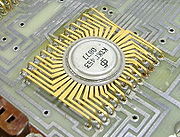
A chip carrier, also known as a chip container or chip package, is a container for a transistor or an integrated circuit. The carrier usually provides metal leads, or "pins", which are sturdy enough to electrically and mechanically connect the fragile chip to a circuit board. This connection may be...
, Chip carrier category).
Approaches
The earliest integrated circuits were packaged in ceramic flat packs, which continued to be used by the military for their reliability and small size for many years. Commercial circuit packaging quickly moved to the dual in-line packageDual in-line package
In microelectronics, a dual in-line package is an electronic device package with a rectangular housing and two parallel rows of electrical connecting pins. The package may be through-hole mounted to a printed circuit board or inserted in a socket.A DIP is usually referred to as a DIPn, where n is...
(DIP), first in ceramic and later in plastic. In the 1980s pin counts of VLSI circuits exceeded the practical limit for DIP packaging, leading to pin grid array
Pin grid array
A pin grid array, often abbreviated PGA, is a type of integrated circuit packaging. In a PGA, the package is square or roughly square, and the pins are arranged in a regular array on the underside of the package...
(PGA) and leadless chip carrier
Leadless chip carrier
A leadless chip carrier is a type of packaging for integrated circuits that has no "leads", but instead has rounded pins through the edges of the ceramic or molded plastic package....
(LCC) packages. Surface mount packaging appeared in the early 1980s and became popular in the late 1980s, using finer lead pitch with leads formed as either gull-wing or J-lead, as exemplified by small-outline integrated circuit
Small-Outline Integrated Circuit
A small-outline integrated circuit is a surface-mounted integrated circuit package which occupies an area about 30–50% less than an equivalent DIP, with a typical thickness that is 70% less. They are generally available in the same pinouts as their counterpart DIP ICs...
— a carrier which occupies an area about 30 – 50% less than an equivalent DIP
Dual in-line package
In microelectronics, a dual in-line package is an electronic device package with a rectangular housing and two parallel rows of electrical connecting pins. The package may be through-hole mounted to a printed circuit board or inserted in a socket.A DIP is usually referred to as a DIPn, where n is...
, with a typical thickness that is 70% less. This package has "gull wing" leads protruding from the two long sides and a lead spacing of 0.050 inches.
Small-outline integrated circuit
Small-Outline Integrated Circuit
A small-outline integrated circuit is a surface-mounted integrated circuit package which occupies an area about 30–50% less than an equivalent DIP, with a typical thickness that is 70% less. They are generally available in the same pinouts as their counterpart DIP ICs...
(SOIC) and Plastic leaded chip carrier
Plastic leaded chip carrier
A plastic leaded chip carrier is a chip carrier with a equiangular plastic housing. It is a reduced cost evolution of the ceramic leadless chip carrier ....
(PLCC) packages. In the late 1990s, plastic quad flat pack
PQFP
PQFP, or plastic quad flat pack, is a type of IC packaging. PQFP is a special case of QFP, as is the thinner TQFP package.PQFP packages can vary in thickness from 2.0 mm to 3.8 mm.-References:*...
(PQFP) and thin small-outline package
Thin small-outline package
Thin small-outline packages, or TSOPs are a type of surface mount IC package. They are notably very low-profile and have tight lead spacing ....
s (TSOP) became the most common for high pin count devices, though PGA packages are still often used for high-end microprocessor
Microprocessor
A microprocessor incorporates the functions of a computer's central processing unit on a single integrated circuit, or at most a few integrated circuits. It is a multipurpose, programmable device that accepts digital data as input, processes it according to instructions stored in its memory, and...
s. Intel and AMD are currently transitioning from PGA packages on high-end microprocessors to land grid array
Land grid array
The land grid array is a type of surface-mount packaging for integrated circuits that is notable for having the pins on the socket rather than the integrated circuit...
(LGA) packages.
Ball grid array
Ball grid array
A ball grid array is a type of surface-mount packaging used for integrated circuits.- Description :The BGA is descended from the pin grid array , which is a package with one face covered with pins in a grid pattern. These pins conduct electrical signals from the integrated circuit to the printed...
(BGA) packages have existed since the 1970s. Flip-chip Ball Grid Array packages, which allow for much higher pin count than other package types, were developed in the 1990s. In an FCBGA package the die is mounted upside-down (flipped) and connects to the package balls via a package substrate that is similar to a printed-circuit board rather than by wires. FCBGA packages allow an array of input-output signals (called Area-I/O) to be distributed over the entire die rather than being confined to the die periphery.
Traces out of the die, through the package, and into the printed circuit board
Printed circuit board
A printed circuit board, or PCB, is used to mechanically support and electrically connect electronic components using conductive pathways, tracks or signal traces etched from copper sheets laminated onto a non-conductive substrate. It is also referred to as printed wiring board or etched wiring...
have very different electrical properties, compared to on-chip signals. They require special design techniques and need much more electric power than signals confined to the chip itself.
When multiple dies are stacked in one package, it is called SiP, for System In Package
System in package
A system-in-a-package or system in package , also known as a Chip Stack MCM, is a number of integrated circuits enclosed in a single package or module. The SiP performs all or most of the functions of an electronic system, and are typically used inside a mobile phone, digital music player, etc...
, or three-dimensional integrated circuit
Three-dimensional integrated circuit
In electronics, a three-dimensional integrated circuit is a chip in which two or more layers of active electronic components are integrated both vertically and horizontally into a single circuit...
. When multiple dies are combined on a small substrate, often ceramic, it's called an MCM, or Multi-Chip Module
Multi-Chip Module
A multi-chip module is a specialized electronic package where multiple integrated circuits , semiconductor dies or other discrete components are packaged onto a unifying substrate, facilitating their use as a single component...
. The boundary between a big MCM and a small printed circuit board is sometimes fuzzy.
Operations
The following operations are performed at the stage of packaging.- Die attaching
- IC Bonding
- Wire bondingWire bondingWire bonding is the primary method of making interconnections between an integrated circuit and a printed circuit board during semiconductor device fabrication. Although less common, wire bonding can be used to connect an IC to other electronics or to connect from one PCB to another...
- Thermosonic BondingThermosonic BondingThermosonic bonding is widely used to permanently interconnect metallized silicon integrated circuits and other components into computers as well as into a myriad of other electronic equipment....
- Down bonding
- Flip chipFlip chipFlip chip, also known as Controlled Collapse Chip Connection or its acronym, C4, is a method for interconnecting semiconductor devices, such as IC chips and Microelectromechanical systems , to external circuitry with solder bumps that have been deposited onto the chip pads...
- Quilt packagingQuilt packagingQuilt Packaging is an electronic packaging technology under research that allows microchips made of dissimilar materials to be attached like squares in a quilt. Chips are connected in a way that minimizes both thermal stress and interchip delay times. The reflection coefficient s11 has been...
- Tab bonding
- Film attaching
- Spacer attaching
- Wire bonding
- IC encapsulation
- BakingBakingBaking is the technique of prolonged cooking of food by dry heat acting by convection, and not by radiation, normally in an oven, but also in hot ashes, or on hot stones. It is primarily used for the preparation of bread, cakes, pastries and pies, tarts, quiches, cookies and crackers. Such items...
- PlatingPlatingPlating is a surface covering in which a metal is deposited on a conductive surface. Plating has been done for hundreds of years, but it is also critical for modern technology...
- Lasermarking
- Trim and form
- Baking
- Wafer bondingWafer bondingWafer bonding is a packaging technology on wafer-level for the fabrication of microelectromechanical systems , nanoelectromechanical systems , microelectronics and optoelectronics, ensuring a mechanically stable and hermetically sealed encapsulation...
Unusual packaging
The vast majority of integrated circuits are packaged in opaque ceramic or plastic insulation.The only connection to the outside world is through metal pins (sometimes called "leads") through the insulation.
The rare exceptions include
proximity communication
"blob on PCB" (also known as Chip On Board or COB) that attaches the raw die directly to a PCB, bonds the die wires directly to the PCB traces, then covers the die and the die wires with a glob top of insulator;
and partially or totally transparent packaging for optical input and/or output of optoelectronic devices and EPROM
EPROM
An EPROM , or erasable programmable read only memory, is a type of memory chip that retains its data when its power supply is switched off. In other words, it is non-volatile. It is an array of floating-gate transistors individually programmed by an electronic device that supplies higher voltages...
.
See also
- Chip carrierChip carrierA chip carrier, also known as a chip container or chip package, is a container for a transistor or an integrated circuit. The carrier usually provides metal leads, or "pins", which are sturdy enough to electrically and mechanically connect the fragile chip to a circuit board. This connection may be...
(List of chip package types) - List of electronics package dimensions
- B-stagingB-stagingB-staging is a process that utilizes heat or UV light to remove the majority of solvent from an adhesive, thereby allowing construction to be “staged.” In between adhesive application, assembly and curing, the product can be held for a period of time, without sacrificing performance.Attempts to...
- Potting (electronics)Potting (electronics)In electronics, potting is a process of filling a complete electronic assembly with a solid or gelatinous compound for resistance to shock and vibration, and for exclusion of moisture and corrosive agents...
- Quilt packagingQuilt packagingQuilt Packaging is an electronic packaging technology under research that allows microchips made of dissimilar materials to be attached like squares in a quilt. Chips are connected in a way that minimizes both thermal stress and interchip delay times. The reflection coefficient s11 has been...
- Electronic packagingElectronic packagingElectronic packaging is a major discipline within the field of electronic engineering, and includes a wide variety of technologies. It refers to enclosures and protective features built into the product itself, and not to shipping containers...
External links
- wikia.com – Wikihowto on identifying chip packages
- ivf.se – The Nordic Electronics Packaging Guideline Investigation on the technical performance of different packaging and interconnection systems