
Hybrid silicon laser
Encyclopedia
A hybrid silicon laser is a semiconductor laser
fabricated from both silicon
and group III-V semiconductor materials. The hybrid silicon laser was developed to address the lack of a silicon laser to enable fabrication of low-cost, mass-producible silicon optical devices. The hybrid approach takes advantage of the light-emitting properties of III-V semiconductor materials combined with the process maturity of silicon to fabricate electrically driven lasers on a silicon wafer that can be integrated with other silicon photonic devices.
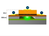
 A hybrid silicon laser is an optical source that is fabricated from both silicon
and group III-V semiconductor materials (e.g. Indium(III) phosphide
, Gallium(III) arsenide
). It comprises a silicon waveguide
fused to an active, light-emitting, III-V epitaxial semiconductor wafer. The III-V epitaxial wafer is designed with different layers such that the active layer can emit light when it is excited either by shining light, e.g. a laser
onto it; or by passing electricity through it. The emitted light from the active layer couples into the silicon waveguide due to their close proximity (<130 nm separation) where it can be guided to reflect off mirrors at the end of the silicon waveguide to form the laser cavity
.
(SOI) wafer. This SOI wafer and the un-patterned III-V wafer are then exposed to an oxygen plasma
before being pressed together at a low (for semiconductor manufacturing) temperature of 300C for 12hours. This process fuses the two wafers together. The III-V wafer is then etched into mesas to expose electrical layers in the epitaxial structure
. Metal contacts are fabricated on these contact layers allowing electrical current to flow to the active region.
suggests this light source could be used for optical communication
s when integrated with silicon photonics. Silicon manufacturing and fabrication is widely used in the electronic industry to mass-produce low-cost electronic devices. Silicon photonics uses these same electronic manufacturing technologies to make low cost integrated optical devices. One issue with using silicon for an optical device is that silicon is a poor light emitter and cannot be used to make an electrically pumped laser. This means that lasers have first to be fabricated on a separate III-V semiconductor wafer before being individually aligned to each silicon device, in a process that is both costly and time-consuming, limiting the total number of lasers that can be used on a silicon photonic circuit.
By using this wafer bonding technique many hybrid silicon lasers can be fabricated simultaneously on a silicon wafer, all aligned to the silicon photonic devices. Potential uses cited in the references below include fabricating many, possibly hundreds of hybrid silicon lasers on a die and using silicon photonics to combine them together to form high bandwidth optical links for personal computers, servers or back planes.
Laser
A laser is a device that emits light through a process of optical amplification based on the stimulated emission of photons. The term "laser" originated as an acronym for Light Amplification by Stimulated Emission of Radiation...
fabricated from both silicon
Silicon
Silicon is a chemical element with the symbol Si and atomic number 14. A tetravalent metalloid, it is less reactive than its chemical analog carbon, the nonmetal directly above it in the periodic table, but more reactive than germanium, the metalloid directly below it in the table...
and group III-V semiconductor materials. The hybrid silicon laser was developed to address the lack of a silicon laser to enable fabrication of low-cost, mass-producible silicon optical devices. The hybrid approach takes advantage of the light-emitting properties of III-V semiconductor materials combined with the process maturity of silicon to fabricate electrically driven lasers on a silicon wafer that can be integrated with other silicon photonic devices.
Physics
Silicon
Silicon is a chemical element with the symbol Si and atomic number 14. A tetravalent metalloid, it is less reactive than its chemical analog carbon, the nonmetal directly above it in the periodic table, but more reactive than germanium, the metalloid directly below it in the table...
and group III-V semiconductor materials (e.g. Indium(III) phosphide
Indium(III) phosphide
Indium phosphide is a binary semiconductor composed of indium and phosphorus. It has a face-centered cubic crystal structure, identical to that of GaAs and most of the III-V semiconductors....
, Gallium(III) arsenide
Gallium(III) arsenide
Gallium arsenide is a compound of the elements gallium and arsenic. It is a III/V semiconductor, and is used in the manufacture of devices such as microwave frequency integrated circuits, monolithic microwave integrated circuits, infrared light-emitting diodes, laser diodes, solar cells and...
). It comprises a silicon waveguide
Waveguide (optics)
An optical waveguide is a physical structure that guides electromagnetic waves in the optical spectrum. Common types of optical waveguides include optical fiber and rectangular waveguides....
fused to an active, light-emitting, III-V epitaxial semiconductor wafer. The III-V epitaxial wafer is designed with different layers such that the active layer can emit light when it is excited either by shining light, e.g. a laser
Laser
A laser is a device that emits light through a process of optical amplification based on the stimulated emission of photons. The term "laser" originated as an acronym for Light Amplification by Stimulated Emission of Radiation...
onto it; or by passing electricity through it. The emitted light from the active layer couples into the silicon waveguide due to their close proximity (<130 nm separation) where it can be guided to reflect off mirrors at the end of the silicon waveguide to form the laser cavity
Optical cavity
An optical cavity or optical resonator is an arrangement of mirrors that forms a standing wave cavity resonator for light waves. Optical cavities are a major component of lasers, surrounding the gain medium and providing feedback of the laser light. They are also used in optical parametric...
.
Fabrication
The hybrid silicon laser is fabricated by a technique called plasma assisted wafer bonding. Silicon waveguides are first fabricated on a silicon on insulatorSilicon on insulator
Silicon on insulator technology refers to the use of a layered silicon-insulator-silicon substrate in place of conventional silicon substrates in semiconductor manufacturing, especially microelectronics, to reduce parasitic device capacitance and thereby improving performance...
(SOI) wafer. This SOI wafer and the un-patterned III-V wafer are then exposed to an oxygen plasma
Plasma (physics)
In physics and chemistry, plasma is a state of matter similar to gas in which a certain portion of the particles are ionized. Heating a gas may ionize its molecules or atoms , thus turning it into a plasma, which contains charged particles: positive ions and negative electrons or ions...
before being pressed together at a low (for semiconductor manufacturing) temperature of 300C for 12hours. This process fuses the two wafers together. The III-V wafer is then etched into mesas to expose electrical layers in the epitaxial structure
Epitaxy
Epitaxy refers to the deposition of a crystalline overlayer on a crystalline substrate, where the overlayer is in registry with the substrate. In other words, there must be one or more preferred orientations of the overlayer with respect to the substrate for this to be termed epitaxial growth. The...
. Metal contacts are fabricated on these contact layers allowing electrical current to flow to the active region.
Uses
IntelIntel Corporation
Intel Corporation is an American multinational semiconductor chip maker corporation headquartered in Santa Clara, California, United States and the world's largest semiconductor chip maker, based on revenue. It is the inventor of the x86 series of microprocessors, the processors found in most...
suggests this light source could be used for optical communication
Optical communication
Optical communication is any form of telecommunication that uses light as the transmission medium.An optical communication system consists of a transmitter, which encodes a message into an optical signal, a channel, which carries the signal to its destination, and a receiver, which reproduces the...
s when integrated with silicon photonics. Silicon manufacturing and fabrication is widely used in the electronic industry to mass-produce low-cost electronic devices. Silicon photonics uses these same electronic manufacturing technologies to make low cost integrated optical devices. One issue with using silicon for an optical device is that silicon is a poor light emitter and cannot be used to make an electrically pumped laser. This means that lasers have first to be fabricated on a separate III-V semiconductor wafer before being individually aligned to each silicon device, in a process that is both costly and time-consuming, limiting the total number of lasers that can be used on a silicon photonic circuit.
By using this wafer bonding technique many hybrid silicon lasers can be fabricated simultaneously on a silicon wafer, all aligned to the silicon photonic devices. Potential uses cited in the references below include fabricating many, possibly hundreds of hybrid silicon lasers on a die and using silicon photonics to combine them together to form high bandwidth optical links for personal computers, servers or back planes.
History
- Pulsed optically pumped lasing first demonstrated by UCSBUniversity of California, Santa BarbaraThe University of California, Santa Barbara, commonly known as UCSB or UC Santa Barbara, is a public research university and one of the 10 general campuses of the University of California system. The main campus is located on a site in Goleta, California, from Santa Barbara and northwest of Los...
- Continuous wave optically pumped lasing demonstrated by IntelIntel CorporationIntel Corporation is an American multinational semiconductor chip maker corporation headquartered in Santa Clara, California, United States and the world's largest semiconductor chip maker, based on revenue. It is the inventor of the x86 series of microprocessors, the processors found in most...
and UCSB - Continuous wave electrically driven lasing demonstrated by UCSB and Intel