

Gallium(III) arsenide
Encyclopedia
Gallium arsenide is a compound
of the elements gallium
and arsenic
. It is a III
/V
semiconductor
, and is used in the manufacture of devices such as microwave
frequency integrated circuit
s, monolithic microwave integrated circuit
s, infrared
light-emitting diode
s, laser diode
s, solar cells and optical windows.
. Gallium arsenide can be prepared by direct reaction from the elements which is used in a number of industrial processes:
Alternative methods for producing films of GaAs include:
or
Wet etching of GaAs industrially uses an oxidizing agent, for example hydrogen peroxide
or bromine
water, and the same strategy has been described in a patent relating to processing scrap components containing GaAs where the Ga3+ is complexed with a hydroxamic acid
("HA"), for example::
Oxidation of GaAs occurs in air and degrades performance of the semiconductor. The surface can be passivated by depositing a cubic gallium(II) sulfide
layer using a tert-butyl gallium sulfide compound such as (tBuGaS)7.
. It has a higher saturated electron velocity
and higher electron mobility
, allowing transistors made from it to function at frequencies in excess of 250 GHz. Unlike silicon junctions, GaAs devices are relatively insensitive to heat owing to their wider bandgap. Also, GaAs devices tend to have less noise than silicon devices especially at high frequencies which is a result of higher carrier mobilities and lower resistive device parasitics. These properties recommend GaAs circuitry in mobile phone
s, satellite
communications, microwave point-to-point links and higher frequency radar
systems. It is used in the manufacture of Gunn diode
s for generation of microwaves.
Another advantage of GaAs is that it has a direct band gap, which means that it can be used to emit light efficiently. Silicon has an indirect bandgap and so is very poor at emitting light. Nonetheless, recent advances may make silicon LED
s and laser
s possible.
As a wide direct band gap material and resulting resistance to radiation damage, GaAs is an excellent material for space electronics and optical windows in high power applications.
Because of its wide bandgap, pure GaAs is highly resistive. Combined with the high dielectric constant, this property makes GaAs a very good electrical substrate and unlike Si provides natural isolation between devices and circuits. This has made it an ideal material for microwave and millimeter wave integrated circuits, MMICs, where active and essential passive components can readily be produced on a single slice of GaAs.
One of the first GaAs microprocessor
s was developed in the early 1980s by the RCA
corporation and was considered for the Star Wars program
of the United States Department of Defense
. Those processors were several times faster and several orders of magnitude more radiation hard
than silicon counterparts, but they were rather expensive. Other GaAs processors were implemented by the supercomputer
vendors Cray Computer Corporation, Convex
, and Alliant
in an attempt to stay ahead of the ever-improving CMOS
microprocessor. Cray eventually built one GaAs-based machine in the early 1990s, the Cray-3
, but the effort was not adequately capitalized, and the company filed for bankruptcy in 1995.
Complex layered structures of gallium arsenide in combination with aluminium arsenide
(AlAs) or the alloy AlxGa1-xAs
can be grown using molecular beam epitaxy
(MBE) or using metalorganic vapor phase epitaxy (MOVPE). Because GaAs and AlAs have almost the same lattice constant
, the layers have very little induced strain
, which allows them to be grown almost arbitrarily thick. This allows for extremely high performance high electron mobility, HEMT
transistors and other quantum well
devices.
minerals. The economy of scale available to the silicon industry has also reduced the adoption of GaAs.
In addition, a Si crystal has an extremely stable structure mechanically and it can be grown to very large diameter boules and can be processed with very high yields. It is also a decent thermal conductor thus enable very dense packing of transistors, all very desirable for design and manufacturing of very large IC
s. Such good mechanical characteristics also makes it a suitable material for the rapidly developing field of nanoelectronics
.
The second major advantage of Si is the existence of a native oxide (silicon dioxide
), which is used as an insulator
in electronic devices. Silicon dioxide can easily be incorporated onto silicon circuits, and such layers are adherent to the underlying Si. GaAs does not have a native oxide and does not easily support a stable adherent insulating layer.
The third, and perhaps most important, advantage of silicon is that it possesses a much higher hole
mobility. This high mobility allows the fabrication of higher-speed P-channel field effect transistors, which are required for CMOS logic. Because they lack a fast CMOS structure, GaAs logic circuits have much higher power consumption, which has made them unable to compete with silicon logic circuits.
Silicon has relatively low absorptivity
for the sunlight meaning about 100 micrometers of Si is needed to absorb most sunlight. Such a layer is relatively robust and easy to handle. In contrast, the absorptivity of GaAs is so high that a corresponding layer would be only a few micrometers thick and mechanically unstable.
Silicon is a pure element, avoiding the problems of stoichiometric imbalance and thermal unmixing of GaAs.
Silicon has a nearly perfect lattice, impurity density is very low and allows to build very small structures (currently down to 25 nm). GaAs in contrast has a very high impurity density, which makes it difficult to build ICs with small structures, so the 500 nm process is a common process for GaAs.
s. Gallium arsenide (GaAs) is also known as single-crystalline thin film
and are high cost high efficiency solar cell
s.
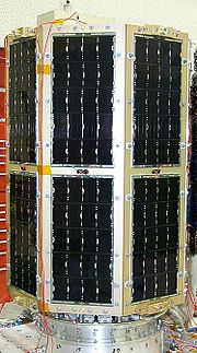
In 1970, the first GaAs heterostructure solar cells were created by the team led by Zhores Alferov in the USSR. In the early 1980s, the efficiency of the best GaAs solar cells surpassed that of silicon solar cells, and in the 1990s GaAs solar cells took over from silicon as the cell type most commonly used for Photovoltaic arrays for satellite applications. Later, dual- and triple-junction solar cells
based on GaAs with germanium
and indium gallium phosphide
layers were developed as the basis of a triple junction solar cell which held a record efficiency of over 32% and can operate also with light as concentrated as 2,000 suns. This kind of solar cell powers the rovers
Spirit
and Opportunity
, which are exploring Mars
' surface. Also many solar car
s utilize GaAs in solar arrays.
Complex designs of AlxGa1-xAs-GaAs devices can be sensitive to infrared radiation (QWIP).
GaAs diodes can be used for the detection of X-rays.
Single crystal
s of gallium arsenide can be manufactured by the Bridgeman technique
, as the Czochralski process
is difficult for this material due to its mechanical properties. However, an encapsulated Czochralski method is used to produce ultra-high purity GaAs for semi-insulators.
GaAs is often used as a substrate material for the epitaxial growth of other III-V semiconductors including: InGaAs and GaInNAs.
and arsine
) and industrial hygiene monitoring studies of metalorganic precursors have been reported. California lists gallium arsenide as a carcinogen.
Chemical compound
A chemical compound is a pure chemical substance consisting of two or more different chemical elements that can be separated into simpler substances by chemical reactions. Chemical compounds have a unique and defined chemical structure; they consist of a fixed ratio of atoms that are held together...
of the elements gallium
Gallium
Gallium is a chemical element that has the symbol Ga and atomic number 31. Elemental gallium does not occur in nature, but as the gallium salt in trace amounts in bauxite and zinc ores. A soft silvery metallic poor metal, elemental gallium is a brittle solid at low temperatures. As it liquefies...
and arsenic
Arsenic
Arsenic is a chemical element with the symbol As, atomic number 33 and relative atomic mass 74.92. Arsenic occurs in many minerals, usually in conjunction with sulfur and metals, and also as a pure elemental crystal. It was first documented by Albertus Magnus in 1250.Arsenic is a metalloid...
. It is a III
Boron group
The boron group is the series of elements in group 13 of the periodic table, comprising boron , aluminium , gallium , indium , thallium , and ununtrium . The elements in the boron group are characterized by having three electrons in their outer energy levels...
/V
Nitrogen group
The nitrogen group is a periodic table group consisting of nitrogen , phosphorus , arsenic , antimony , bismuth and ununpentium ....
semiconductor
Semiconductor
A semiconductor is a material with electrical conductivity due to electron flow intermediate in magnitude between that of a conductor and an insulator. This means a conductivity roughly in the range of 103 to 10−8 siemens per centimeter...
, and is used in the manufacture of devices such as microwave
Microwave
Microwaves, a subset of radio waves, have wavelengths ranging from as long as one meter to as short as one millimeter, or equivalently, with frequencies between 300 MHz and 300 GHz. This broad definition includes both UHF and EHF , and various sources use different boundaries...
frequency integrated circuit
Integrated circuit
An integrated circuit or monolithic integrated circuit is an electronic circuit manufactured by the patterned diffusion of trace elements into the surface of a thin substrate of semiconductor material...
s, monolithic microwave integrated circuit
Monolithic Microwave Integrated Circuit
A Monolithic Microwave Integrated Circuit, or MMIC , is a type of integrated circuit device that operates at microwave frequencies . These devices typically perform functions such as microwave mixing, power amplification, low noise amplification, and high frequency switching...
s, infrared
Infrared
Infrared light is electromagnetic radiation with a wavelength longer than that of visible light, measured from the nominal edge of visible red light at 0.74 micrometres , and extending conventionally to 300 µm...
light-emitting diode
Light-emitting diode
A light-emitting diode is a semiconductor light source. LEDs are used as indicator lamps in many devices and are increasingly used for other lighting...
s, laser diode
Laser diode
The laser diode is a laser where the active medium is a semiconductor similar to that found in a light-emitting diode. The most common type of laser diode is formed from a p-n junction and powered by injected electric current...
s, solar cells and optical windows.
Preparation and chemistry
In the compound, gallium has a +3 oxidation stateOxidation state
In chemistry, the oxidation state is an indicator of the degree of oxidation of an atom in a chemical compound. The formal oxidation state is the hypothetical charge that an atom would have if all bonds to atoms of different elements were 100% ionic. Oxidation states are typically represented by...
. Gallium arsenide can be prepared by direct reaction from the elements which is used in a number of industrial processes:
- Crystal growth using a horizontal zone furnace in the Bridgman-Stockbarger technique, in which gallium and arsenic vapors react and free molecules deposit on a seed crystal at the cooler end of the furnace.
- Liquid encapsulated CzochralskiCzochralski processThe Czochralski process is a method of crystal growth used to obtain single crystals of semiconductors , metals , salts, and synthetic gemstones...
(LEC) growth is used for producing high purity single crystals that exhibit semi-insulating characteristics.
Alternative methods for producing films of GaAs include:
- VPEChemical vapor depositionChemical vapor deposition is a chemical process used to produce high-purity, high-performance solid materials. The process is often used in the semiconductor industry to produce thin films. In a typical CVD process, the wafer is exposed to one or more volatile precursors, which react and/or...
reaction of gaseous gallium metal and arsenic trichlorideArsenic trichlorideArsenic trichloride is an inorganic compound with the formula AsCl3, also known as arsenous chloride or butter of arsenic. This poisonous oil is colourless, although impure samples may appear yellow. It is an intermediate in the manufacture of organoarsenic compounds.-Structure:AsCl3 is a...
:
- 2 Ga + 2 AsCl3 → 2 GaAs + 3 Cl2
- MOCVD reaction of trimethylgalliumTrimethylgalliumTrimethylgallium, Ga3, often abbreviated to TMG or TMGa, is the preferred metalorganic source of gallium for metalorganic vapour phase epitaxy of gallium-containing compound semiconductors, such as GaAs, GaN, GaP, GaSb, InGaAs, InGaN, AlGaInP, InGaP and AlInGaNP.-Properties:TMG is a clear,...
and arsineArsineArsine is the chemical compound with the formula AsH3. This flammable, pyrophoric, and highly toxic gas is one of the simplest compounds of arsenic...
:
- MOCVD reaction of trimethylgallium
- Ga(CH3)3 + AsH3 → GaAs + 3 CH4
- Molecular beam epitaxyMolecular beam epitaxyMolecular beam epitaxy is one of several methods of depositing single crystals. It was invented in the late 1960s at Bell Telephone Laboratories by J. R. Arthur and Alfred Y. Cho.-Method:...
(MBE) of galliumGalliumGallium is a chemical element that has the symbol Ga and atomic number 31. Elemental gallium does not occur in nature, but as the gallium salt in trace amounts in bauxite and zinc ores. A soft silvery metallic poor metal, elemental gallium is a brittle solid at low temperatures. As it liquefies...
and arsenicArsenicArsenic is a chemical element with the symbol As, atomic number 33 and relative atomic mass 74.92. Arsenic occurs in many minerals, usually in conjunction with sulfur and metals, and also as a pure elemental crystal. It was first documented by Albertus Magnus in 1250.Arsenic is a metalloid...
:
- Molecular beam epitaxy
- 4 Ga + As4 → 4 GaAs
or
- 2 Ga + As2 → 2 GaAs
Wet etching of GaAs industrially uses an oxidizing agent, for example hydrogen peroxide
Hydrogen peroxide
Hydrogen peroxide is the simplest peroxide and an oxidizer. Hydrogen peroxide is a clear liquid, slightly more viscous than water. In dilute solution, it appears colorless. With its oxidizing properties, hydrogen peroxide is often used as a bleach or cleaning agent...
or bromine
Bromine
Bromine ") is a chemical element with the symbol Br, an atomic number of 35, and an atomic mass of 79.904. It is in the halogen element group. The element was isolated independently by two chemists, Carl Jacob Löwig and Antoine Jerome Balard, in 1825–1826...
water, and the same strategy has been described in a patent relating to processing scrap components containing GaAs where the Ga3+ is complexed with a hydroxamic acid
Hydroxamic acid
A hydroxamic acid is a class of chemical compounds sharing the same functional group in which an hydroxylamine is inserted into a carboxylic acid. Its general structure is R-CO-NH-OH, with an R as an organic residue, a CO as a carbonyl group, and a hydroxylamine as NH2-OH. They are used as metal...
("HA"), for example::
- GaAs + H2O2 + "HA" → "GaA" complex + H3AsO4 + 4 H2O
Oxidation of GaAs occurs in air and degrades performance of the semiconductor. The surface can be passivated by depositing a cubic gallium(II) sulfide
Gallium(II) sulfide
Gallium sulfide, GaS, is a chemical compound of gallium and sulfur. The normal form of gallium sulfide as made from the elements has a hexagonal layer structure containing Ga24+ units which have a Ga-Ga distance of 248pm. This layer structure is similar to GaTe, GaSe and InSe...
layer using a tert-butyl gallium sulfide compound such as (tBuGaS)7.
GaAs advantages
GaAs has some electronic properties which are superior to those of siliconSilicon
Silicon is a chemical element with the symbol Si and atomic number 14. A tetravalent metalloid, it is less reactive than its chemical analog carbon, the nonmetal directly above it in the periodic table, but more reactive than germanium, the metalloid directly below it in the table...
. It has a higher saturated electron velocity
Saturation velocity
Saturation velocity is the maximum velocity a charge carrier in a semiconductor, generally an electron, attains in the presence of very high electric fields. Charge carriers normally move at an average drift speed proportional to the electric field strength they experience temporally. The...
and higher electron mobility
Electron mobility
In solid-state physics, the electron mobility characterizes how quickly an electron can move through a metal or semiconductor, when pulled by an electric field. In semiconductors, there is an analogous quantity for holes, called hole mobility...
, allowing transistors made from it to function at frequencies in excess of 250 GHz. Unlike silicon junctions, GaAs devices are relatively insensitive to heat owing to their wider bandgap. Also, GaAs devices tend to have less noise than silicon devices especially at high frequencies which is a result of higher carrier mobilities and lower resistive device parasitics. These properties recommend GaAs circuitry in mobile phone
Mobile phone
A mobile phone is a device which can make and receive telephone calls over a radio link whilst moving around a wide geographic area. It does so by connecting to a cellular network provided by a mobile network operator...
s, satellite
Communications satellite
A communications satellite is an artificial satellite stationed in space for the purpose of telecommunications...
communications, microwave point-to-point links and higher frequency radar
Radar
Radar is an object-detection system which uses radio waves to determine the range, altitude, direction, or speed of objects. It can be used to detect aircraft, ships, spacecraft, guided missiles, motor vehicles, weather formations, and terrain. The radar dish or antenna transmits pulses of radio...
systems. It is used in the manufacture of Gunn diode
Gunn diode
A Gunn diode, also known as a transferred electron device , is a form of diode used in high-frequency electronics. It is somewhat unusual in that it consists only of N-doped semiconductor material, whereas most diodes consist of both P and N-doped regions...
s for generation of microwaves.
Another advantage of GaAs is that it has a direct band gap, which means that it can be used to emit light efficiently. Silicon has an indirect bandgap and so is very poor at emitting light. Nonetheless, recent advances may make silicon LED
LEd
LEd is a TeX/LaTeX editing software working under Microsoft Windows. It is a freeware product....
s and laser
Laser
A laser is a device that emits light through a process of optical amplification based on the stimulated emission of photons. The term "laser" originated as an acronym for Light Amplification by Stimulated Emission of Radiation...
s possible.
As a wide direct band gap material and resulting resistance to radiation damage, GaAs is an excellent material for space electronics and optical windows in high power applications.
Because of its wide bandgap, pure GaAs is highly resistive. Combined with the high dielectric constant, this property makes GaAs a very good electrical substrate and unlike Si provides natural isolation between devices and circuits. This has made it an ideal material for microwave and millimeter wave integrated circuits, MMICs, where active and essential passive components can readily be produced on a single slice of GaAs.
One of the first GaAs microprocessor
Microprocessor
A microprocessor incorporates the functions of a computer's central processing unit on a single integrated circuit, or at most a few integrated circuits. It is a multipurpose, programmable device that accepts digital data as input, processes it according to instructions stored in its memory, and...
s was developed in the early 1980s by the RCA
RCA
RCA Corporation, founded as the Radio Corporation of America, was an American electronics company in existence from 1919 to 1986. The RCA trademark is currently owned by the French conglomerate Technicolor SA through RCA Trademark Management S.A., a company owned by Technicolor...
corporation and was considered for the Star Wars program
Strategic Defense Initiative
The Strategic Defense Initiative was proposed by U.S. President Ronald Reagan on March 23, 1983 to use ground and space-based systems to protect the United States from attack by strategic nuclear ballistic missiles. The initiative focused on strategic defense rather than the prior strategic...
of the United States Department of Defense
United States Department of Defense
The United States Department of Defense is the U.S...
. Those processors were several times faster and several orders of magnitude more radiation hard
Radiation hardening
Radiation hardening is a method of designing and testing electronic components and systems to make them resistant to damage or malfunctions caused by ionizing radiation , such as would be encountered in outer space, high-altitude flight, around nuclear reactors, particle accelerators, or during...
than silicon counterparts, but they were rather expensive. Other GaAs processors were implemented by the supercomputer
Supercomputer
A supercomputer is a computer at the frontline of current processing capacity, particularly speed of calculation.Supercomputers are used for highly calculation-intensive tasks such as problems including quantum physics, weather forecasting, climate research, molecular modeling A supercomputer is a...
vendors Cray Computer Corporation, Convex
Convex Computer
Convex Computer Corporation was a company that developed, manufactured and marketed vector minisupercomputers and supercomputers for small-to-medium-sized businesses. Their later Exemplar series of parallel computing machines were based on the Hewlett-Packard PA-RISC microprocessors, and in 1995,...
, and Alliant
Alliant Computer Systems
Alliant Computer Systems was a computer company that designed and manufactured parallel computing systems. Together with Pyramid Technology and Sequent Computer Systems, Alliant's machines pioneered the symmetric multiprocessing market...
in an attempt to stay ahead of the ever-improving CMOS
CMOS
Complementary metal–oxide–semiconductor is a technology for constructing integrated circuits. CMOS technology is used in microprocessors, microcontrollers, static RAM, and other digital logic circuits...
microprocessor. Cray eventually built one GaAs-based machine in the early 1990s, the Cray-3
Cray-3
The Cray-3 was a vector supercomputer intended to be Cray Research's successor to the Cray-2. The system was to be the first major application of gallium arsenide semiconductors in computing. The project was not considered a success, and the parent company in Minneapolis decided to end work on the...
, but the effort was not adequately capitalized, and the company filed for bankruptcy in 1995.
Complex layered structures of gallium arsenide in combination with aluminium arsenide
Aluminium arsenide
Aluminium arsenide or aluminum arsenide is a semiconductor material with almost the same lattice constant as gallium arsenide and aluminium gallium arsenide and wider band gap than gallium arsenide.-Properties:...
(AlAs) or the alloy AlxGa1-xAs
Aluminium gallium arsenide
Aluminium gallium arsenide is a semiconductor material with very nearly the same lattice constant as GaAs, but a larger bandgap. The x in the formula above is a number between 0 and 1 - this indicates an arbitrary alloy between GaAs and AlAs.The bandgap varies between 1.42 eV and 2.16 eV...
can be grown using molecular beam epitaxy
Molecular beam epitaxy
Molecular beam epitaxy is one of several methods of depositing single crystals. It was invented in the late 1960s at Bell Telephone Laboratories by J. R. Arthur and Alfred Y. Cho.-Method:...
(MBE) or using metalorganic vapor phase epitaxy (MOVPE). Because GaAs and AlAs have almost the same lattice constant
Lattice constant
The lattice constant [or lattice parameter] refers to the constant distance between unit cells in a crystal lattice. Lattices in three dimensions generally have three lattice constants, referred to as a, b, and c. However, in the special case of cubic crystal structures, all of the constants are...
, the layers have very little induced strain
Strain (chemistry)
In chemistry, a molecule experiences strain when its chemical structure undergoes some stress which raises its internal energy in comparison to a strain-free reference compound. The internal energy of a molecule consists of all the energy stored within it. A strained molecule has an additional...
, which allows them to be grown almost arbitrarily thick. This allows for extremely high performance high electron mobility, HEMT
HEMT
High electron mobility transistor , also known as heterostructure FET or modulation-doped FET , is a field effect transistor incorporating a junction between two materials with different band gaps as the channel instead of a doped region, as is generally the case for MOSFET...
transistors and other quantum well
Quantum well
A quantum well is a potential well with only discrete energy values.One technology to create quantization is to confine particles, which were originally free to move in three dimensions, to two dimensions, forcing them to occupy a planar region...
devices.
Silicon advantages
Silicon has three major advantages over GaAs for integrated circuit manufacture. First, silicon is abundant and cheap to process. Si is highly abundant in the Earth's crust, in the form of silicateSilicate
A silicate is a compound containing a silicon bearing anion. The great majority of silicates are oxides, but hexafluorosilicate and other anions are also included. This article focuses mainly on the Si-O anions. Silicates comprise the majority of the earth's crust, as well as the other...
minerals. The economy of scale available to the silicon industry has also reduced the adoption of GaAs.
In addition, a Si crystal has an extremely stable structure mechanically and it can be grown to very large diameter boules and can be processed with very high yields. It is also a decent thermal conductor thus enable very dense packing of transistors, all very desirable for design and manufacturing of very large IC
Ic
IC, ic, or i.c. may stand for:In computing and technology:* .ic.gov, a second-level domain name administered by the US Government for members of the intelligence community* Integrated circuit* Initial condition...
s. Such good mechanical characteristics also makes it a suitable material for the rapidly developing field of nanoelectronics
Nanoelectronics
Nanoelectronics refer to the use of nanotechnology on electronic components, especially transistors. Although the term nanotechnology is generally defined as utilizing technology less than 100 nm in size, nanoelectronics often refer to transistor devices that are so small that inter-atomic...
.
The second major advantage of Si is the existence of a native oxide (silicon dioxide
Silicon dioxide
The chemical compound silicon dioxide, also known as silica , is an oxide of silicon with the chemical formula '. It has been known for its hardness since antiquity...
), which is used as an insulator
Electrical insulation
thumb|250px|[[Coaxial Cable]] with dielectric insulator supporting a central coreThis article refers to electrical insulation. For insulation of heat, see Thermal insulation...
in electronic devices. Silicon dioxide can easily be incorporated onto silicon circuits, and such layers are adherent to the underlying Si. GaAs does not have a native oxide and does not easily support a stable adherent insulating layer.
The third, and perhaps most important, advantage of silicon is that it possesses a much higher hole
Electron hole
An electron hole is the conceptual and mathematical opposite of an electron, useful in the study of physics, chemistry, and electrical engineering. The concept describes the lack of an electron at a position where one could exist in an atom or atomic lattice...
mobility. This high mobility allows the fabrication of higher-speed P-channel field effect transistors, which are required for CMOS logic. Because they lack a fast CMOS structure, GaAs logic circuits have much higher power consumption, which has made them unable to compete with silicon logic circuits.
Silicon has relatively low absorptivity
Absorptivity
The term absorptivity has two meanings:*In chemistry, it usually refers to Molar absorptivity : the constant \epsilon used in the Beer-Lambert law, A=\epsilon c l, where A is the absorbance, c is the concentration of the solution, and l is the path length....
for the sunlight meaning about 100 micrometers of Si is needed to absorb most sunlight. Such a layer is relatively robust and easy to handle. In contrast, the absorptivity of GaAs is so high that a corresponding layer would be only a few micrometers thick and mechanically unstable.
Silicon is a pure element, avoiding the problems of stoichiometric imbalance and thermal unmixing of GaAs.
Silicon has a nearly perfect lattice, impurity density is very low and allows to build very small structures (currently down to 25 nm). GaAs in contrast has a very high impurity density, which makes it difficult to build ICs with small structures, so the 500 nm process is a common process for GaAs.
Solar cells and detectors
Another important application of GaAs is for high efficiency solar cellSolar cell
A solar cell is a solid state electrical device that converts the energy of light directly into electricity by the photovoltaic effect....
s. Gallium arsenide (GaAs) is also known as single-crystalline thin film
Thin film
A thin film is a layer of material ranging from fractions of a nanometer to several micrometers in thickness. Electronic semiconductor devices and optical coatings are the main applications benefiting from thin film construction....
and are high cost high efficiency solar cell
Solar cell
A solar cell is a solid state electrical device that converts the energy of light directly into electricity by the photovoltaic effect....
s.
In 1970, the first GaAs heterostructure solar cells were created by the team led by Zhores Alferov in the USSR. In the early 1980s, the efficiency of the best GaAs solar cells surpassed that of silicon solar cells, and in the 1990s GaAs solar cells took over from silicon as the cell type most commonly used for Photovoltaic arrays for satellite applications. Later, dual- and triple-junction solar cells
Multijunction photovoltaic cell
Multi-junction solar cells or tandem cells are solar cells containing several p-n junctions. Each junction is tuned to a different wavelength of light, reducing one of the largest inherent sources of losses, and thereby increasing efficiency...
based on GaAs with germanium
Germanium
Germanium is a chemical element with the symbol Ge and atomic number 32. It is a lustrous, hard, grayish-white metalloid in the carbon group, chemically similar to its group neighbors tin and silicon. The isolated element is a semiconductor, with an appearance most similar to elemental silicon....
and indium gallium phosphide
Indium gallium phosphide
Indium gallium phosphide , also called gallium indium phosphide , is a semiconductor composed of indium, gallium and phosphorus...
layers were developed as the basis of a triple junction solar cell which held a record efficiency of over 32% and can operate also with light as concentrated as 2,000 suns. This kind of solar cell powers the rovers
Rover (space exploration)
A rover is a space exploration vehicle designed to move across the surface of a planet or other astronomical body. Some rovers have been designed to transport members of a human spaceflight crew; others have been partially or fully autonomous robots...
Spirit
Spirit rover
Spirit, MER-A , is a robotic rover on Mars, active from 2004 to 2010. It was one of two rovers of NASA's ongoing Mars Exploration Rover Mission. It landed successfully on Mars at 04:35 Ground UTC on January 4, 2004, three weeks before its twin, Opportunity , landed on the other side of the planet...
and Opportunity
Opportunity rover
Opportunity, MER-B , is a robotic rover on the planet Mars, active since 2004. It is the remaining rover in NASA's ongoing Mars Exploration Rover Mission...
, which are exploring Mars
Mars
Mars is the fourth planet from the Sun in the Solar System. The planet is named after the Roman god of war, Mars. It is often described as the "Red Planet", as the iron oxide prevalent on its surface gives it a reddish appearance...
' surface. Also many solar car
Solar car racing
Solar car racing refers to competitive races of electric vehicles which are powered by solar energy obtained from solar panels on the surface of the car . The first solar car race was the Tour de Sol in 1985 which led to several similar races in Europe, USA and Australia...
s utilize GaAs in solar arrays.
Complex designs of AlxGa1-xAs-GaAs devices can be sensitive to infrared radiation (QWIP).
GaAs diodes can be used for the detection of X-rays.
Light emission devices
GaAs has been used to produce (near-infrared) laser diodes since 1962.Single crystal
Single crystal
A single crystal or monocrystalline solid is a material in which the crystal lattice of the entire sample is continuous and unbroken to the edges of the sample, with no grain boundaries...
s of gallium arsenide can be manufactured by the Bridgeman technique
Bridgeman technique
The Bridgman–Stockbarger technique is named after Harvard physicist Percy Williams Bridgman and MIT physicist Donald C. Stockbarger...
, as the Czochralski process
Czochralski process
The Czochralski process is a method of crystal growth used to obtain single crystals of semiconductors , metals , salts, and synthetic gemstones...
is difficult for this material due to its mechanical properties. However, an encapsulated Czochralski method is used to produce ultra-high purity GaAs for semi-insulators.
GaAs is often used as a substrate material for the epitaxial growth of other III-V semiconductors including: InGaAs and GaInNAs.
Safety
The toxicological properties of gallium arsenide have not been thoroughly investigated. On one hand, due to its arsenic content, it is considered highly toxic and carcinogenic. On the other hand, the crystal is stable enough that ingested pieces may be passed with negligible absorption by the body. When ground into very fine particles, such as in wafer-polishing processes, the high surface area enables more reaction with water releasing some arsine and/or dissolved arsenic. The environment, health and safety aspects of gallium arsenide sources (such as trimethylgalliumTrimethylgallium
Trimethylgallium, Ga3, often abbreviated to TMG or TMGa, is the preferred metalorganic source of gallium for metalorganic vapour phase epitaxy of gallium-containing compound semiconductors, such as GaAs, GaN, GaP, GaSb, InGaAs, InGaN, AlGaInP, InGaP and AlInGaNP.-Properties:TMG is a clear,...
and arsine
Arsine
Arsine is the chemical compound with the formula AsH3. This flammable, pyrophoric, and highly toxic gas is one of the simplest compounds of arsenic...
) and industrial hygiene monitoring studies of metalorganic precursors have been reported. California lists gallium arsenide as a carcinogen.
See also
- Aluminium arsenideAluminium arsenideAluminium arsenide or aluminum arsenide is a semiconductor material with almost the same lattice constant as gallium arsenide and aluminium gallium arsenide and wider band gap than gallium arsenide.-Properties:...
- Aluminium gallium arsenideAluminium gallium arsenideAluminium gallium arsenide is a semiconductor material with very nearly the same lattice constant as GaAs, but a larger bandgap. The x in the formula above is a number between 0 and 1 - this indicates an arbitrary alloy between GaAs and AlAs.The bandgap varies between 1.42 eV and 2.16 eV...
- ArsineArsineArsine is the chemical compound with the formula AsH3. This flammable, pyrophoric, and highly toxic gas is one of the simplest compounds of arsenic...
- Cadmium tellurideCadmium tellurideCadmium telluride is a crystalline compound formed from cadmium and tellurium. It is used as an infrared optical window and a solar cell material. It is usually sandwiched with cadmium sulfide to form a p-n junction photovoltaic solar cell...
- Gallium antimonide
- Gallium arsenide phosphideGallium arsenide phosphideGallium arsenide phosphide is a semiconductor material, an alloy of gallium arsenide and gallium phosphide. It exists in various composition ratios indicated in its formula by the fraction x....
- Gallium manganese arsenide
- Gallium phosphide
- Gallium nitride
- Heterostructure emitter bipolar transistor
- Indium arsenide
- Indium gallium arsenideIndium gallium arsenideIndium gallium arsenide is a semiconductor composed of indium, gallium and arsenic. It is used in high-power and high-frequency electronics because of its superior electron velocity with respect to the more common semiconductors silicon and gallium arsenide. InGaAs bandgap also makes it the...
- Indium phosphide
- Light-emitting diodeLight-emitting diodeA light-emitting diode is a semiconductor light source. LEDs are used as indicator lamps in many devices and are increasingly used for other lighting...
- MOVPE
- Multijunction
- PhotomixingPhotomixingPhotomixing is the generation of continuous wave terahertz radiation from two lasers. The beams are mixed together and focussed onto a photomixer device which generates the terahertz radiation....
- TrimethylgalliumTrimethylgalliumTrimethylgallium, Ga3, often abbreviated to TMG or TMGa, is the preferred metalorganic source of gallium for metalorganic vapour phase epitaxy of gallium-containing compound semiconductors, such as GaAs, GaN, GaP, GaSb, InGaAs, InGaN, AlGaInP, InGaP and AlInGaNP.-Properties:TMG is a clear,...