

Electron beam induced current
Encyclopedia
Scanning electron microscope
A scanning electron microscope is a type of electron microscope that images a sample by scanning it with a high-energy beam of electrons in a raster scan pattern...
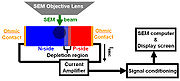
(SEM) or scanning transmission electron microscope (STEM). It is used to identify buried junctions or defects in semiconductors, or to examine minority carrier properties. EBIC is similar to cathodoluminescence
Cathodoluminescence
Cathodoluminescence is an optical and electrical phenomenon whereby a beam of electrons is generated by an electron gun and then impacts on a luminescent material such as a phosphor, causing the material to emit visible light. The most common example is the screen of a television...
in that it depends on the creation of electron–hole pairs in the semiconductor sample by the microscope's electron beam. This technique is used in semiconductor failure analysis
Failure analysis
Failure analysis is the process of collecting and analyzing data to determine the cause of a failure. It is an important discipline in many branches of manufacturing industry, such as the electronics industry, where it is a vital tool used in the development of new products and for the improvement...
and solid-state physics
Solid-state physics
Solid-state physics is the study of rigid matter, or solids, through methods such as quantum mechanics, crystallography, electromagnetism, and metallurgy. It is the largest branch of condensed matter physics. Solid-state physics studies how the large-scale properties of solid materials result from...
.
Physics of the Technique
If the semiconductor sample contains an internal electric fieldElectric field
In physics, an electric field surrounds electrically charged particles and time-varying magnetic fields. The electric field depicts the force exerted on other electrically charged objects by the electrically charged particle the field is surrounding...
, as will be present in the depletion region
Depletion region
In semiconductor physics, the depletion region, also called depletion layer, depletion zone, junction region or the space charge region, is an insulating region within a conductive, doped semiconductor material where the mobile charge carriers have diffused away, or have been forced away by an...
at a p-n junction
P-n junction
A p–n junction is formed at the boundary between a P-type and N-type semiconductor created in a single crystal of semiconductor by doping, for example by ion implantation, diffusion of dopants, or by epitaxy .If two separate pieces of material were used, this would...
or schottky junction
Schottky diode
The Schottky diode is a semiconductor diode with a low forward voltage drop and a very fast switching action...
, the electron–hole pairs will be separated by drift due to the electric field. If the p- and n-sides (or semiconductor and schottky contact, in the case of a schottky device) are connected through a picoammeter, a current will flow.
EBIC is best understood by analogy: in a solar cell
Solar cell
A solar cell is a solid state electrical device that converts the energy of light directly into electricity by the photovoltaic effect....
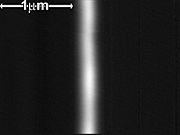
, photons of light fall on the entire cell, thus delivering energy and creating electron hole pairs, and cause a current to flow. In EBIC, energetic electrons take the role of the photons, causing the EBIC current to flow. However, because the electron beam of an SEM or STEM is very small, it is scanned across the sample and variations in the induced EBIC are used to map the electronic activity of the sample.

As such, EBIC is a semiconductor analysis technique useful for evaluating minority carrier properties and defect populations.
EBIC has also been extended to the study of local defects in insulators. For example, W.S. Lau (Lau Wai Shing
Lau Wai Shing
Wai Shing Lau is also known as Lau Wai Shing. Lau is an electrical engineer and also materials scientist. He worked on both Si-based and III-V based microelectronics.-Biography:...
) developed "true oxide electron beam induced current" in the 1990s. Thus, besides p-n junction
P-n junction
A p–n junction is formed at the boundary between a P-type and N-type semiconductor created in a single crystal of semiconductor by doping, for example by ion implantation, diffusion of dopants, or by epitaxy .If two separate pieces of material were used, this would...
or Schottky junction
Schottky diode
The Schottky diode is a semiconductor diode with a low forward voltage drop and a very fast switching action...
, EBIC can also be applied to MOS diodes. Local defects in semiconductor
Semiconductor
A semiconductor is a material with electrical conductivity due to electron flow intermediate in magnitude between that of a conductor and an insulator. This means a conductivity roughly in the range of 103 to 10−8 siemens per centimeter...
and local defects in the insulator could be distinguished. There exists a kind of defect which originates in the silicon
Silicon
Silicon is a chemical element with the symbol Si and atomic number 14. A tetravalent metalloid, it is less reactive than its chemical analog carbon, the nonmetal directly above it in the periodic table, but more reactive than germanium, the metalloid directly below it in the table...
substrate and extends into the insulator on top of the silicon
Silicon
Silicon is a chemical element with the symbol Si and atomic number 14. A tetravalent metalloid, it is less reactive than its chemical analog carbon, the nonmetal directly above it in the periodic table, but more reactive than germanium, the metalloid directly below it in the table...
substrate. (Please see references below.)
Recently, EBIC has been applied to high-k dielectric
High-k Dielectric
The term high-κ dielectric refers to a material with a high dielectric constant κ used in semiconductor manufacturing processes which replaces the silicon dioxide gate dielectric...
used in advanced CMOS
CMOS
Complementary metal–oxide–semiconductor is a technology for constructing integrated circuits. CMOS technology is used in microprocessors, microcontrollers, static RAM, and other digital logic circuits...
technology. (Please see references below.)