
Dynamic random access memory
Encyclopedia
Dynamic random-access memory (DRAM) is a type of random-access memory
that stores each bit
of data in a separate capacitor
within an integrated circuit
. The capacitor can be either charged or discharged; these two states are taken to represent the two values of a bit, conventionally called 0 and 1. Since capacitors leak charge, the information eventually fades unless the capacitor charge is refreshed
periodically. Because of this refresh requirement, it is a dynamic memory as opposed to SRAM
and other static memory.
The main memory (the "RAM") in personal computers is Dynamic RAM (DRAM). It is the RAM in laptop
, notebook
and workstation
computers as well as some of the RAM of home game consoles (PlayStation3, Xbox 360
and Wii
),
The advantage of DRAM is its structural simplicity: only one transistor and a capacitor are required per bit, compared to six transistors in SRAM. This allows DRAM to reach very high densities
. Unlike flash memory
, DRAM is volatile memory
(cf. non-volatile memory
), since it loses its data quickly when power is removed. The transistors and capacitors used are extremely small; billions can fit on a single memory chip.
machine code-named "Aquarius" used at Bletchley Park
during World War II
incorporated a hard-wired dynamic memory. Paper tape was read and the characters on it "were remembered in a dynamic store. ... The store used a large bank of capacitors, which were either charged or not, a charged capacitor representing cross (1) and an uncharged capacitor dot (0). Since the charge gradually leaked away, a periodic pulse was applied to top up those still charged (hence the term 'dynamic')".
 In 1964 Arnold Farber and Eugene Schlig, working for IBM, created a hard-wired memory cell, using a transistor gate and tunnel diode latch. They replaced the latch with two transistors and two resistors, a configuration which became known as the Farber-Schlig cell.
In 1965 Benjamin Agusta and his team at IBM created a 16-bit silicon memory chip based on the Farber-Schlig cell, with 80 transistors, 64 resistors, and four diodes.
In 1966 DRAM was invented by Dr. Robert Dennard
at the IBM
Thomas J. Watson Research Center
. He was granted U.S. patent number 3,387,286 in 1968. Capacitors had been used for earlier memory schemes such as the drum of the Atanasoff–Berry Computer, the Williams tube
and the Selectron tube
.
The Toshiba "Toscal" BC-1411 electronic calculator, which was introduced in November 1966, used a form of dynamic RAM built from discrete components.
In 1969 Honeywell
asked Intel to make a DRAM using a 3-transistor
cell that they had developed. This became the Intel 1102 (1024x1) in early 1970. However, the 1102 had many problems, prompting Intel to begin work on their own improved design, in secrecy to avoid conflict with Honeywell. This became the first commercially-available DRAM memory, the Intel 1103 (1024x1), in October 1970, despite initial problems with low yield until the fifth revision of the mask
s. The 1103 was designed by Joel Karp and laid out by Barbara Maness.
The first DRAM with multiplexed row and column address lines was the Mostek
MK4096 (4096x1) designed by Robert Proebsting and introduced in 1973. This addressing scheme, a radical advance, enabled it to fit into packages with fewer pins, a cost advantage that grew with every jump in memory size. The MK4096 proved to be a very robust design for customer applications. At the 16K density, the cost advantage increased; the Mostek MK4116 16K DRAM, introduced in 1976, achieved greater than 75% worldwide DRAM market share. However, as density increased to 64K in the early 80s, Mostek was overtaken by Japanese DRAM manufacturers selling higher quality DRAMs using the same multiplexing scheme at below-cost prices.
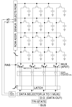
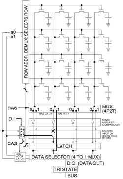 DRAM is usually arranged in a square array of one capacitor and transistor per data bit storage cell. The illustrations to the right show a simple example with 4 by 4 cells (modern DRAM matrices are many thousands of cells in height and width).
The long horizontal lines connecting each row are known as word Lines. Each column of cells is actually composed of two bit lines, each one connected to every other storage cell in the column (the illustration to the right does not include this important detail). They are generally known as the + and − bit lines. A sense amplifier is essentially a pair of cross-connected inverter
s between the bit lines, with the first inverter connected from the + bit line to the − bit line, and the second from the − bit line to the + bit line. This is an example of positive feedback
, and the arrangement is only stable after one bit line is high and one bit line is low.
To read a bit from a column, the following operations take place:
To write to memory, the row is opened and a given column's sense amplifier is temporarily forced to the desired high or low voltage state, thus it drives the bit line to charge or discharge the cell storage capacitor to the desired value. Due to positive feedback, the amplifier will then hold it stable even after the forcing is removed. During a write to a particular cell, all the columns in a row are sensed simultaneously just as in reading, a single column's cell storage capacitor charge is changed, and then the entire row is written back in, as illustrated in the figure to the right.
Typically, manufacturers specify that each row must have its storage cell capacitors refreshed every 64 ms or less, as defined by the JEDEC
(Foundation for developing Semiconductor Standards) standard. Refresh logic is provided in a DRAM controller which automates the periodic refresh, that is no software or other hardware has to perform it. This makes the controller's logic circuit more complicated, but this drawback is outweighed by the fact that DRAM is much cheaper per storage cell and because each storage cell is very simple, DRAM has much greater capacity per geographic area than SRAM.
Some systems refresh every row in a burst of activity involving all rows every 64 ms. Other systems refresh one row at a time staggered throughout the 64 ms interval. For example, a system with 213 = 8192 rows would require a staggered refresh rate
of one row every 7.8 µs which is 64 ms divided by 8192 rows. A few real-time systems refresh a portion of memory at a time determined by an external timer function that governs the operation of the rest of a system, such as the vertical blanking interval
that occurs every 10–20 ms in video equipment. All methods require some sort of counter to keep track of which row is the next to be refreshed. Most DRAM chips include that counter. Older types require external refresh logic to hold the counter (under some conditions, most of the data in DRAM can be recovered even if the DRAM has not been refreshed for several minutes).
Thus, the generally quoted number is the /RAS access time. This is the time to read a random bit from a precharged DRAM array. The time to read additional bits from an open page is much less.
When such a RAM is accessed by clocked logic, the times are generally rounded up to the nearest clock cycle. For example, when accessed by a 100 MHz state machine (i.e. a 10 ns clock), the 50 ns DRAM can perform the first read in five clock cycles, and additional reads within the same page every two clock cycles. This was generally described as timing, as bursts of four reads within a page were common.
When describing synchronous memory, timing is described by clock cycle counts separated by hyphens. These numbers represent in multiples of the DRAM clock cycle time. Note that this is half of the data transfer rate when double data rate
signaling is used. JEDEC standard PC3200 timing is with a 200 MHz clock, while premium-priced high performance PC3200 DDR DRAM DIMM might be operated at timing.
The improvement over 11 years is not that significant. Minimum random access time has improved from tRAC = 50 ns to , and even the premium 20 ns variety is only 2.5 times better. CAS latency
has improved even less, from to 10 ns. However, the DDR3 memory does achieve 32 times higher bandwidth; due to internal pipelining and wide data paths, it can output two words every 1.25 ns , while the EDO DRAM can output one word per tPC = 20 ns (50 Mword/s).
") errors in DRAM chips occur as a result of background radiation
, chiefly neutron
s from cosmic ray
secondaries, which may change the contents of one or more memory cells or interfere with the circuitry used to read/write them. Recent studies show that single event upset
s due to cosmic radiation have been dropping dramatically with process geometry and previous concerns over increasing bit cell error rates are unfounded.
This problem can be mitigated by using redundant
memory bits and memory controllers that exploit these bits, usually implemented within DRAM modules. These extra bits are used to record parity
and to enable missing data to be reconstructed by error-correcting code (ECC). Parity allows the detection of all single-bit errors (actually, any odd number of wrong bits). The most common error-correcting code, a SECDED Hamming code, allows a single-bit error to be corrected and, in the usual configuration, with an extra parity bit, double-bit errors to be detected.
An ECC-capable memory controller as used in many modern PCs can typically detect and correct errors of a single bit per 64-bit "word" (the unit of bus
transfer), and detect (but not correct) errors of two bits per 64-bit word. Some systems also 'scrub' the errors, by writing the corrected version back to memory. The BIOS
in some computers, and operating systems such as Linux
, allow counting of detected and corrected memory errors; this allows identification and replacement of failing memory modules.
Recent tests give widely varying error rates with over 7 orders of magnitude difference, ranging from , roughly one bit error, per hour, per gigabyte of memory to one bit error, per century, per gigabyte of memory.
).
s (ICs) bonded
and mounted into plastic packages with metal pins for connection to control signals and buses. In early use individual DRAM ICs were usually either installed directly to the motherboard
or on ISA
expansion cards; later they were assembled into multi-chip plug-in modules (DIMMs, SIMMs, etc.). Some standard module types are:

This interface provides direct control of internal timing. When /RAS is driven low, a /CAS cycle must not be attempted until the sense amplifiers have sensed the memory state, and /RAS must not be returned high until the storage cells have been refreshed. When /RAS is driven high, it must be held high long enough for precharging to complete.
Although the RAM is asynchronous, the signals are typically generated by a clocked memory controller, which limits their timing to multiples of the controller's clock cycle.
The refresh cycles are distributed across the entire refresh interval in such a way that all rows are refreshed within the required interval. To refresh one row of the memory array using /RAS Only Refresh, the following steps must occur:
1. The row address of the row to be refreshed must be applied at the address input pins.
2. /RAS must switch from high to low. /CAS must remain high.
3. At the end of the required amount of time, /RAS must return high.
This can be done by supplying a row address and pulsing /RAS low; it is not necessary to perform any /CAS cycles. An external counter is needed to iterate over the row addresses in turn.
This became the standard form of refresh for asynchronous DRAM, and is the only form generally used with SDRAM.
variant of DRAM that was once commonly used to store the frame-buffer in some graphics adaptors.
Fast page mode DRAM is also called FPM DRAM, FPRAM, Page mode DRAM, Fast page mode memory, or Page mode memory.
In page mode, a row of the DRAM can be kept "open" by holding /RAS low while performing multiple reads or writes with separate pulses of /CAS so that successive reads or writes within the row do not suffer the delay of precharge and accessing the row. This increases the performance of the system when reading or writing bursts of data.
Static column is a variant of page mode in which the column address does not need to be strobed in, but rather, the address inputs may be changed with /CAS held low, and the data output will be updated accordingly a few nanoseconds later.
Nibble mode is another variant in which four sequential locations within the row can be accessed with four consecutive pulses of /CAS. The difference from normal page mode is that the address inputs are not used for the second through fourth /CAS edges; they are generated internally starting with the address supplied for the first /CAS edge.
 EDO DRAM, sometimes referred to as Hyper Page Mode enabled DRAM, is similar to Fast Page Mode DRAM with the additional feature that a new access cycle can be started while keeping the data output of the previous cycle active. This allows a certain amount of overlap in operation (pipelining), allowing somewhat improved performance. It was 5% faster than FPM DRAM, which it began to replace in 1995, when Intel introduced the 430FX chipset that supported EDO DRAM.
To be precise, EDO DRAM begins data output on the falling edge of /CAS, but does not stop the output when /CAS rises again. It holds the output valid (thus extending the data output time) until either /RAS is deasserted, or a new /CAS falling edge selects a different column address.
Single-cycle EDO has the ability to carry out a complete memory transaction in one clock cycle. Otherwise, each sequential RAM access within the same page takes two clock cycles instead of three, once the page has been selected. EDO's performance and capabilities allowed it to somewhat replace the then-slow L2 caches of PCs. It created an opportunity to reduce the immense performance loss associated with a lack of L2 cache, while making systems cheaper to build. This was also good for notebooks due to difficulties with their limited form factor, and battery life limitations. An EDO system with L2 cache was tangibly faster than the older FPM/L2 combination.
Single-cycle EDO DRAM became very popular on video cards towards the end of the 1990s. It was very low cost, yet nearly as efficient for performance as the far more costly VRAM.
Much equipment taking 72-pin SIMMs could use either FPM or EDO. Problems were possible, particularly when mixing FPM and EDO. Early Hewlett-Packard
printers had FPM RAM built in; some, but not all, models worked if additional EDO SIMMs were added.
Although BEDO DRAM showed additional optimization over EDO, by the time it was available the market had made a significant investment towards synchronous DRAM, or SDRAM http://www.tomshardware.com/1998/10/24/ram_guide/page7.html. Even though BEDO RAM was superior to SDRAM in some ways, the latter technology quickly displaced BEDO.
technique for main memory to second-level cache
memory to provide a cheaper and faster alternative to SRAM
. The chip splits its memory capacity into small blocks of and allows operations to two different banks in a single clock cycle.
This memory was primarily used in graphic cards with Tseng Labs
ET6x00 chipsets, and was made by MoSys. Boards based upon this chipset often used the unusual RAM size configuration of , owing to MDRAM's ability to be implemented in various sizes more easily. This size of allowed 24-bit color at a resolution of 1024×768, a very popular display setting in the card's time.
Some DRAM components have a "self-refresh mode". While this involves much of the same logic that is needed for pseudo-static operation, this mode is often equivalent to a standby mode. It is provided primarily to allow a system to suspend operation of its DRAM controller to save power without losing data stored in DRAM, not to allow operation without a separate DRAM controller as is the case with PSRAM.
An embedded variant of PSRAM is sold by MoSys under the name 1T-SRAM
. It is technically DRAM, but behaves much like SRAM. It is used in Nintendo
Gamecube
and Wii
consoles.
transistors. Considered a nuisance in logic design, this floating body effect
can be used for data storage. Although refresh is still required, reads are non-destructive; the stored charge causes a detectable shift in the threshold voltage
of the transistor.
There are several types of 1T DRAM memories: the commercialized Z-RAM
from Innovative Silicon, the TTRAM
from Renesas and the A-RAM
from the UGR
/CNRS consortium. Faster versions of 1T DRAM are sometimes called 1T-SRAM
.
The classic one-transistor/one-capacitor (1T/1C) DRAM cell is also sometimes referred to as "1T DRAM".
This property can be used to circumvent security and recover data stored in memory and assumed to be destroyed at power-down by quickly rebooting the computer and dumping the contents of the RAM, or by cooling the chips and transferring them to a different computer. Such an attack was demonstrated to circumvent popular disk encryption systems, such as the open source
TrueCrypt
, Microsoft's BitLocker Drive Encryption
, and Apple's FileVault
. This type of attack against a computer is often called a cold boot attack
.
Random-access memory
Random access memory is a form of computer data storage. Today, it takes the form of integrated circuits that allow stored data to be accessed in any order with a worst case performance of constant time. Strictly speaking, modern types of DRAM are therefore not random access, as data is read in...
that stores each bit
Bit
A bit is the basic unit of information in computing and telecommunications; it is the amount of information stored by a digital device or other physical system that exists in one of two possible distinct states...
of data in a separate capacitor
Capacitor
A capacitor is a passive two-terminal electrical component used to store energy in an electric field. The forms of practical capacitors vary widely, but all contain at least two electrical conductors separated by a dielectric ; for example, one common construction consists of metal foils separated...
within an integrated circuit
Integrated circuit
An integrated circuit or monolithic integrated circuit is an electronic circuit manufactured by the patterned diffusion of trace elements into the surface of a thin substrate of semiconductor material...
. The capacitor can be either charged or discharged; these two states are taken to represent the two values of a bit, conventionally called 0 and 1. Since capacitors leak charge, the information eventually fades unless the capacitor charge is refreshed
Memory refresh
Memory refresh is the process of periodically reading information from an area of computer memory, and immediately rewriting the read information to the same area with no modifications. Each memory refresh cycle refreshes a succeeding area of memory. Memory refresh is most often associated with...
periodically. Because of this refresh requirement, it is a dynamic memory as opposed to SRAM
Static random access memory
Static random-access memory is a type of semiconductor memory where the word static indicates that, unlike dynamic RAM , it does not need to be periodically refreshed, as SRAM uses bistable latching circuitry to store each bit...
and other static memory.
The main memory (the "RAM") in personal computers is Dynamic RAM (DRAM). It is the RAM in laptop
Laptop
A laptop, also called a notebook, is a personal computer for mobile use. A laptop integrates most of the typical components of a desktop computer, including a display, a keyboard, a pointing device and speakers into a single unit...
, notebook
Laptop
A laptop, also called a notebook, is a personal computer for mobile use. A laptop integrates most of the typical components of a desktop computer, including a display, a keyboard, a pointing device and speakers into a single unit...
and workstation
Workstation
A workstation is a high-end microcomputer designed for technical or scientific applications. Intended primarily to be used by one person at a time, they are commonly connected to a local area network and run multi-user operating systems...
computers as well as some of the RAM of home game consoles (PlayStation3, Xbox 360
Xbox 360
The Xbox 360 is the second video game console produced by Microsoft and the successor to the Xbox. The Xbox 360 competes with Sony's PlayStation 3 and Nintendo's Wii as part of the seventh generation of video game consoles...
and Wii
Wii
The Wii is a home video game console released by Nintendo on November 19, 2006. As a seventh-generation console, the Wii primarily competes with Microsoft's Xbox 360 and Sony's PlayStation 3. Nintendo states that its console targets a broader demographic than that of the two others...
),
The advantage of DRAM is its structural simplicity: only one transistor and a capacitor are required per bit, compared to six transistors in SRAM. This allows DRAM to reach very high densities
Computer storage density
Memory storage density is a measure of the quantity of information bits that can be stored on a given length of track, area of surface, or in a given volume of a computer storage medium. Generally, higher density is more desirable, for it allows greater volumes of data to be stored in the same...
. Unlike flash memory
Flash memory
Flash memory is a non-volatile computer storage chip that can be electrically erased and reprogrammed. It was developed from EEPROM and must be erased in fairly large blocks before these can be rewritten with new data...
, DRAM is volatile memory
Volatile memory
Volatile memory, also known as volatile storage, is computer memory that requires power to maintain the stored information, unlike non-volatile memory which does not require a maintained power supply...
(cf. non-volatile memory
Non-volatile memory
Non-volatile memory, nonvolatile memory, NVM or non-volatile storage, in the most basic sense, is computer memory that can retain the stored information even when not powered. Examples of non-volatile memory include read-only memory, flash memory, ferroelectric RAM, most types of magnetic computer...
), since it loses its data quickly when power is removed. The transistors and capacitors used are extremely small; billions can fit on a single memory chip.
History
The cryptanalyticCryptanalysis
Cryptanalysis is the study of methods for obtaining the meaning of encrypted information, without access to the secret information that is normally required to do so. Typically, this involves knowing how the system works and finding a secret key...
machine code-named "Aquarius" used at Bletchley Park
Bletchley Park
Bletchley Park is an estate located in the town of Bletchley, in Buckinghamshire, England, which currently houses the National Museum of Computing...
during World War II
World War II
World War II, or the Second World War , was a global conflict lasting from 1939 to 1945, involving most of the world's nations—including all of the great powers—eventually forming two opposing military alliances: the Allies and the Axis...
incorporated a hard-wired dynamic memory. Paper tape was read and the characters on it "were remembered in a dynamic store. ... The store used a large bank of capacitors, which were either charged or not, a charged capacitor representing cross (1) and an uncharged capacitor dot (0). Since the charge gradually leaked away, a periodic pulse was applied to top up those still charged (hence the term 'dynamic')".
In 1965 Benjamin Agusta and his team at IBM created a 16-bit silicon memory chip based on the Farber-Schlig cell, with 80 transistors, 64 resistors, and four diodes.
In 1966 DRAM was invented by Dr. Robert Dennard
Robert Dennard
Robert Dennard is an American electrical engineer and inventor.Dennard was born in Terrell, Texas, U.S.. He received his B.S. and M.S. degrees in Electrical Engineering from Southern Methodist University, Dallas, in 1954 and 1956, respectively. He earned a Ph.D. from Carnegie Institute of...
at the IBM
IBM
International Business Machines Corporation or IBM is an American multinational technology and consulting corporation headquartered in Armonk, New York, United States. IBM manufactures and sells computer hardware and software, and it offers infrastructure, hosting and consulting services in areas...
Thomas J. Watson Research Center
Thomas J. Watson Research Center
The Thomas J. Watson Research Center is the headquarters for the IBM Research Division.The center is on three sites, with the main laboratory in Yorktown Heights, New York, 38 miles north of New York City, a building in Hawthorne, New York, and offices in Cambridge, Massachusetts.- Overview :The...
. He was granted U.S. patent number 3,387,286 in 1968. Capacitors had been used for earlier memory schemes such as the drum of the Atanasoff–Berry Computer, the Williams tube
Williams tube
The Williams tube or the Williams-Kilburn tube , developed in about 1946 or 1947, was a cathode ray tube used to electronically store binary data....
and the Selectron tube
Selectron tube
The Selectron was an early form of digital computer memory developed by Jan A. Rajchman and his group at the Radio Corporation of America under the direction of Vladimir Zworykin, of television technology fame...
.
The Toshiba "Toscal" BC-1411 electronic calculator, which was introduced in November 1966, used a form of dynamic RAM built from discrete components.
In 1969 Honeywell
Honeywell
Honeywell International, Inc. is a major conglomerate company that produces a variety of consumer products, engineering services, and aerospace systems for a wide variety of customers, from private consumers to major corporations and governments....
asked Intel to make a DRAM using a 3-transistor
Transistor
A transistor is a semiconductor device used to amplify and switch electronic signals and power. It is composed of a semiconductor material with at least three terminals for connection to an external circuit. A voltage or current applied to one pair of the transistor's terminals changes the current...
cell that they had developed. This became the Intel 1102 (1024x1) in early 1970. However, the 1102 had many problems, prompting Intel to begin work on their own improved design, in secrecy to avoid conflict with Honeywell. This became the first commercially-available DRAM memory, the Intel 1103 (1024x1), in October 1970, despite initial problems with low yield until the fifth revision of the mask
Photomask
A photomask is an opaque plate with holes or transparencies that allow light to shine through in a defined pattern. They are commonly used in photolithography.-Overview:...
s. The 1103 was designed by Joel Karp and laid out by Barbara Maness.
The first DRAM with multiplexed row and column address lines was the Mostek
Mostek
Mostek was an integrated circuit manufacturer, founded in 1969 by ex-employees of Texas Instruments. Initially their products were manufactured in Worcester, Massachusetts, however by 1974 most of its manufacturing was done in the Carrollton, Texas facility on Crosby Road...
MK4096 (4096x1) designed by Robert Proebsting and introduced in 1973. This addressing scheme, a radical advance, enabled it to fit into packages with fewer pins, a cost advantage that grew with every jump in memory size. The MK4096 proved to be a very robust design for customer applications. At the 16K density, the cost advantage increased; the Mostek MK4116 16K DRAM, introduced in 1976, achieved greater than 75% worldwide DRAM market share. However, as density increased to 64K in the early 80s, Mostek was overtaken by Japanese DRAM manufacturers selling higher quality DRAMs using the same multiplexing scheme at below-cost prices.
Operation principle
The long horizontal lines connecting each row are known as word Lines. Each column of cells is actually composed of two bit lines, each one connected to every other storage cell in the column (the illustration to the right does not include this important detail). They are generally known as the + and − bit lines. A sense amplifier is essentially a pair of cross-connected inverter
Inverter (logic gate)
In digital logic, an inverter or NOT gate is a logic gate which implements logical negation. The truth table is shown on the right.This represents perfect switching behavior, which is the defining assumption in Digital electronics. In practice, actual devices have electrical characteristics that...
s between the bit lines, with the first inverter connected from the + bit line to the − bit line, and the second from the − bit line to the + bit line. This is an example of positive feedback
Positive feedback
Positive feedback is a process in which the effects of a small disturbance on a system include an increase in the magnitude of the perturbation. That is, A produces more of B which in turn produces more of A. In contrast, a system that responds to a perturbation in a way that reduces its effect is...
, and the arrangement is only stable after one bit line is high and one bit line is low.
To read a bit from a column, the following operations take place:
- The sense amplifier is disconnected, then the bit lines are precharged to exactly equal voltages that are in-between high and low logic levels. The bit lines are physically symmetrical to keep the capacitance as equal and therefore the voltages as equal as possible.
- The precharge circuit is switched off. Because the bit lines are relatively long, they have enough capacitanceCapacitanceIn electromagnetism and electronics, capacitance is the ability of a capacitor to store energy in an electric field. Capacitance is also a measure of the amount of electric potential energy stored for a given electric potential. A common form of energy storage device is a parallel-plate capacitor...
to maintain the pre-charged voltage for a brief time. This is an example of dynamic logicDynamic logic (digital logic)In integrated circuit design, dynamic logic is a design methodology in combinatorial logic circuits, particularly those implemented in MOS technology. It is distinguished from the so-called static logic by exploiting temporary storage of information in stray and gate capacitances...
. - The desired row's word line is then driven high to connect a cell's storage capacitor to its bit line. This causes the transistor to conduct, transferring chargeElectric chargeElectric charge is a physical property of matter that causes it to experience a force when near other electrically charged matter. Electric charge comes in two types, called positive and negative. Two positively charged substances, or objects, experience a mutual repulsive force, as do two...
between the storage cell and the connected bit line. If the storage cell capacitor is discharged, it will greatly decrease the voltage on the bit-line as the precharge is transferred to the storage capacitor. If the storage cell is charged, the bit-line voltage decreases only slightly; this is because every effort is made to keep the capacitance of the storage cells high and the capacitance of the bit lines low. - The sense amplifier is switched on. The positive feedback takes over and amplifies the small voltage difference between bit-lines until one bit line is fully at the lowest voltage and the other is at the maximum high voltage. Once this has happened, the row is "open" (the desired cell data is available).
- All columns are sensed in simultaneously and the result sampled into the data latch. A provided Column address then selects which latch bit to connect to the external circuit. Many reads can be performed quickly without delay sense for the open row, all data has already been sensed and latched.
- While reading all columns proceeds (the normal and desirable method because it most quickly provides data), current is flowing back up the bit lines from the sense amplifiers to the storage cells. This reinforces (i.e. "refreshes") the charge in the storage cell by increasing the voltage in the storage capacitor if it was charged to begin with, or by keeping it discharged if it was empty. Note that due to the length of the bit lines creating a fairly long propagation delay for the charge to be transferred, this takes significant time beyond the end of sense amplification, and thus overlaps with one or more column reads.
- When done with the reading all the columns in the current row, the word line is switched off to disconnect the cell storage capacitors (the row is "closed"), the sense amplifier is switched off, and the bit lines are precharged again.
To write to memory, the row is opened and a given column's sense amplifier is temporarily forced to the desired high or low voltage state, thus it drives the bit line to charge or discharge the cell storage capacitor to the desired value. Due to positive feedback, the amplifier will then hold it stable even after the forcing is removed. During a write to a particular cell, all the columns in a row are sensed simultaneously just as in reading, a single column's cell storage capacitor charge is changed, and then the entire row is written back in, as illustrated in the figure to the right.
Typically, manufacturers specify that each row must have its storage cell capacitors refreshed every 64 ms or less, as defined by the JEDEC
JEDEC
The JEDEC Solid State Technology Association, formerly known as the Joint Electron Devices Engineering Council , is an independent semiconductor engineering trade organization and standardization body...
(Foundation for developing Semiconductor Standards) standard. Refresh logic is provided in a DRAM controller which automates the periodic refresh, that is no software or other hardware has to perform it. This makes the controller's logic circuit more complicated, but this drawback is outweighed by the fact that DRAM is much cheaper per storage cell and because each storage cell is very simple, DRAM has much greater capacity per geographic area than SRAM.
Some systems refresh every row in a burst of activity involving all rows every 64 ms. Other systems refresh one row at a time staggered throughout the 64 ms interval. For example, a system with 213 = 8192 rows would require a staggered refresh rate
Refresh rate
The refresh rate is the number of times in a second that a display hardware draws the data...
of one row every 7.8 µs which is 64 ms divided by 8192 rows. A few real-time systems refresh a portion of memory at a time determined by an external timer function that governs the operation of the rest of a system, such as the vertical blanking interval
Vertical blanking interval
The vertical blanking interval , also known as the vertical interval or VBLANK, is the time difference between the last line of one frame or field of a raster display, and the beginning of the first line of the next frame. It is present in analog television, VGA, DVI and other signals. During the...
that occurs every 10–20 ms in video equipment. All methods require some sort of counter to keep track of which row is the next to be refreshed. Most DRAM chips include that counter. Older types require external refresh logic to hold the counter (under some conditions, most of the data in DRAM can be recovered even if the DRAM has not been refreshed for several minutes).
Memory timing
Many parameters are required to fully describe the timing of DRAM operation. Here are some examples for two timing grades of asynchronous DRAM, from a data sheet published in 1998:| "50 ns" | "60 ns" | Description | |
| tRC | 84 ns | 104 ns | Random read or write cycle time (from one full /RAS cycle to another) |
| tRAC | 50 ns | 60 ns | Access time: /RAS low to valid data out |
| tRCD | 11 ns | 14 ns | /RAS low to /CAS low time |
| tRAS | 50 ns | 60 ns | /RAS pulse width (minimum /RAS low time) |
| tRP | 30 ns | 40 ns | /RAS precharge time (minimum /RAS high time) |
| tPC | 20 ns | 25 ns | Page-mode read or write cycle time (/CAS to /CAS) |
| tAA | 25 ns | 30 ns | Access time: Column address valid to valid data out (includes address setup time before /CAS low) |
| tCAC | 13 ns | 15 ns | Access time: /CAS low to valid data out |
| tCAS | 8 ns | 10 ns | /CAS low pulse width minimum |
Thus, the generally quoted number is the /RAS access time. This is the time to read a random bit from a precharged DRAM array. The time to read additional bits from an open page is much less.
When such a RAM is accessed by clocked logic, the times are generally rounded up to the nearest clock cycle. For example, when accessed by a 100 MHz state machine (i.e. a 10 ns clock), the 50 ns DRAM can perform the first read in five clock cycles, and additional reads within the same page every two clock cycles. This was generally described as timing, as bursts of four reads within a page were common.
When describing synchronous memory, timing is described by clock cycle counts separated by hyphens. These numbers represent in multiples of the DRAM clock cycle time. Note that this is half of the data transfer rate when double data rate
Double data rate
In computing, a computer bus operating with double data rate transfers data on both the rising and falling edges of the clock signal. This is also known as double pumped, dual-pumped, and double transition....
signaling is used. JEDEC standard PC3200 timing is with a 200 MHz clock, while premium-priced high performance PC3200 DDR DRAM DIMM might be operated at timing.
| PC-3200 (DDR-400) | PC2-6400 (DDR2-800) | PC3-12800 (DDR3-1600) | Description | ||||||||||
| Typical | Fast | Typical | Fast | Typical | Fast | ||||||||
| cycles | time | cycles | time | cycles | time | cycles | time | cycles | time | cycles | time | ||
| tCL | 3 | 15 ns | 2 | 10 ns | 5 | 12.5 ns | 4 | 10 ns | 9 | 11.25 ns | 8 | 10 ns | /CAS low to valid data out (equivalent to tCAC) |
| tRCD | 4 | 20 ns | 2 | 10 ns | 5 | 12.5 ns | 4 | 10 ns | 9 | 11.25 ns | 8 | 10 ns | /RAS low to /CAS low time |
| tRP | 4 | 20 ns | 2 | 10 ns | 5 | 12.5 ns | 4 | 10 ns | 9 | 11.25 ns | 8 | 10 ns | /RAS precharge time (minimum precharge to active time) |
| tRAS | 8 | 40 ns | 5 | 25 ns | 16 | 40 ns | 12 | 30 ns | 27 | 33.75 ns | 24 | 30 ns | Row active time (minimum active to precharge time) |
The improvement over 11 years is not that significant. Minimum random access time has improved from tRAC = 50 ns to , and even the premium 20 ns variety is only 2.5 times better. CAS latency
CAS Latency
Column Address Strobe latency, or CL, is the delay time between the moment a memory controller tells the memory module to access a particular memory column on a RAM memory module, and the moment the data from given array location is available on the module's output pins...
has improved even less, from to 10 ns. However, the DDR3 memory does achieve 32 times higher bandwidth; due to internal pipelining and wide data paths, it can output two words every 1.25 ns , while the EDO DRAM can output one word per tPC = 20 ns (50 Mword/s).
Timing abbreviations
|
|
Error detection and correction
Electrical or magnetic interference inside a computer system can cause a single bit of DRAM to spontaneously flip to the opposite state. The majority of one-off ("softSoft error
In electronics and computing, a soft error is an error in a signal or datum which is wrong. Errors may be caused by a defect, usually understood either to be a mistake in design or construction, or a broken component. A soft error is also a signal or datum which is wrong, but is not assumed to...
") errors in DRAM chips occur as a result of background radiation
Background radiation
Background radiation is the ionizing radiation constantly present in the natural environment of the Earth, which is emitted by natural and artificial sources.-Overview:Both Natural and human-made background radiation varies by location....
, chiefly neutron
Neutron
The neutron is a subatomic hadron particle which has the symbol or , no net electric charge and a mass slightly larger than that of a proton. With the exception of hydrogen, nuclei of atoms consist of protons and neutrons, which are therefore collectively referred to as nucleons. The number of...
s from cosmic ray
Cosmic ray
Cosmic rays are energetic charged subatomic particles, originating from outer space. They may produce secondary particles that penetrate the Earth's atmosphere and surface. The term ray is historical as cosmic rays were thought to be electromagnetic radiation...
secondaries, which may change the contents of one or more memory cells or interfere with the circuitry used to read/write them. Recent studies show that single event upset
Single event upset
A single event upset is a change of state caused by ions or electro-magnetic radiation striking a sensitive node in a micro-electronic device, such as in a microprocessor, semiconductor memory, or power transistors. The state change is a result of the free charge created by ionization in or close...
s due to cosmic radiation have been dropping dramatically with process geometry and previous concerns over increasing bit cell error rates are unfounded.
This problem can be mitigated by using redundant
Redundancy (engineering)
In engineering, redundancy is the duplication of critical components or functions of a system with the intention of increasing reliability of the system, usually in the case of a backup or fail-safe....
memory bits and memory controllers that exploit these bits, usually implemented within DRAM modules. These extra bits are used to record parity
RAM parity
RAM parity checking is the storing of a redundant parity bit representing the parity of a small amount of computer data stored in random access memory, and the subsequent comparison of the stored and the computed parity to detect whether a data error has occurred.The parity bit was originally...
and to enable missing data to be reconstructed by error-correcting code (ECC). Parity allows the detection of all single-bit errors (actually, any odd number of wrong bits). The most common error-correcting code, a SECDED Hamming code, allows a single-bit error to be corrected and, in the usual configuration, with an extra parity bit, double-bit errors to be detected.
An ECC-capable memory controller as used in many modern PCs can typically detect and correct errors of a single bit per 64-bit "word" (the unit of bus
Computer bus
In computer architecture, a bus is a subsystem that transfers data between components inside a computer, or between computers.Early computer buses were literally parallel electrical wires with multiple connections, but the term is now used for any physical arrangement that provides the same...
transfer), and detect (but not correct) errors of two bits per 64-bit word. Some systems also 'scrub' the errors, by writing the corrected version back to memory. The BIOS
BIOS
In IBM PC compatible computers, the basic input/output system , also known as the System BIOS or ROM BIOS , is a de facto standard defining a firmware interface....
in some computers, and operating systems such as Linux
Linux
Linux is a Unix-like computer operating system assembled under the model of free and open source software development and distribution. The defining component of any Linux system is the Linux kernel, an operating system kernel first released October 5, 1991 by Linus Torvalds...
, allow counting of detected and corrected memory errors; this allows identification and replacement of failing memory modules.
Recent tests give widely varying error rates with over 7 orders of magnitude difference, ranging from , roughly one bit error, per hour, per gigabyte of memory to one bit error, per century, per gigabyte of memory.
Packaging
For economic reasons, the large (main) memories found in personal computers, workstations, and non-handheld game-consoles (such as PlayStation and Xbox) normally consist of dynamic RAM (DRAM). Other parts of the computer, such as cache memories and data buffers in hard disks, normally use static RAM (SRAMStatic random access memory
Static random-access memory is a type of semiconductor memory where the word static indicates that, unlike dynamic RAM , it does not need to be periodically refreshed, as SRAM uses bistable latching circuitry to store each bit...
).
General DRAM formats
Dynamic random access memory is produced as integrated circuitIntegrated circuit
An integrated circuit or monolithic integrated circuit is an electronic circuit manufactured by the patterned diffusion of trace elements into the surface of a thin substrate of semiconductor material...
s (ICs) bonded
Adhesive
An adhesive, or glue, is a mixture in a liquid or semi-liquid state that adheres or bonds items together. Adhesives may come from either natural or synthetic sources. The types of materials that can be bonded are vast but they are especially useful for bonding thin materials...
and mounted into plastic packages with metal pins for connection to control signals and buses. In early use individual DRAM ICs were usually either installed directly to the motherboard
Motherboard
In personal computers, a motherboard is the central printed circuit board in many modern computers and holds many of the crucial components of the system, providing connectors for other peripherals. The motherboard is sometimes alternatively known as the mainboard, system board, or, on Apple...
or on ISA
Industry Standard Architecture
Industry Standard Architecture is a computer bus standard for IBM PC compatible computers introduced with the IBM Personal Computer to support its Intel 8088 microprocessor's 8-bit external data bus and extended to 16 bits for the IBM Personal Computer/AT's Intel 80286 processor...
expansion cards; later they were assembled into multi-chip plug-in modules (DIMMs, SIMMs, etc.). Some standard module types are:
- DRAM chip (Integrated Circuit or IC)
- Dual in-line Package (DIPDual in-line packageIn microelectronics, a dual in-line package is an electronic device package with a rectangular housing and two parallel rows of electrical connecting pins. The package may be through-hole mounted to a printed circuit board or inserted in a socket.A DIP is usually referred to as a DIPn, where n is...
)
- Dual in-line Package (DIP
- DRAM (memory) modules
- Single In-line Pin Package (SIPPSIPP memoryA SIPP or single in-line pin package was a type of random access memory.It consisted of a small printed circuit board upon which were mounted a number of memory chips. It had 30 pins along one edge which mated with matching holes in the motherboard of the computer.This type of memory was used in...
) - Single In-line Memory Module (SIMMSIMMA SIMM, or single in-line memory module, is a type of memory module containing random access memory used in computers from the early 1980s to the late 1990s. It differs from a dual in-line memory module , the most predominant form of memory module today, in that the contacts on a SIMM are redundant...
) - Dual In-line Memory Module (DIMMDIMMA DIMM or dual in-line memory module, comprises a series of dynamic random-access memory integrated circuits. These modules are mounted on a printed circuit board and designed for use in personal computers, workstations and servers...
) - Rambus In-line Memory Module (RIMMRDRAMDirect Rambus DRAM or DRDRAM is a type of synchronous dynamic RAM. RDRAM was developed by Rambus inc., in the mid-1990s as a replacement for then-prevalent DIMM SDRAM memory architecture....
), technically DIMMDIMMA DIMM or dual in-line memory module, comprises a series of dynamic random-access memory integrated circuits. These modules are mounted on a printed circuit board and designed for use in personal computers, workstations and servers...
s but called RIMMs due to their proprietary slot. - Small outline DIMM (SO-DIMMSO-DIMMA SO-DIMM, or small outline dual in-line memory module, is a type of computer memory built using integrated circuits.SO-DIMMs are a smaller alternative to a DIMM, being roughly half the size of regular DIMMs...
), about half the size of regular DIMMs, are mostly used in notebooks, small footprint PCs (such as Mini-ITXMini-ITXMini-ITX is a 17 x 17 cm low-power motherboard form factor developed by VIA Technologies in 2001. Mini-ITX is slightly smaller than microATX. Mini-ITX boards can often be passively cooled due to their low power consumption architecture, which makes them useful for home theater PC systems,...
motherboards), upgradable office printers and networking hardware like routers. Comes in versions with:- 72-pin (32-bit)
- 144-pin (64-bit) used for SDRAMSDRAMSynchronous dynamic random access memory is dynamic random access memory that is synchronized with the system bus. Classic DRAM has an asynchronous interface, which means that it responds as quickly as possible to changes in control inputs...
- 200-pin (72-bit) used for DDR SDRAMDDR SDRAMDouble data rate synchronous dynamic random access memory is a class of memory integrated circuits used in computers. DDR SDRAM has been superseded by DDR2 SDRAM and DDR3 SDRAM, neither of which are either forward or backward compatible with DDR SDRAM, meaning that DDR2 or DDR3 memory modules...
and DDR2 SDRAMDDR2 SDRAMDDR2 SDRAM is a double data rate synchronous dynamic random-access memory interface. It supersedes the original DDR SDRAM specification and has itself been superseded by DDR3 SDRAM... - 204-pin (64-bit) used for DDR3 SDRAMDDR3 SDRAMIn computing, DDR3 SDRAM, an abbreviation for double data rate type three synchronous dynamic random access memory, is a modern kind of dynamic random access memory with a high bandwidth interface. It is one of several variants of DRAM and associated interface techniques used since the early 1970s...
- Small outline RIMM (SO-RIMM). Smaller version of the RIMM, used in laptops. Technically SO-DIMMs but called SO-RIMMs due to their proprietary slot.
- Single In-line Pin Package (SIPP
- Stacked vs. non-stacked RAM modules
- Stacked RAM modules contain two or more RAM chips stacked on top of each other. This allows large modules to be manufactured using cheaper low density wafers. Stacked chip modules draw more power, and tend to run hotter than non-stacked modules. Stacked modules can be built using the older TSOPThin small-outline packageThin small-outline packages, or TSOPs are a type of surface mount IC package. They are notably very low-profile and have tight lead spacing ....
or the newer BGABall grid arrayA ball grid array is a type of surface-mount packaging used for integrated circuits.- Description :The BGA is descended from the pin grid array , which is a package with one face covered with pins in a grid pattern. These pins conduct electrical signals from the integrated circuit to the printed...
style IC chips.
- Stacked RAM modules contain two or more RAM chips stacked on top of each other. This allows large modules to be manufactured using cheaper low density wafers. Stacked chip modules draw more power, and tend to run hotter than non-stacked modules. Stacked modules can be built using the older TSOP
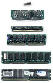
Common DRAM modules
Common DRAM packages as illustrated to the right, from top to bottom:- DIP 16-pin (DRAM chip, usually pre-fast page mode DRAM (FPRAM)
- SIPP 30-pin (usually FPRAM)
- SIMM 30-pin (usually FPRAM)
- SIMM 72-pin (often extended data out DRAM (EDO DRAM) but FPRAM is not uncommon)
- DIMM 168-pin (SDRAMSDRAMSynchronous dynamic random access memory is dynamic random access memory that is synchronized with the system bus. Classic DRAM has an asynchronous interface, which means that it responds as quickly as possible to changes in control inputs...
) - DIMM 184-pin (DDR SDRAMDDR SDRAMDouble data rate synchronous dynamic random access memory is a class of memory integrated circuits used in computers. DDR SDRAM has been superseded by DDR2 SDRAM and DDR3 SDRAM, neither of which are either forward or backward compatible with DDR SDRAM, meaning that DDR2 or DDR3 memory modules...
) - RIMM 184-pin (RDRAMRDRAMDirect Rambus DRAM or DRDRAM is a type of synchronous dynamic RAM. RDRAM was developed by Rambus inc., in the mid-1990s as a replacement for then-prevalent DIMM SDRAM memory architecture....
) not pictured - DIMM 240-pin (DDR2 SDRAMDDR2 SDRAMDDR2 SDRAM is a double data rate synchronous dynamic random-access memory interface. It supersedes the original DDR SDRAM specification and has itself been superseded by DDR3 SDRAM...
and DDR3 SDRAMDDR3 SDRAMIn computing, DDR3 SDRAM, an abbreviation for double data rate type three synchronous dynamic random access memory, is a modern kind of dynamic random access memory with a high bandwidth interface. It is one of several variants of DRAM and associated interface techniques used since the early 1970s...
) not pictured
Versions
While the fundamental DRAM cell and array has maintained the same basic structure (and performance) for many years, there have been many different interfaces for communicating with DRAM chips. When one speaks about "DRAM types", one is generally referring to the interface that is used.Asynchronous DRAM
This is the basic form from which all others derive. An asynchronous DRAM chip has power connections, some number of address inputs (typically 12), and a few (typically one or four) bidirectional data lines. There are four active-low control signals:- /RAS, the Row Address Strobe. The address inputs are captured on the falling edge of /RAS, and select a row to open. The row is held open as long as /RAS is low.
- /CAS, the Column Address Strobe. The address inputs are captured on the falling edge of /CAS, and select a column from the currently open row to read or write.
- /WE, Write Enable. This signal determines whether a given falling edge of /CAS is a read (if high) or write (if low). If low, the data inputs are also captured on the falling edge of /CAS.
- /OE, Output Enable. This is an additional signal that controls output to the data I/O pins. The data pins are driven by the DRAM chip if /RAS and /CAS are low, /WE is high, and /OE is low. In many applications, /OE can be permanently connected low (output always enabled), but it can be useful when connecting multiple memory chips in parallel.
This interface provides direct control of internal timing. When /RAS is driven low, a /CAS cycle must not be attempted until the sense amplifiers have sensed the memory state, and /RAS must not be returned high until the storage cells have been refreshed. When /RAS is driven high, it must be held high long enough for precharging to complete.
Although the RAM is asynchronous, the signals are typically generated by a clocked memory controller, which limits their timing to multiples of the controller's clock cycle.
RAS Only Refresh (ROR)
Classic asynchronous DRAM is refreshed by opening each row in turn.The refresh cycles are distributed across the entire refresh interval in such a way that all rows are refreshed within the required interval. To refresh one row of the memory array using /RAS Only Refresh, the following steps must occur:
1. The row address of the row to be refreshed must be applied at the address input pins.
2. /RAS must switch from high to low. /CAS must remain high.
3. At the end of the required amount of time, /RAS must return high.
This can be done by supplying a row address and pulsing /RAS low; it is not necessary to perform any /CAS cycles. An external counter is needed to iterate over the row addresses in turn.
CAS before RAS refresh (CBR)
For convenience, the counter was quickly incorporated into RAM chips themselves. If the /CAS line is driven low before /RAS (normally an illegal operation), then the DRAM ignores the address inputs and uses an internal counter to select the row to open. This is known as /CAS-before-/RAS (CBR) refresh.This became the standard form of refresh for asynchronous DRAM, and is the only form generally used with SDRAM.
Hidden refresh
Given support of CAS-before-RAS refresh, it is possible to deassert /RAS while holding /CAS low to maintain data output. If /RAS is then asserted again, this performs a CBR refresh cycle while the DRAM outputs remain valid. Because data output is not interrupted, this is known as "hidden refresh".Video DRAM (VRAM)
VRAM is a dual-portedDual-ported RAM
Dual-ported RAM is a type of Random Access Memory that allows multiple reads or writes to occur at the same time, or nearly the same time, unlike single-ported RAM which only allows one access at a time....
variant of DRAM that was once commonly used to store the frame-buffer in some graphics adaptors.
Window DRAM (WRAM)
WRAM is a variant of VRAM that was once used in graphics adaptors such as the Matrox Millenium and ATI 3D Rage Pro. WRAM was designed to perform better and cost less than VRAM. WRAM offered up to 25% greater bandwidth than VRAM and accelerated commonly used graphical operations such as text drawing and block fills.Fast page mode DRAM (FPM DRAM)
Fast page mode DRAM is also called FPM DRAM, FPRAM, Page mode DRAM, Fast page mode memory, or Page mode memory.
In page mode, a row of the DRAM can be kept "open" by holding /RAS low while performing multiple reads or writes with separate pulses of /CAS so that successive reads or writes within the row do not suffer the delay of precharge and accessing the row. This increases the performance of the system when reading or writing bursts of data.
Static column is a variant of page mode in which the column address does not need to be strobed in, but rather, the address inputs may be changed with /CAS held low, and the data output will be updated accordingly a few nanoseconds later.
Nibble mode is another variant in which four sequential locations within the row can be accessed with four consecutive pulses of /CAS. The difference from normal page mode is that the address inputs are not used for the second through fourth /CAS edges; they are generated internally starting with the address supplied for the first /CAS edge.
Extended data out DRAM (EDO DRAM)
To be precise, EDO DRAM begins data output on the falling edge of /CAS, but does not stop the output when /CAS rises again. It holds the output valid (thus extending the data output time) until either /RAS is deasserted, or a new /CAS falling edge selects a different column address.
Single-cycle EDO has the ability to carry out a complete memory transaction in one clock cycle. Otherwise, each sequential RAM access within the same page takes two clock cycles instead of three, once the page has been selected. EDO's performance and capabilities allowed it to somewhat replace the then-slow L2 caches of PCs. It created an opportunity to reduce the immense performance loss associated with a lack of L2 cache, while making systems cheaper to build. This was also good for notebooks due to difficulties with their limited form factor, and battery life limitations. An EDO system with L2 cache was tangibly faster than the older FPM/L2 combination.
Single-cycle EDO DRAM became very popular on video cards towards the end of the 1990s. It was very low cost, yet nearly as efficient for performance as the far more costly VRAM.
Much equipment taking 72-pin SIMMs could use either FPM or EDO. Problems were possible, particularly when mixing FPM and EDO. Early Hewlett-Packard
Hewlett-Packard
Hewlett-Packard Company or HP is an American multinational information technology corporation headquartered in Palo Alto, California, USA that provides products, technologies, softwares, solutions and services to consumers, small- and medium-sized businesses and large enterprises, including...
printers had FPM RAM built in; some, but not all, models worked if additional EDO SIMMs were added.
Burst EDO DRAM (BEDO DRAM)
An evolution of EDO DRAM, Burst EDO DRAM, could process four memory addresses in one burst, for a maximum of , saving an additional three clocks over optimally designed EDO memory. It was done by adding an address counter on the chip to keep track of the next address. BEDO also added a pipelined stage allowing page-access cycle to be divided into two components. During a memory-read operation, the first component accessed the data from the memory array to the output stage (second latch). The second component drove the data bus from this latch at the appropriate logic level. Since the data is already in the output buffer, quicker access time is achieved (up to 50% for large blocks of data) than with traditional EDO.Although BEDO DRAM showed additional optimization over EDO, by the time it was available the market had made a significant investment towards synchronous DRAM, or SDRAM http://www.tomshardware.com/1998/10/24/ram_guide/page7.html. Even though BEDO RAM was superior to SDRAM in some ways, the latter technology quickly displaced BEDO.
Multibank DRAM (MDRAM)
Multibank DRAM applies the interleavingInterleaving
In computer science and telecommunication, interleaving is a way to arrange data in a non-contiguous way to increase performance.It is typically used:* In error-correction coding, particularly within data transmission, disk storage, and computer memory....
technique for main memory to second-level cache
Cache
In computer engineering, a cache is a component that transparently stores data so that future requests for that data can be served faster. The data that is stored within a cache might be values that have been computed earlier or duplicates of original values that are stored elsewhere...
memory to provide a cheaper and faster alternative to SRAM
Static random access memory
Static random-access memory is a type of semiconductor memory where the word static indicates that, unlike dynamic RAM , it does not need to be periodically refreshed, as SRAM uses bistable latching circuitry to store each bit...
. The chip splits its memory capacity into small blocks of and allows operations to two different banks in a single clock cycle.
This memory was primarily used in graphic cards with Tseng Labs
Tseng Labs
Tseng Laboratories, Inc. was a maker of graphics chips and controllers for IBM PC compatibles, based in Newtown, Pennsylvania, and founded by Jack H-N Tseng....
ET6x00 chipsets, and was made by MoSys. Boards based upon this chipset often used the unusual RAM size configuration of , owing to MDRAM's ability to be implemented in various sizes more easily. This size of allowed 24-bit color at a resolution of 1024×768, a very popular display setting in the card's time.
Synchronous graphics RAM (SGRAM)
SGRAM is a specialized form of SDRAM for graphics adaptors. It adds functions such as bit masking (writing to a specified bit plane without affecting the others) and block write (filling a block of memory with a single colour). Unlike VRAM and WRAM, SGRAM is single-ported. However, it can open two memory pages at once, which simulates the dual-port nature of other VRAM technologies.Single data rate (SDR)
Single data rate SDRAM (sometimes known as SDR) is a synchronous form of DRAM.Double data rate (DDR)
Double data rate SDRAM (DDR) was a later development of SDRAM, used in PC memory beginning in 2000. Subsequent versions are numbered sequentially (DDR2, DDR3, etc.).Direct Rambus DRAM (DRDRAM)
Direct RAMBUS DRAM (DRDRAM) was developed by Rambus.Pseudostatic RAM (PSRAM)
PSRAM or PSDRAM is dynamic RAM with built-in refresh and address-control circuitry to make it behave similarly to static RAM (SRAM). It combines the high density of DRAM with the ease of use of true SRAM. PSRAM (made by Numonyx) is used in the Apple iPhone and other embedded systems.Some DRAM components have a "self-refresh mode". While this involves much of the same logic that is needed for pseudo-static operation, this mode is often equivalent to a standby mode. It is provided primarily to allow a system to suspend operation of its DRAM controller to save power without losing data stored in DRAM, not to allow operation without a separate DRAM controller as is the case with PSRAM.
An embedded variant of PSRAM is sold by MoSys under the name 1T-SRAM
1T-SRAM
1T-SRAM is a pseudostatic random-access memory technology introduced by MoSys, Inc., which offers a high-density alternative to traditional static random access memory in embedded memory applications...
. It is technically DRAM, but behaves much like SRAM. It is used in Nintendo
Nintendo
is a multinational corporation located in Kyoto, Japan. Founded on September 23, 1889 by Fusajiro Yamauchi, it produced handmade hanafuda cards. By 1963, the company had tried several small niche businesses, such as a cab company and a love hotel....
Gamecube
Nintendo GameCube
The , officially abbreviated to NGC in Japan and GCN in other regions, is a sixth generation video game console released by Nintendo on September 15, 2001 in Japan, November 18, 2001 in North America, May 3, 2002 in Europe, and May 17, 2002 in Australia...
and Wii
Wii
The Wii is a home video game console released by Nintendo on November 19, 2006. As a seventh-generation console, the Wii primarily competes with Microsoft's Xbox 360 and Sony's PlayStation 3. Nintendo states that its console targets a broader demographic than that of the two others...
consoles.
Reduced Latency DRAM (RLDRAM)
Reduced Latency DRAM is a high performance double data rate (DDR) SDRAM that combines fast, random access with high bandwidth, mainly intended for networking and caching applications.1T DRAM
Unlike all of the other variants described in this section of this article, 1T DRAM is actually a different way of constructing the basic DRAM bit cell. 1T DRAM is a "capacitorless" bit cell design that stores data in the parasitic body capacitor that is an inherent part of Silicon on InsulatorSilicon on insulator
Silicon on insulator technology refers to the use of a layered silicon-insulator-silicon substrate in place of conventional silicon substrates in semiconductor manufacturing, especially microelectronics, to reduce parasitic device capacitance and thereby improving performance...
transistors. Considered a nuisance in logic design, this floating body effect
Floating body effect
The floating body effect is the effect of dependence of the body potential of a transistor realized by the silicon on insulator technology on the history of its biasing and the carrier recombination processes. The transistor's body forms a capacitor against the insulated substrate...
can be used for data storage. Although refresh is still required, reads are non-destructive; the stored charge causes a detectable shift in the threshold voltage
Threshold voltage
The threshold voltage of a MOSFET is usually defined as the gate voltage where an inversion layer forms at the interface between the insulating layer and the substrate of the transistor. The purpose of the inversion layer's forming is to allow the flow of electrons through the gate-source junction...
of the transistor.
There are several types of 1T DRAM memories: the commercialized Z-RAM
Z-RAM
Zero-capacitor is a novel DRAM computer memory technology developed by Innovative Silicon based on the floating body effect of silicon on insulator process technology. Z-RAM has been licensed by Advanced Micro Devices for possible use in future microprocessors...
from Innovative Silicon, the TTRAM
TTRAM
Twin Transistor RAM is a new type of computer memory in development by Renesas.TTRAM is similar to conventional one-transistor, one-capacitor DRAM in concept, but eliminates the capacitor by relying on the floating body effect inherent in a silicon on insulator manufacturing process...
from Renesas and the A-RAM
A-RAM
A-RAM, Advanced-Random Access Memory is a new DRAM memory based on single-transistor capacitor-less cells. A-RAM was invented in 2009 at the University of Granada, UGR in collaboration with the Centre National de la Recherche Scientifique, CNRS . It was conceived by Dr. Noel Rodriguez , Prof....
from the UGR
University of Granada
The University of Granada is a public university located in Granada, Spain that enrolls approximately 80,000 students. The university also has campuses in Ceuta and Melilla. Every year, over 2,000 European students enroll in the UGR through the Erasmus Programme, making it the most popular...
/CNRS consortium. Faster versions of 1T DRAM are sometimes called 1T-SRAM
1T-SRAM
1T-SRAM is a pseudostatic random-access memory technology introduced by MoSys, Inc., which offers a high-density alternative to traditional static random access memory in embedded memory applications...
.
The classic one-transistor/one-capacitor (1T/1C) DRAM cell is also sometimes referred to as "1T DRAM".
Security
Although dynamic memory is only specified and guaranteed to retain its contents when supplied with power and refreshed every , the memory cell capacitors often retain their values for significantly longer, particularly at low temperatures. Under some conditions most of the data in DRAM can be recovered even if it has not been refreshed for several minutes.This property can be used to circumvent security and recover data stored in memory and assumed to be destroyed at power-down by quickly rebooting the computer and dumping the contents of the RAM, or by cooling the chips and transferring them to a different computer. Such an attack was demonstrated to circumvent popular disk encryption systems, such as the open source
Open source
The term open source describes practices in production and development that promote access to the end product's source materials. Some consider open source a philosophy, others consider it a pragmatic methodology...
TrueCrypt
TrueCrypt
TrueCrypt is a software application used for on-the-fly encryption . It is free and open source. It can create a virtual encrypted disk within a file or encrypt a partition or the entire storage device .- Operating systems :TrueCrypt supports Microsoft Windows, Mac OS X, and...
, Microsoft's BitLocker Drive Encryption
BitLocker Drive Encryption
BitLocker Drive Encryption is a full disk encryption feature included with the Ultimate and Enterprise editions of Microsoft's Windows Vista and Windows 7 desktop operating systems, as well as the Windows Server 2008 and Windows Server 2008 R2 server platforms. It is designed to protect data by...
, and Apple's FileVault
FileVault
FileVault is a system which encrypts files on a Macintosh computer. It can be found in the Mac OS X v10.4 "Tiger" operating system and later....
. This type of attack against a computer is often called a cold boot attack
Cold boot attack
In cryptography, a cold boot attack is a type of side channel attack in which an attacker with physical access to a computer is able to retrieve encryption keys from a running operating system after using a cold reboot to restart the machine from a completely "off" state...
.
See also
- DRAM price fixingDRAM price fixingIn 2002, the United States Department of Justice, under the Sherman Antitrust Act, began a probe into the activities of dynamic random access memory manufacturers...
- DIMMDIMMA DIMM or dual in-line memory module, comprises a series of dynamic random-access memory integrated circuits. These modules are mounted on a printed circuit board and designed for use in personal computers, workstations and servers...
- Flash memoryFlash memoryFlash memory is a non-volatile computer storage chip that can be electrically erased and reprogrammed. It was developed from EEPROM and must be erased in fairly large blocks before these can be rewritten with new data...
- Regenerative capacitor memoryRegenerative capacitor memoryRegenerative capacitor memory is a type of computer memory that uses the electrical property of capacitance to store the bits of data. Because the stored charge slowly leaks away, these memories must be periodically regenerated Regenerative capacitor memory is a type of computer memory that uses...
- Static random access memoryStatic random access memoryStatic random-access memory is a type of semiconductor memory where the word static indicates that, unlike dynamic RAM , it does not need to be periodically refreshed, as SRAM uses bistable latching circuitry to store each bit...
(SRAM) - List of device bandwidths
- Memory geometryMemory geometryIn the design of modern personal computers, memory geometry describes the internal structure of random-access memory. Memory geometry is of concern to consumers upgrading their computers, since older memory controllers may not be compatible with later products...
External links
- Modern DRAM Memory Systems:Performance analysis and a high performance, power-constrained DRAM scheduling algorithm – PhD dissertation by David Tawei Wang, has very well written and detailed discussion on how DRAM works.
- DRAM density and speed trends has some interesting historical trend charts of DRAM density and speed from 1980.
- Back to Basics—Memory, part 3
- Benefits of Chipkill-Correct ECC for PC Server Main Memory — A 1997 discussion of SDRAM reliability—some interesting information on "soft errors" from cosmic rayCosmic rayCosmic rays are energetic charged subatomic particles, originating from outer space. They may produce secondary particles that penetrate the Earth's atmosphere and surface. The term ray is historical as cosmic rays were thought to be electromagnetic radiation...
s, especially with respect to Error-correcting code schemes Tezzaron Semiconductor Soft Error White Paper 1994 literature review of memory error rate measurements. - Soft errors' impact on system reliability — Ritesh Mastipuram and Edwin C Wee, Cypress Semiconductor, 2004
- Scaling and Technology Issues for Soft Error Rates A Johnston—4th Annual Research Conference on Reliability Stanford University, October 2000
- Challenges and future directions for the scaling of dynamic random-access memory (DRAM) — J. A. Mandelman, R. H. Dennard, G. B. Bronner, J. K. DeBrosse, R. Divakaruni, Y. Li, and C. J. Radens, IBM 2002
- Ars Technica: RAM Guide
- Versatile DRAM interface for the 6502 CPU A detailed description of current DRAM technology.
- The Toshiba "Toscal" BC-1411 Desktop Calculator — An early electronic calculator that uses a form of dynamic RAM built from discrete components.
- Mitsubishi's 3D-RAM And Cache DRAM incorporate high performance, on-board SRAM cache
- Multi-port Cache DRAM — MP-RAM
- How to install DRAM installation guide for desktop and laptop computers.
- http://www.cs.toronto.edu/~bianca/papers/sigmetrics09.pdf – DRAM Errors in the Wild: A Large-Scale Field Study.