

Digital planar holography
Encyclopedia
Digital holography
Digital holography is the technology of acquiring and processing holographic measurement data, typically via a CCD camera or a similar device. In particular, this includes the numerical reconstruction of object data from the recorded measurement data, in distinction to an optical reconstruction...
, calculated in a computer, inside a planar waveguide. This allows for light propagation in the hologram plane rather than in the perpendicular direction and results in a long interaction path. Benefits of a long interaction path are well known for volume/thick holograms
Volume hologram
Volume holograms are holograms where the thickness of the recording material is much larger than the light wavelength used for recording. In this case diffraction of light from the hologram is possible only as Bragg diffraction, i.e., the light has to have the right wavelength and the wave must...
. On the other hand planar configuration provides easy access to the surface, where the hologram should be embedded.
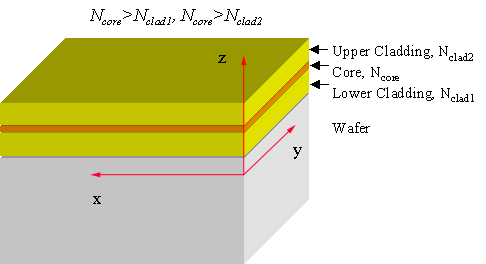
As it is well known, light can be confined in waveguides by a refractive index gradient. Light propagates in a core layer, surrounded with a cladding layer(s), which should be selected the core refractive index Ncore is greater than that of cladding Nclad: Ncore> Nclad. Cylindrical waveguides (optical fibers)
Optical fiber
An optical fiber is a flexible, transparent fiber made of a pure glass not much wider than a human hair. It functions as a waveguide, or "light pipe", to transmit light between the two ends of the fiber. The field of applied science and engineering concerned with the design and application of...
allow for one-dimensional light propagation along the axis. Planar waveguides, fabricated by sequential depositing flat layers of transparent materials with a proper refractive index gradient on a standard wafer, confine light in one direction (axis z) and permit free propagation in two others (axes x and y).
Light wave, propagating through the core, extends to some distinct into the both cladding layers. If the refractive index is modulated in the wave path, light of each given wavelength can be directed to a desirable point.
The DPH technology comprises design and fabrication of the holographic nano-structures inside a planar waveguide, providing light processing and control. There are many ways of modulating the core refractive index, the simplest of which is engraving the required pattern by nanolithography means. The modulation is created by embedding a digital hologram on the lower or upper core surface or on the both of them. According to NOD statement, standard lithographical processes can be used, making mass production straightforward and inexpensive. Nanoimprinting
Nanoimprint Lithography
Nanoimprint lithography is a method of fabricating nanometer scale patterns. It is a simple nanolithography process with low cost, high throughput and high resolution. It creates patterns by mechanical deformation of imprint resist and subsequent processes. The imprint resist is typically a monomer...
could be another viable method of fabricating DPH patterns.
Each DPH pattern is customized for a given application and computer-generated. It consists of numerous nano-grooves, each ~100 nm wide, positioned in a way, providing maximum efficiency for a specific application.
The devices are fabricated on standard wafers; one of typical devices is presented below (from the NOD web site). While the total number of nano-grooves is huge (≥106), a typical device size of DPH devices is on the millimeter scale.
Nano-Optic Devices, LLC (NOD) developed the DPH technology and applied it for fabricating Nano-Spectrometers and Optical Interconnects. There are additional numerous applications for the DPH in integrated optics.
The pictures below from the NOD web site demonstrate a DPH structure (left) and a nano-spectrometer hologram for the visible band (right).
