

DDR2 SDRAM
Encyclopedia

Double data rate
In computing, a computer bus operating with double data rate transfers data on both the rising and falling edges of the clock signal. This is also known as double pumped, dual-pumped, and double transition....
synchronous dynamic random-access memory interface. It supersedes the original DDR SDRAM
DDR SDRAM
Double data rate synchronous dynamic random access memory is a class of memory integrated circuits used in computers. DDR SDRAM has been superseded by DDR2 SDRAM and DDR3 SDRAM, neither of which are either forward or backward compatible with DDR SDRAM, meaning that DDR2 or DDR3 memory modules...
specification and has itself been superseded by DDR3 SDRAM
DDR3 SDRAM
In computing, DDR3 SDRAM, an abbreviation for double data rate type three synchronous dynamic random access memory, is a modern kind of dynamic random access memory with a high bandwidth interface. It is one of several variants of DRAM and associated interface techniques used since the early 1970s...
. DDR2 is neither forward
Forward compatibility
Forward compatibility or upward compatibility is a compatibility concept for systems design, as e.g. backward compatibility. Forward compatibility aims at the ability of a design to gracefully accept input intended for later versions of itself...
nor backward compatible
Backward compatibility
In the context of telecommunications and computing, a device or technology is said to be backward or downward compatible if it can work with input generated by an older device...
with either DDR or DDR3.
In addition to double pumping
Double data rate
In computing, a computer bus operating with double data rate transfers data on both the rising and falling edges of the clock signal. This is also known as double pumped, dual-pumped, and double transition....
the data bus as in DDR SDRAM (transferring data on the rising and falling edges of the bus clock signal), DDR2 allows higher bus speed and requires lower power by running the internal clock at half the speed of the data bus. The two factors combine to require a total of four data transfers per internal clock cycle. With data being transferred 64 bit
Bit
A bit is the basic unit of information in computing and telecommunications; it is the amount of information stored by a digital device or other physical system that exists in one of two possible distinct states...
s at a time, DDR2 SDRAM gives a transfer rate of (memory clock rate) × 2 (for bus clock multiplier) × 2 (for dual rate) × 64 (number of bits transferred) / 8 (number of bits/byte). Thus with a memory clock frequency of 100 MHz, DDR2 SDRAM gives a maximum transfer rate of 3200 MB
Megabyte
The megabyte is a multiple of the unit byte for digital information storage or transmission with two different values depending on context: bytes generally for computer memory; and one million bytes generally for computer storage. The IEEE Standards Board has decided that "Mega will mean 1 000...
/s
Second
The second is a unit of measurement of time, and is the International System of Units base unit of time. It may be measured using a clock....
.
Since the DDR2 internal clock runs at half the DDR external clock rate, DDR2 memory operating at the same external data bus clock rate as DDR results in DDR2 being able to provide the same bandwidth but with higher latency
SDRAM latency
SDRAM latency refers to delays in transmitting data between the CPU and SDRAM. SDRAM latency is often measured in memory bus clock cycles. However, the CPU operates faster than the memory, so it must wait while the proper segment of memory is located and read, before the data can be sent back...
. Consequently, DDR2 RAM possesses inferior performance. Alternatively, DDR2 memory operating at twice the external data bus clock rate as DDR may provide twice the bandwidth with the same latency. The best-rated DDR2 memory modules are at least twice as fast as the best-rated DDR memory modules.
Overview
Like all SDRAM implementations, DDR2 stores memory in memory cells that are activated with the use of a clock signalClock signal
In electronics and especially synchronous digital circuits, a clock signal is a particular type of signal that oscillates between a high and a low state and is utilized like a metronome to coordinate actions of circuits...
to synchronize their operation with an external data bus. Like DDR before it, the DDR2 I/O buffer transfers data both on the rising and falling edges of the clock signal (a technique called "double pumping"
Double data rate
In computing, a computer bus operating with double data rate transfers data on both the rising and falling edges of the clock signal. This is also known as double pumped, dual-pumped, and double transition....
). The key difference between DDR and DDR2 is that for DDR2 the memory cells are clocked at 1 quarter (rather than half) the rate of the bus
Computer bus
In computer architecture, a bus is a subsystem that transfers data between components inside a computer, or between computers.Early computer buses were literally parallel electrical wires with multiple connections, but the term is now used for any physical arrangement that provides the same...
. This requires a 4-bit-deep prefetch queue, but, without changing the memory cells themselves, DDR2 can effectively operate at twice the bus speed of DDR.
DDR2's bus frequency is boosted by electrical interface improvements, on-die termination
On-die termination
On-die termination is the technology where the termination resistor for impedance matching in transmission lines is located inside a semiconductor chip instead of on a printed circuit board.- Overview of electronic signal termination :...
, prefetch buffer
Prefetch buffer
A prefetch buffer is a data buffer employed on modern DRAM chips that allows quick and easy access to multiple data words located on a common physical row in the memory....
s and off-chip drivers. However, latency is greatly increased as a trade-off. The DDR2 prefetch buffer is 4 bits deep, whereas it is two bits deep for DDR and eight bits deep for DDR3
DDR3 SDRAM
In computing, DDR3 SDRAM, an abbreviation for double data rate type three synchronous dynamic random access memory, is a modern kind of dynamic random access memory with a high bandwidth interface. It is one of several variants of DRAM and associated interface techniques used since the early 1970s...
. While DDR SDRAM has typical read latencies of between 2 and 3 bus cycles, DDR2 may have read latencies between 4 and 6 cycles. Thus, DDR2 memory must be operated at twice the data rate to achieve the same latency.
Another cost of the increased bandwidth is the requirement that the chips are packaged in a more expensive and more difficult to assemble BGA
Ball grid array
A ball grid array is a type of surface-mount packaging used for integrated circuits.- Description :The BGA is descended from the pin grid array , which is a package with one face covered with pins in a grid pattern. These pins conduct electrical signals from the integrated circuit to the printed...
package as compared to the TSSOP
TSSOP
A TSSOP is a rectangular, thin body size surface mount component. A Type I TSSOP has legs protruding from the width portion of the package. A Type II TSSOP has the legs protruding from the length portion of the package...
package of the previous memory generations such as DDR SDRAM
DDR SDRAM
Double data rate synchronous dynamic random access memory is a class of memory integrated circuits used in computers. DDR SDRAM has been superseded by DDR2 SDRAM and DDR3 SDRAM, neither of which are either forward or backward compatible with DDR SDRAM, meaning that DDR2 or DDR3 memory modules...
and SDR SDRAM. This packaging change was necessary to maintain signal integrity at higher bus speeds.
Power savings are achieved primarily due to an improved manufacturing process through die shrinkage, resulting in a drop in operating voltage (1.8 V compared to DDR's 2.5 V). The lower memory clock frequency may also enable power reductions in applications that do not require the highest available data rates.
According to JEDEC the maximum recommended voltage is 1.9 volts and should be considered the absolute maximum when memory stability is an issue (such as in servers or other mission critical devices). In addition, JEDEC states that memory modules must withstand up to 2.3 volts before incurring permanent damage (although they may not actually function correctly at that level).
Chips and modules
For use in computers, DDR2 SDRAM is supplied in DIMMDIMM
A DIMM or dual in-line memory module, comprises a series of dynamic random-access memory integrated circuits. These modules are mounted on a printed circuit board and designed for use in personal computers, workstations and servers...
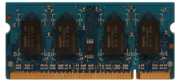
s with 240 pins and a single locating notch. Laptop DDR2 SO-DIMM
SO-DIMM
A SO-DIMM, or small outline dual in-line memory module, is a type of computer memory built using integrated circuits.SO-DIMMs are a smaller alternative to a DIMM, being roughly half the size of regular DIMMs...
s have 200 pins and often come identified by an additional S in their designation. DIMMs are identified by their peak transfer capacity (often called bandwidth).
| Standard name |
Memory clock (MHz) |
Cycle time (ns) |
I/O bus clock (MHz) |
Data rate (MT/s) |
Module name |
Peak transfer rate (MB/s) |
Timings Memory timings Memory timings refer collectively to a set of four numerical parameters called CL, tRCD, tRP, and tRAS, commonly represented as a series of four numbers separated with dashes, in that respective order . However, it is not unusual for tRAS to be omitted, or for a fifth value, the Command rate, to... (CL-tRCD-tRP) |
CAS latency CAS Latency Column Address Strobe latency, or CL, is the delay time between the moment a memory controller tells the memory module to access a particular memory column on a RAM memory module, and the moment the data from given array location is available on the module's output pins... (ns) |
|---|---|---|---|---|---|---|---|---|
| DDR2-400B DDR2-400C |
100 | 10 | 200 | 400 | PC2-3200 | 3200 | 3-3-3 4-4-4 |
15 20 |
| DDR2-533B DDR2-533C |
133⅓ | 7½ | 266⅔ | 533⅓ | PC2-4200* | 4266⅔ | 3-3-3 4-4-4 |
11¼ 15 |
| DDR2-667C DDR2-667D |
166⅔ | 6 | 333⅓ | 666⅔ | PC2-5300* | 5333⅓ | 4-4-4 5-5-5 |
12 15 |
| DDR2-800C DDR2-800D DDR2-800E |
200 | 5 | 400 | 800 | PC2-6400 | 6400 | 4-4-4 5-5-5 6-6-6 |
10 12½ 15 |
| DDR2-1066E DDR2-1066F |
266⅔ | 3¾ | 533⅓ | 1066⅔ | PC2-8500* | 8533⅓ | 6-6-6 7-7-7 |
11¼ 13⅛ |
Note: DDR2-xxx denotes data transfer rate, and describes raw DDR chips, whereas PC2-xxxx denotes theoretical bandwidth (with the last two digits truncated), and is used to describe assembled DIMMs. Bandwidth is calculated by taking transfers per second and multiplying by eight. This is because DDR2 memory modules transfer data on a bus that is 64 data bits wide, and since a byte comprises 8 bits, this equates to 8 bytes of data per transfer.
In addition to bandwidth and capacity variants, modules can
- Optionally implement ECC, which is an extra data byte lane used for correcting minor errors and detecting major errors for better reliability. Modules with ECC are identified by an additional ECC in their designation. PC2-4200 ECC is a PC2-4200 module with ECC.
- Be "registered", which improves signal integrity (and hence potentially clock rates and physical slot capacity) by electrically buffering the signals at a cost of an extra clock of increased latency. Those modules are identified by an additional R in their designation, whereas non-registered (a.k.a. "unbufferedUnbuffered memoryUnbuffered memory is RAM where there is no hardware register between the memory controller and the RAM chips. Unbuffered memory is the opposite of registered memory. Registered memory is more stable, one clock cycle slower, and more expensive than unbuffered memory...
") RAM may be identified by an additional U in the designation. PC2-4200R is a registered PC2-4200 module, PC2-4200R ECC is the same module but with additional ECC. - Be fully bufferedFully Buffered DIMMFully Buffered DIMM is a memory technology which can be used to increase reliability and density of memory systems. Conventionally, data lines from the memory controller have to be connected to data lines in every DRAM module. As memory width, as well as access speed, increases, the signal...
modules, which are designated by F or FB and do not have the same notch position as other classes. Fully buffered modules cannot be used with motherboards that are made for registered modules, and the different notch position physically prevents their insertion.
Note: registered and un-buffered SDRAM generally cannot be mixed on the same channel.
Note that the highest-rated DDR2 modules in 2009 operate at 533 MHz (1066 MT/s), compared to the highest-rated DDR modules operating at 200 MHz (400 MT/s). At the same time, the CAS latency of 11.2 ns = 6 / (Bus clock rate) for the best PC2-8500 modules is comparable to that of 10 ns = 4 / (Bus clock rate) for the best PC-3200 modules.
Debut
DDR2 was introduced in the second quarter of 2003 at two initial clock rates: 200 MHz (referred to as PC2-3200) and 266 MHz (PC2-4200). Both performed worse than the original DDR specification due to higher latency, which made total access times longer. However, the original DDR technology tops out at a clock rate around 200 MHz (400 MT/s). Higher performance DDR chips exist, but JEDECJEDEC
The JEDEC Solid State Technology Association, formerly known as the Joint Electron Devices Engineering Council , is an independent semiconductor engineering trade organization and standardization body...
has stated that they will not be standardized. These modules are mostly manufacturer optimizations of highest-yielding chips, drawing significantly more power than slower-clocked modules, and usually do not offer much, if any, greater real-world performance.
DDR2 started to become competitive with the older DDR standard by the end of 2004, as modules with lower latencies became available.
Backward compatibility
DDR2 DIMMs are not designed to be backward compatible with DDR DIMMs. The notch on DDR2 DIMMs is in a different position from DDR DIMMs, and the pin density is higher than DDR DIMMs in desktops. DDR2 is a 240-pin module, DDR is a 184-pin module. Notebooks have 200-pin modules for DDR and DDR2, however the notch on DDR modules is in a slightly different position than that on DDR2 modules.Higher performance DDR2 DIMMs are compatible with lower performance DDR2 DIMMs; however, the higher performance module runs at the lower module's frequency. Using lower performing DDR2 memory in a system capable of higher performance results in the bus running at the rate of the lowest performance memory in use; however, in many systems this performance hit can be mitigated to some extent by setting the timings of the memory to a lower latency setting.
See also
- DDR SDRAMDDR SDRAMDouble data rate synchronous dynamic random access memory is a class of memory integrated circuits used in computers. DDR SDRAM has been superseded by DDR2 SDRAM and DDR3 SDRAM, neither of which are either forward or backward compatible with DDR SDRAM, meaning that DDR2 or DDR3 memory modules...
- CAS latencyCAS LatencyColumn Address Strobe latency, or CL, is the delay time between the moment a memory controller tells the memory module to access a particular memory column on a RAM memory module, and the moment the data from given array location is available on the module's output pins...
(definition of "CAS 5-5-5-15", for example) - Dual-channel architectureDual-channel architectureMulti-channel architecture is a technology that increases the transfer speed of data between the RAM and the memory controller by adding more channels of communication between them. Theoretically this multiplies the data rate by exactly the number of channels present. Dual-channel memory employs...
- Fully Buffered DIMMFully Buffered DIMMFully Buffered DIMM is a memory technology which can be used to increase reliability and density of memory systems. Conventionally, data lines from the memory controller have to be connected to data lines in every DRAM module. As memory width, as well as access speed, increases, the signal...
- SO-DIMMSO-DIMMA SO-DIMM, or small outline dual in-line memory module, is a type of computer memory built using integrated circuits.SO-DIMMs are a smaller alternative to a DIMM, being roughly half the size of regular DIMMs...
- Unbuffered memoryUnbuffered memoryUnbuffered memory is RAM where there is no hardware register between the memory controller and the RAM chips. Unbuffered memory is the opposite of registered memory. Registered memory is more stable, one clock cycle slower, and more expensive than unbuffered memory...
- List of device bandwidths
- DDR3 SDRAMDDR3 SDRAMIn computing, DDR3 SDRAM, an abbreviation for double data rate type three synchronous dynamic random access memory, is a modern kind of dynamic random access memory with a high bandwidth interface. It is one of several variants of DRAM and associated interface techniques used since the early 1970s...
Further reading
- JEDEC standard: DDR2 SDRAM Specification (JESD79-2F, November 2009)
- JEDEC standard: DDR2-1066