
Crossover distortion
Encyclopedia
Crossover distortion is a type of distortion
which is caused by switching between devices driving a load, most often when the devices (such as a transistor
) are matched. It is most commonly seen in complementary, or "push-pull", Class-B amplifier stages, although it is occasionally seen in other types of circuits as well.
 The term crossover signifies the "crossing over" of the signal between devices, in this case, from the upper transistor to the lower and vice-versa. The term is not related to the audio crossover
—a filtering circuit which divides an audio signal into frequency bands.
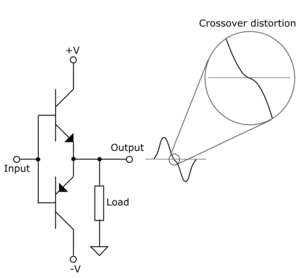 The image shows a typical class-B emitter-follower
complementary output stage. Under no signal conditions, the output is exactly mid-way between the supplies (i.e., at 0 V). When this is the case, the base-emitter bias of both the transistor
s is zero, so they are in the cut-off region where the transistors are not conducting.
Consider a positive going swing: As long as the input is less than the required forward VBE drop (≈ 0.65 V) of the upper NPN transistor, it will remain off or conduct very little - this is the same as a diode
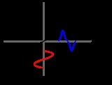
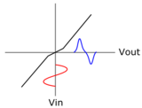
operation as far as the base circuit is concerned, and the output voltage does not follow the input (the lower PNP transistor is still off because its base-emitter diode is being reverse biased by the positive going input). The same applies for the lower transistor but for a negative going input. Thus, between about ±0.65 V of input, the output voltage is not a true replica or amplified version of the input, and we can see that as a "kink" in the output waveform near 0 V (or where one transistor stops conducting and the other starts). This kink is the most pronounced form of crossover distortion, and it becomes more evident and intrusive when the output voltage swing is reduced.
Less pronounced forms of distortion may be observed in this circuit as well. An emitter-follower will have a voltage gain of just under 1. In the circuit shown, the NPN emitter-follower and the PNP emitter-follower will generally have very slightly different voltage gains, leading to slightly different gains above and below ground. Other more subtle forms of crossover distortion, stemming from slight differences between the PNP and NPN devices, exist as well.
As with most kinds of distortion, another way in which crossover distortion can be reduced is through the use of feedback
. By comparing the output to the desired output, and adjusting the input to correct for any error, we can significantly reduce distortion. This may be done with an operational amplifier, as shown below, or with a discrete circuit.
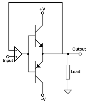 In the example shown, the operational amplifier is used to reduce the distortion of a push-pull pair. Op-amps are differential voltage amplifiers with very high gain (sometimes modeled as infinite gain). In an ideal model, the output of the op amp is held such that both inputs of the op amp must be at exactly the same voltage. In this case, since the inverting input is directly connected to the output, the voltage at the non-inverting input is always equal to the voltage at the output and inverting input, hence eliminating distortion. With a more precise model of an operational amplifier (with non-infinite gain) distortion is reduced by a factor equal to the gain of the op amp.
Most modern power amplifiers (including those used in hi-fi) employ both techniques, using both class-AB in their output stages, and feedback, offering reasonable efficiency and good distortion figures.
Distortion
A distortion is the alteration of the original shape of an object, image, sound, waveform or other form of information or representation. Distortion is usually unwanted, and often many methods are employed to minimize it in practice...
which is caused by switching between devices driving a load, most often when the devices (such as a transistor
Transistor
A transistor is a semiconductor device used to amplify and switch electronic signals and power. It is composed of a semiconductor material with at least three terminals for connection to an external circuit. A voltage or current applied to one pair of the transistor's terminals changes the current...
) are matched. It is most commonly seen in complementary, or "push-pull", Class-B amplifier stages, although it is occasionally seen in other types of circuits as well.
Audio crossover
Audio crossovers are a class of electronic filter used in audio applications. Most individual loudspeaker drivers are incapable of covering the entire audio spectrum from low frequencies to high frequencies with acceptable relative volume and lack of distortion so most hi-fi speaker systems use a...
—a filtering circuit which divides an audio signal into frequency bands.
Distortion mechanism
Common collector
In electronics, a common-collector amplifier is one of three basic single-stage bipolar junction transistor amplifier topologies, typically used as a voltage buffer...
complementary output stage. Under no signal conditions, the output is exactly mid-way between the supplies (i.e., at 0 V). When this is the case, the base-emitter bias of both the transistor
Transistor
A transistor is a semiconductor device used to amplify and switch electronic signals and power. It is composed of a semiconductor material with at least three terminals for connection to an external circuit. A voltage or current applied to one pair of the transistor's terminals changes the current...
s is zero, so they are in the cut-off region where the transistors are not conducting.
Consider a positive going swing: As long as the input is less than the required forward VBE drop (≈ 0.65 V) of the upper NPN transistor, it will remain off or conduct very little - this is the same as a diode
Diode
In electronics, a diode is a type of two-terminal electronic component with a nonlinear current–voltage characteristic. A semiconductor diode, the most common type today, is a crystalline piece of semiconductor material connected to two electrical terminals...
operation as far as the base circuit is concerned, and the output voltage does not follow the input (the lower PNP transistor is still off because its base-emitter diode is being reverse biased by the positive going input). The same applies for the lower transistor but for a negative going input. Thus, between about ±0.65 V of input, the output voltage is not a true replica or amplified version of the input, and we can see that as a "kink" in the output waveform near 0 V (or where one transistor stops conducting and the other starts). This kink is the most pronounced form of crossover distortion, and it becomes more evident and intrusive when the output voltage swing is reduced.
Less pronounced forms of distortion may be observed in this circuit as well. An emitter-follower will have a voltage gain of just under 1. In the circuit shown, the NPN emitter-follower and the PNP emitter-follower will generally have very slightly different voltage gains, leading to slightly different gains above and below ground. Other more subtle forms of crossover distortion, stemming from slight differences between the PNP and NPN devices, exist as well.
Possible solutions
In the case of a class B/AB amplifier, crossover distortion can be reduced by using a slight forward bias in the base circuit such that the transistors are idling at a small output current. The forward bias causes the circuit to operate in class-AB mode, so both transistors are slightly on during crossover. This can reduce or eliminate the characteristic kink of crossover distortion, although other types of crossover distortion will remain.As with most kinds of distortion, another way in which crossover distortion can be reduced is through the use of feedback
Feedback
Feedback describes the situation when output from an event or phenomenon in the past will influence an occurrence or occurrences of the same Feedback describes the situation when output from (or information about the result of) an event or phenomenon in the past will influence an occurrence or...
. By comparing the output to the desired output, and adjusting the input to correct for any error, we can significantly reduce distortion. This may be done with an operational amplifier, as shown below, or with a discrete circuit.
Most modern power amplifiers (including those used in hi-fi) employ both techniques, using both class-AB in their output stages, and feedback, offering reasonable efficiency and good distortion figures.