
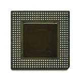
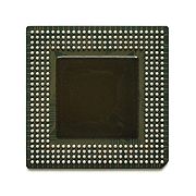
Ball grid array
Encyclopedia
Integrated circuit
An integrated circuit or monolithic integrated circuit is an electronic circuit manufactured by the patterned diffusion of trace elements into the surface of a thin substrate of semiconductor material...
s.
Description
Pin grid array
A pin grid array, often abbreviated PGA, is a type of integrated circuit packaging. In a PGA, the package is square or roughly square, and the pins are arranged in a regular array on the underside of the package...
(PGA), which is a package with one face covered (or partly covered) with pins in a grid pattern. These pins conduct electrical signals from the integrated circuit to the printed circuit board
Printed circuit board
A printed circuit board, or PCB, is used to mechanically support and electrically connect electronic components using conductive pathways, tracks or signal traces etched from copper sheets laminated onto a non-conductive substrate. It is also referred to as printed wiring board or etched wiring...
(PCB) on which it is placed. In a BGA, the pins are replaced by balls of solder
Solder
Solder is a fusible metal alloy used to join together metal workpieces and having a melting point below that of the workpiece.Soft solder is what is most often thought of when solder or soldering are mentioned and it typically has a melting range of . It is commonly used in electronics and...
stuck to the bottom of the package. These solder spheres can be placed manually or with automated equipment. The solder spheres are held in place with a tacky flux until soldering occurs. The device is placed
SMT Placement Equipment
SMT component placement systems, commonly called pick-and-place machines or P&Ps, are robotic machines which are used to place surface-mount devices onto a printed circuit board...
on a PCB with copper pads in a pattern that matches the solder balls. The assembly is then heated, either in a reflow oven
Reflow oven
A reflow oven is a machine used primarily for reflow soldering of surface mount electronic components to printed circuit boards .- Infrared and convection ovens :...
or by an infrared heater
Infrared heater
An infrared heater is a body with a higher temperature which transfers energy to a body with a lower temperature through electromagnetic radiation. Depending on the temperature of the emitting body, the wavelength of the infrared radiation ranges from 780 nm to 1 mm. The relationship...
, causing the solder balls to melt. Surface tension
Surface tension
Surface tension is a property of the surface of a liquid that allows it to resist an external force. It is revealed, for example, in floating of some objects on the surface of water, even though they are denser than water, and in the ability of some insects to run on the water surface...
causes the molten solder to hold the package in alignment with the circuit board, at the correct separation distance, while the solder cools and solidifies.
High density
The BGA is a solution to the problem of producing a miniature package for an integrated circuit with many hundreds of pins. Pin grid arrays and dual-in-line surface mount (SOICSmall-Outline Integrated Circuit
A small-outline integrated circuit is a surface-mounted integrated circuit package which occupies an area about 30–50% less than an equivalent DIP, with a typical thickness that is 70% less. They are generally available in the same pinouts as their counterpart DIP ICs...
) packages were being produced with more and more pins, and with decreasing spacing between the pins, but this was causing difficulties for the soldering process. As package pins got closer together, the danger of accidentally bridging adjacent pins with solder grew. BGAs do not have this problem when the solder is factory-applied to the package.
Heat conduction
A further advantage of BGA packages over packages with discrete leads (i.e. packages with legs) is the lower thermal resistance between the package and the PCB. This allows heat generated by the integrated circuit inside the package to flow more easily to the PCB, preventing the chip from overheating.Low-inductance leads
The shorter an electrical conductor, the lower its inductanceInductance
In electromagnetism and electronics, inductance is the ability of an inductor to store energy in a magnetic field. Inductors generate an opposing voltage proportional to the rate of change in current in a circuit...
, a property which causes unwanted distortion of signals in high-speed electronic circuits. BGAs, with their very short distance between the package and the PCB, have low inductances and therefore have far superior electrical performance to leaded devices.
Disadvantages
Noncompliant leads
A disadvantage of BGAs, however, is that the solder balls cannot flex in the way that longer leads can, they are not compliant. As with all surface mount devices, bending, due to a difference in coefficient of thermal expansionThermal expansion
Thermal expansion is the tendency of matter to change in volume in response to a change in temperature.When a substance is heated, its particles begin moving more and thus usually maintain a greater average separation. Materials which contract with increasing temperature are rare; this effect is...
between PCB substrate and BGA (thermal stress), or flexing and vibration (mechanical stress) can cause the solder joints to fracture.
Thermal expansion issues can be overcome by matching the mechanical and thermal characteristics of the PCB to those of the package. Typically, plastic BGA devices more closely match the PCB thermal characteristics than ceramic devices.
Mechanical stress issues can be overcome by bonding the devices to the board through a process called "under filling", which injects an epoxy mixture under the device after it is soldered to the PCB, effectively gluing the BGA device to the PCB. There are several types of under fill materials in use with differing properties relative to workability and thermal transfer. An additional advantage of under fill is that it limits tin whisker
Whisker (metallurgy)
Metal whiskering is a crystalline metallurgical phenomenon involving the spontaneous growth of tiny, filiform hairs from a metallic surface. The effect is primarily seen on elemental metals but also occurs with alloys....
growth.
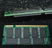
Another solution to non-compliant leads is to put a "compliant layer" in the package that allows the balls to physically move in relation to the package. This technique has become standard for packaging DRAMs in BGA packages.
Difficulty of inspection
Once the package is soldered down, it may be difficult to look for soldering faults. X-rayX-ray
X-radiation is a form of electromagnetic radiation. X-rays have a wavelength in the range of 0.01 to 10 nanometers, corresponding to frequencies in the range 30 petahertz to 30 exahertz and energies in the range 120 eV to 120 keV. They are shorter in wavelength than UV rays and longer than gamma...
machines, Industrial CT Scanning
Industrial CT Scanning
Industrial CT scanning is a process which uses X-ray equipment to produce three-dimensional representations of components both externally and internally. Industrial CT scanning has been used in many areas of industry for internal inspection of components...
machines
, and special microscopes have been developed to overcome this problem. If a BGA is found to be badly soldered, it can be removed in a rework station, which is a jig fitted with infrared lamp (or hot air), a thermocouple
Thermocouple
A thermocouple is a device consisting of two different conductors that produce a voltage proportional to a temperature difference between either end of the pair of conductors. Thermocouples are a widely used type of temperature sensor for measurement and control and can also be used to convert a...
and a vacuum device for lifting the package. The BGA can be replaced with a new one, or the BGA can be refurbished (or reballed) and re-installed on the circuit board. Packets of tiny ready-made solder balls are sold for reballing BGA's.
Due to cost of X-ray
X-ray
X-radiation is a form of electromagnetic radiation. X-rays have a wavelength in the range of 0.01 to 10 nanometers, corresponding to frequencies in the range 30 petahertz to 30 exahertz and energies in the range 120 eV to 120 keV. They are shorter in wavelength than UV rays and longer than gamma...
BGA inspection, electrical testing is very often used. Very common is boundary scan
Boundary scan
Boundary scan is a method for testing interconnects on printed circuit boards or sub-blocks inside an integrated circuit. Boundary scan is also widely used as a debugging method to watch integrated circuit pin states, measure voltage, or analyze sub-blocks inside an integrated circuit.The Joint...
testing using IEEE 1149.1 JTAG
JTAG
Joint Test Action Group is the common name for what was later standardized as the IEEE 1149.1 Standard Test Access Port and Boundary-Scan Architecture. It was initially devised for testing printed circuit boards using boundary scan and is still widely used for this application.Today JTAG is also...
port.
Difficulties with BGAs during circuit development
During development it is not practical to solder BGAs into place, and sockets are used instead, but tend to be unreliable. There are two common types of socket: the more reliable type has spring pins that push up under the balls, although it does not allow using BGAs with the balls removed as the spring pins may be too short.The less reliable type is a ZIF socket, with spring pinchers that grab the balls. This does not work well, especially if the balls are a bit small.
Cost of equipment
Expensive equipment is required to reliably solder BGA packages; hand-soldering BGA packages is very difficult and unreliable, usable only for the smallest packages in the smallest quantities.Variants
- CBGA and PBGA denote the Ceramic or Plastic substrate material to which the array is attached.
- CABGA: Chip Array Ball Grid Array
- CTBGA: Thin Chip Array Ball Grid Array
- CVBGA: Very Thin Chip Array Ball Grid Array
- DSBGA: Die-Size Ball Grid Array
- FBGA or Fine Ball Grid Array based on ball grid array technology. It has thinner contacts and is mainly used in system-on-a-chipSystem-on-a-chipA system on a chip or system on chip is an integrated circuit that integrates all components of a computer or other electronic system into a single chip. It may contain digital, analog, mixed-signal, and often radio-frequency functions—all on a single chip substrate...
designs.- Known as FineLine BGA by Altera.
- FCmBGA: Flip Chip Molded Ball Grid Array
- LFBGA: Low-profile Fine-pitch Ball Grid Array
- UFBGA and UBGA and Ultra Fine Ball Grid Array based on pitch ball grid array.
- MBGA: Micro Ball Grid Array
- PBGA: Plastic Ball Grid Array
- MCM-PBGA: Multi-Chip Module Plastic Ball Grid Array
- TEPBGA: Thermally Enhanced Plastic Ball Grid Array
- SuperBGA (SBGA): Super Ball Grid Array
- TABGA / TBGA: Tape Array BGA
- TFBGA or Thin and Fine Ball Grid Array
See also
- Dual in-line packageDual in-line packageIn microelectronics, a dual in-line package is an electronic device package with a rectangular housing and two parallel rows of electrical connecting pins. The package may be through-hole mounted to a printed circuit board or inserted in a socket.A DIP is usually referred to as a DIPn, where n is...
(DIP) - Pin grid arrayPin grid arrayA pin grid array, often abbreviated PGA, is a type of integrated circuit packaging. In a PGA, the package is square or roughly square, and the pins are arranged in a regular array on the underside of the package...
(PGA) - Land grid arrayLand grid arrayThe land grid array is a type of surface-mount packaging for integrated circuits that is notable for having the pins on the socket rather than the integrated circuit...
(LGA) - TQFPTQFPA thin quad flat pack is a type of surface-mounted package. TQFPs provide the same benefits of the metric QFP, but are thinner and have a standard lead-frame footprint ....
(thin quad flat pack) - Small-outline integrated circuitSmall-Outline Integrated CircuitA small-outline integrated circuit is a surface-mounted integrated circuit package which occupies an area about 30–50% less than an equivalent DIP, with a typical thickness that is 70% less. They are generally available in the same pinouts as their counterpart DIP ICs...
(SOIC) - Chip carrierChip carrierA chip carrier, also known as a chip container or chip package, is a container for a transistor or an integrated circuit. The carrier usually provides metal leads, or "pins", which are sturdy enough to electrically and mechanically connect the fragile chip to a circuit board. This connection may be...
Chip packaging and package types list