
2DEG
Encyclopedia
A two-dimensional electron gas (2DEG) is a gas of electron
s free to move in two dimensions, but tightly confined in the third. This tight confinement leads to quantized energy level
s for motion in that direction, which can then be ignored for most problems. Thus the electrons appear to be a 2D sheet embedded in a 3D world. The analogous construct of holes
is called a two-dimensional hole gas (2DHG), and such systems have many useful and interesting properties.

 Most 2DEGs are found in transistor
-like structures made from semiconductor
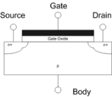
s. The most commonly encountered 2DEG is the layer of electrons found in MOSFET
s. When the transistor is in inversion mode, the electrons underneath the gate oxide
are confined to the semiconductor-oxide interface, and thus occupy well defined energy levels. Nearly always, only the lowest level is occupied, and so the motion of the electrons perpendicular to the interface can be ignored. However, the electron is free to move parallel to the interface, and so is quasi two-dimensional.
Other methods for engineering 2DEGs are high-electron-mobility-transistor
s (HEMTs) and rectangular quantum well
s. HEMT
s are field-effect transistors that utilize the heterojunction
between two semiconducting materials to confine electrons to a triangular quantum well
. Electrons confined to the heterojunction
of HEMTs exhibit higher mobilities
than those in MOSFETs, since the former device utilizes an intentionally undoped channel thereby mitigating the deleterious effect of ionized impurity scattering
. Two closely spaced heterojunction
interfaces may be used to confine electrons to a rectangular quantum well
. Careful choice of the materials and alloy compositions allow control of the carrier densities within the 2DEG.
Electrons may also be confined to the surface of a material. For example, free electrons will float on the surface of liquid helium
, and are free to move along the surface, but stick to the helium; some of the earliest work in 2DEGs was done using this system[1]. It is also possible to attract electrons onto the surface of graphene
sheets, using the field effect. This has been a topic of current research, due to the applications of carbon nanotubes to quantum computing and single electron transistors.
electrons, especially at low temperatures. When cooled to 4 K, 2DEGs may have mobilities of the order of 1,000,000 cm^2/Vs and lower temperatures can lead to further increase of
  . Specially grown, state of the art heterostructures with mobilities around 30,000,000 cm²/(V·s) have been made[4]. These enormous mobilities offer a test bed for exploring fundamental physics, since besides confinement and effective mass, the electrons do not interact with the semiconductor very often, sometimes traveling several micrometers
before colliding; this so called mean free path can be estimated in the parabolic band approximation as

where is the electron density in the 2DEG. Note that
  typically depends on
  .[6]
.[6]
Aside from being in practically every semiconductor device in use today, two dimensional systems allow access to interesting physics. The quantum Hall effect was first observed in a 2DEG[2], which led to two Nobel Prize
s, in 1985 and 1998. Spectrum of a laterally modulated 2DEG (a two-dimensional superlattice
) subject to magnetic field can be represented as the Hofstadter's butterfly
, a fractal structure in the energy vs plot, signatures of which were observed in transport experiments.[5]
Full control of the 2DEG spin polarization
was recently demonstrated by C. Phelps et al.[3], which could be useful in quantum information technology
...
Electron
The electron is a subatomic particle with a negative elementary electric charge. It has no known components or substructure; in other words, it is generally thought to be an elementary particle. An electron has a mass that is approximately 1/1836 that of the proton...
s free to move in two dimensions, but tightly confined in the third. This tight confinement leads to quantized energy level
Energy level
A quantum mechanical system or particle that is bound -- that is, confined spatially—can only take on certain discrete values of energy. This contrasts with classical particles, which can have any energy. These discrete values are called energy levels...
s for motion in that direction, which can then be ignored for most problems. Thus the electrons appear to be a 2D sheet embedded in a 3D world. The analogous construct of holes
Electron hole
An electron hole is the conceptual and mathematical opposite of an electron, useful in the study of physics, chemistry, and electrical engineering. The concept describes the lack of an electron at a position where one could exist in an atom or atomic lattice...
is called a two-dimensional hole gas (2DHG), and such systems have many useful and interesting properties.
Geometries
Transistor
A transistor is a semiconductor device used to amplify and switch electronic signals and power. It is composed of a semiconductor material with at least three terminals for connection to an external circuit. A voltage or current applied to one pair of the transistor's terminals changes the current...
-like structures made from semiconductor
Semiconductor
A semiconductor is a material with electrical conductivity due to electron flow intermediate in magnitude between that of a conductor and an insulator. This means a conductivity roughly in the range of 103 to 10−8 siemens per centimeter...
s. The most commonly encountered 2DEG is the layer of electrons found in MOSFET
MOSFET
The metal–oxide–semiconductor field-effect transistor is a transistor used for amplifying or switching electronic signals. The basic principle of this kind of transistor was first patented by Julius Edgar Lilienfeld in 1925...
s. When the transistor is in inversion mode, the electrons underneath the gate oxide
Gate oxide
The gate oxide is the dielectric layer that separates the gate terminal of a MOSFET from the underlying source and drain terminals as well as the conductive channel that connects source and drain when the transistor is turned on. Gate oxide is formed by oxidizing the silicon of the channel to form...
are confined to the semiconductor-oxide interface, and thus occupy well defined energy levels. Nearly always, only the lowest level is occupied, and so the motion of the electrons perpendicular to the interface can be ignored. However, the electron is free to move parallel to the interface, and so is quasi two-dimensional.
Other methods for engineering 2DEGs are high-electron-mobility-transistor
HEMT
High electron mobility transistor , also known as heterostructure FET or modulation-doped FET , is a field effect transistor incorporating a junction between two materials with different band gaps as the channel instead of a doped region, as is generally the case for MOSFET...
s (HEMTs) and rectangular quantum well
Quantum well
A quantum well is a potential well with only discrete energy values.One technology to create quantization is to confine particles, which were originally free to move in three dimensions, to two dimensions, forcing them to occupy a planar region...
s. HEMT
HEMT
High electron mobility transistor , also known as heterostructure FET or modulation-doped FET , is a field effect transistor incorporating a junction between two materials with different band gaps as the channel instead of a doped region, as is generally the case for MOSFET...
s are field-effect transistors that utilize the heterojunction
Heterojunction
A heterojunction is the interface that occurs between two layers or regions of dissimilar crystalline semiconductors. These semiconducting materials have unequal band gaps as opposed to a homojunction...
between two semiconducting materials to confine electrons to a triangular quantum well
Quantum well
A quantum well is a potential well with only discrete energy values.One technology to create quantization is to confine particles, which were originally free to move in three dimensions, to two dimensions, forcing them to occupy a planar region...
. Electrons confined to the heterojunction
Heterojunction
A heterojunction is the interface that occurs between two layers or regions of dissimilar crystalline semiconductors. These semiconducting materials have unequal band gaps as opposed to a homojunction...
of HEMTs exhibit higher mobilities
Electron mobility
In solid-state physics, the electron mobility characterizes how quickly an electron can move through a metal or semiconductor, when pulled by an electric field. In semiconductors, there is an analogous quantity for holes, called hole mobility...
than those in MOSFETs, since the former device utilizes an intentionally undoped channel thereby mitigating the deleterious effect of ionized impurity scattering
Ionized impurity scattering
Ionized impurity scattering is the scattering of charge carriers by ionization in the lattice. The most primitive models can be conceptually understood as a particle responding to unbalanced local charge that arises near a crystal impurity; not dissimilar to an electron encountering an electric field...
. Two closely spaced heterojunction
Heterojunction
A heterojunction is the interface that occurs between two layers or regions of dissimilar crystalline semiconductors. These semiconducting materials have unequal band gaps as opposed to a homojunction...
interfaces may be used to confine electrons to a rectangular quantum well
Quantum well
A quantum well is a potential well with only discrete energy values.One technology to create quantization is to confine particles, which were originally free to move in three dimensions, to two dimensions, forcing them to occupy a planar region...
. Careful choice of the materials and alloy compositions allow control of the carrier densities within the 2DEG.
Electrons may also be confined to the surface of a material. For example, free electrons will float on the surface of liquid helium
Liquid helium
Helium exists in liquid form only at extremely low temperatures. The boiling point and critical point depend on the isotope of the helium; see the table below for values. The density of liquid helium-4 at its boiling point and 1 atmosphere is approximately 0.125 g/mL Helium-4 was first liquefied...
, and are free to move along the surface, but stick to the helium; some of the earliest work in 2DEGs was done using this system[1]. It is also possible to attract electrons onto the surface of graphene
Graphene
Graphene is an allotrope of carbon, whose structure is one-atom-thick planar sheets of sp2-bonded carbon atoms that are densely packed in a honeycomb crystal lattice. The term graphene was coined as a combination of graphite and the suffix -ene by Hanns-Peter Boehm, who described single-layer...
sheets, using the field effect. This has been a topic of current research, due to the applications of carbon nanotubes to quantum computing and single electron transistors.
Experiments
Considerable research involving 2DEGs and 2DHGs has been done, and much continues to this day. 2DEGs offer a mature system of extremely high mobilityElectron mobility
In solid-state physics, the electron mobility characterizes how quickly an electron can move through a metal or semiconductor, when pulled by an electric field. In semiconductors, there is an analogous quantity for holes, called hole mobility...
electrons, especially at low temperatures. When cooled to 4 K, 2DEGs may have mobilities
of the order of 1,000,000 cm^2/Vs and lower temperatures can lead to further increase of . Specially grown, state of the art heterostructures with mobilities around 30,000,000 cm²/(V·s) have been made[4]. These enormous mobilities offer a test bed for exploring fundamental physics, since besides confinement and effective mass, the electrons do not interact with the semiconductor very often, sometimes traveling several micrometersMicrometre
A micrometer , is by definition 1×10⁻⁶ of a meter .In plain English, it means one-millionth of a meter . Its unit symbol in the International System of Units is μm...
before colliding; this so called mean free path
can be estimated in the parabolic band approximation aswhere
is the electron density in the 2DEG. Note that typically depends on .[6]Aside from being in practically every semiconductor device in use today, two dimensional systems allow access to interesting physics. The quantum Hall effect was first observed in a 2DEG[2], which led to two Nobel Prize
Nobel Prize
The Nobel Prizes are annual international awards bestowed by Scandinavian committees in recognition of cultural and scientific advances. The will of the Swedish chemist Alfred Nobel, the inventor of dynamite, established the prizes in 1895...
s, in 1985 and 1998. Spectrum of a laterally modulated 2DEG (a two-dimensional superlattice
Superlattice
Superlattice is a periodic structure of layers of two materials. Typically, the thickness of one layer is several nanometers.- Discovery :Superlattices were discovered early in the 20th century through their special X-ray diffraction patterns....
) subject to magnetic field
can be represented as the Hofstadter's butterflyHofstadter's butterfly
Hofstadter's butterfly is the name of a fractal structure discovered by Douglas Hofstadter, which he described in 1976 in an article on the energy levels of Bloch electrons in magnetic fields. It gives a graphical representation of the spectrum of the almost Mathieu operator for \lambda = 1 at...
, a fractal structure in the energy vs
plot, signatures of which were observed in transport experiments.[5]Full control of the 2DEG spin polarization
Spin polarization
Spin polarization is the degree to which the spin, i.e., the intrinsic angular momentum of elementary particles, is aligned with a given direction. This property may pertain to the spin, hence to the magnetic moment, of conduction electrons in ferromagnetic metals, such as iron, giving rise to...
was recently demonstrated by C. Phelps et al.[3], which could be useful in quantum information technology
Quantum information science
Quantum information science is an area of study based on the idea that information science depends on quantum effects in physics. It includes theoretical issues in computational models as well as more experimental topics in quantum physics including what can and cannot be done with quantum...
...
Footnotes
- 1. W. T. Sommer Liquid Helium as a Barrier to Electrons Physical Review Letters 12, 271-273 (1964)
- 2. K. v. Klitzing, G. Dorda, and M. Pepper New Method for High-Accuracy Determination of the Fine-Structure Constant Based on Quantized Hall Resistance, Physical Review Letters 45, 494-497 (1980).
- 3. C. Phelps, T. Sweeney, R. Cox, and H. Wang Ultrafast Coherent Electron Spin Flip in a CdTe Quantum Well, Physical Review Letters 102, 237402 (2009).
- 4. A. Kumar, G. A. Csáthy, M. J. Manfra, L. N. Pfeiffer, and K. W. West, Nonconventional Odd-Denominator Fractional Quantum Hall States in the Second Landau Level, Physical Review Letters 105, 246808 (2010); also arXiv:1009.0237.
- 5. M. C. Geisler, J. H. Smet, V. Umansky, K. von Klitzing, B. Naundorf, R. Ketzmerick, and H. Schweizer, Detection of a Landau Band-Coupling-Induced Rearrangement of the Hofstadter Butterfly, Physical Review Letters 92, 256801 (2004).
- 6. W. Pan, N. Masuhara, N. S. Sullivan, K. W. Baldwin, K. W. West, L. N. Pfeiffer, and D. C. Tsui, Impact of Disorder on the 5/2 Fractional Quantum Hall State, Physical Review Letters 106, 206806 (2011); also arXiv:1109.6911.